
 Open Access Article
 This Open Access Article is licensed under a Creative Commons Attribution-Non Commercial 3.0 Unported Licence
Hydrogen-driven dramatically improved mechanical properties of amorphized ITO–Ag–ITO thin films
Sungmin Park a,
Janghee Yoonb,
Seohan Kim*cd and
Pungkeun Song*a
a,
Janghee Yoonb,
Seohan Kim*cd and
Pungkeun Song*a
aDepartment of Materials Science and Engineering, Pusan National University, Busan 46241, Korea
bBusan Center, Korea Basic Science Institute, Busan 46742, Korea
cMaterials Technology Research Institute, Pusan National University, Busan 46241, Korea. E-mail: seohahnkim@pusan.ac.kr
dDepartment of Engineering Science, The Ångström Laboratory, Uppsala University, SE 75121, Sweden
First published on 15th January 2021
Abstract
An oxide/metal/oxide (OMO) multi-structure, which has good electrical, optical, and mechanical stability, was studied as a potential replacement of polycrystalline In–Sn–O (ITO). However, the degradation of mechanical properties caused by the polycrystalline structure of the top layer forming on the polycrystalline metal layer needs to be improved. To address this issue, we introduced hydrogen in the oxide layers to form a stabilized amorphous oxide structure despite it being deposited on the polycrystalline layer. An ITO/Ag/ITO (IAI) structure was used in this work, and we confirmed that the correct amount of hydrogen introduction can improve mechanical stability without any deterioration in optical and electrical properties. The hydrogen presence in the IAI as intended was confirmed, and the assumption was that the hydrogen suppressed the formation of microcracks on the ITO surface due to low residual stress that came from decreased subgap level defects. This assumption was clearly confirmed with the electrical properties before and after dynamic bending testing. The results imply that we can adjust not only IAI structures with high mechanical stability due to the right amount of hydrogen introduction to make stabilized amorphous oxide but also almost all oxide/metal/oxide structures that contain unintended polycrystalline structures.
Introduction
Electronic devices are continually becoming ever smaller, lighter, and more compact, and this is driven by consumer needs and the rapid development of technology. Transparent electrodes (TEs) are becoming increasingly important as front electrodes in electronic devices such as flexible displays, touchpads, flat panel displays, solar cells, organic light emitting devices (OLEDs), and smart windows.1–5 Generally, TEs can be classified into oxides and oxide-free materials. Oxide-free TEs include metal mesh, carbon-based TEs, silver nanowire (AgNW), and conductive polymer.6–9 Despite their high electrical conductivity, however, it is hard to apply them commercially due to optical problems such as haze and chemical instability.7,8 In contrast, TEs based on oxides, such as transparent conductive oxides (TCOs), have been studied because of their high electrical conductivity and optical transmittance in the visible light region.9 Nowadays, with the advancement of technological development, flexibility is one of the key properties of TCOs.10–12 TCOs employed in OLEDs, touch panels, and solar cells, for example, have been studied for their ability to obtain low sheet resistance and high transmittance, and much of this relates to crystallization.13–17 However, it is difficult to apply polycrystalline TCOs in flexible devices because of its low mechanical stability and grain boundary that can easily generate and propagate cracks.18,19 For such reasons, many research groups have aimed to improve crystallization temperature20–22 or stabilize oxide-free materials.23,24The use of TE in devices has been found to incur several problems. For example, AgNW has low transmittance due to the haze phenomenon, poor device efficiency, and poor adhesion to the substrate.25 Carbon nanotubes and conducting polymers are also difficult to adjust because carbon nanotubes make it hard to disperse uniformly,26 and the energy band gap of conducting polymers is less than 3 eV, meaning it is absorbed light in the visible wavelength range.27 Furthermore, even if these disadvantages are overcome, due to the high processing cost and difficulty of mass production, it is still difficult to replace TCOs. Therefore, our study proposed oxide/metal/oxide (OMO) structures from previous work.28–30 An OMO structure has high electrical, optical, and mechanical properties compared with crystalline TCOs;31 the high electrical properties are due to the metal layer, and the high mechanical properties owe to the ductility of metal.32 The high optical transmittance comes from the index-matched refractive ratio between the oxide and the metal layers.33 Furthermore, OMO structures can be produced at low cost because it can be used without post treatment such as post annealing or chemical treatment. There have been numerous studies on OMO thin films, including those that use indium tin oxide and indium zinc oxide, such as ITO/Ag/ITO, TiO2/Ag/TiO2, IZO/Ag/IZO and WO3/Ag/WO3.34–37 Among them, the most widely used OMO structure is ITO/Ag/ITO.28,34,38–41
Nevertheless, the mechanical stability of OMO structures presents ongoing problems. Generally, thin films deposited on a polycrystalline structure can easily crystallize,42 and it is well known that the metal layer between oxide layers easily crystallizes despite the thin thickness of around 10 nm.43 The bottom oxide layer has an amorphous structure when it forms on a glass substrate; however, the upper oxide layer deposited on polycrystalline metal has a crystalline structure.44 As a result, an OMO structure has a polycrystalline oxide/metal/amorphous oxide structure, and the top crystallized oxide layer is a weak point with low mechanical stability. In our previous work,45,46 we demonstrated the hydrogen passivation effect on In2O3-based TCO materials, and that hydrogen plays a crucial role in mechanical stability. The hydrogen in TCOs contributes to mechanical stability with a stabilized amorphous structure and suppression of subgap defects in oxide material, which can release residual stress in thin films.
In this work, we demonstrate that an ITO/Ag/ITO structure can improve its mechanical stability by using hydrogen-doped oxide layers on both the bottom and the top oxides layers without any complicated process. The ITO/Ag/ITO structure was prepared with various hydrogen flow ratios [H2/(H2 + Ar)] from 0% to 0.8% on a polyethylene terephthalate (PET) substrate. These results can be applied not only to all kinds of OMO structures that including unintended polycrystalline top oxide layers but also TCO thin films requiring mechanical stability.
Experimental
The ITO/Ag/ITO (IAI) multilayer is prepared on a PET substrate (50 × 50 × 0.25 mm3) for measuring mechanical stability, and a SiO/Si (50 × 3 × 0.25 mm3) for residual stress test. And the glass substrate (50 × 50 × 0.78 mm3) is used for electrical and optical properties. The oxide layers were deposited using a DC magnetron sputtering system with a single sintered ITO target (9.8 wt% SnO2 doped In2O3) without intensive substrate heating. The base pressure was exhausted to 1.0 × 10⁻⁶ Torr, and the working pressure of 7.5 mTorr was maintained during the deposition processes. The discharge power was 100 W and 50 W for ITO and Ag, respectively. The distance between the substrate and the target was 50 mm for ITO and 100 nm for silver. Firstly, the bottom ITO layer (40 nm) was deposited using a mixture of pure argon gas (6 N, 99.9999%) and hydrogen gas (6 N, 99.9999%); the gas flow ratio H2/(H2 + Ar) was varied from 0.0, 0.1, 0.2, 0.4, and 0.8%. Secondly, the Ag layer was deposited on an amorphous bottom ITO:H layer using pure argon gas. Then, the top ITO layer was deposited with the same method as the bottom ITO:H layer. The electrical and optical properties were measure by a Hall effect measurement system (ECOPIA, HMS-3000) and an UV-Vis spectrophotometer (UV-1800, SHIMADZU) in the range of 200–1100 nm, respectively. The thickness of thin film was confirmed by scanning electron microscopy (SEM, MIRA3, TESCAN) and spectral reflectometer (ST2000-DLXn, K-MAC). The mechanical property of IAI films deposited on PET (size: 10 × 40 × 0.25 mm3) was estimated by the resistance change under cycling bending with a digital multimeter (Agilent 34401A), 0.5 Hz bending frequency, and 5 mm bending radius. The thermal emissivity of the IAI structure were estimated using an infrared camera (IR camera, Nikon), and 3 V was applied to the IAI structure. The residual stress in the thin film was evaluated from the change in curvature of the thin film according to laser irradiation at regular intervals (5 mm) to investigate the residual stress in the thin film (residual stress test, J&L Tech Co.). In this case, the IAI structure was deposited on a silicon substrate with dimensions of 5 × 50 × 0.28 mm3. Time-of-flight secondary ion mass spectrometry (TOF-SIMS, ION-TOF GmbH, Münster) was performed with a pulsed 30 keV Bi+ primary beam with a current of 1.01 pA using Cs sputter gun of 2 keV and 15 nA. The analyzed area was 200 × 200 μm. Negative ion spectra were internally calibrated using H−, C−, C2−, C3−, and C4− peaks normalized to the respective secondary total ion yields. The structure of IAI multilayer was investigated by X-ray diffraction (XRD, D8 Advance, Bruker).Results and discussion
A hydrogen-doped ITO layer (ITO:H) was introduced with both a bottom and a top layer of ITO/Ag/ITO (IAI:H). Fig. 1 shows the TOF-SIMS depth profiling results of IAI:H thin films in relation to the hydrogen flow ratios. That hydrogen exists in the sample prepared without hydrogen flow was confirmed in our previous work.46 The monotonic increase of hydrogen concentration in the top and bottom oxide layers is confirmed, indicating that hydrogen was successfully introduced and present in the IAI:H structure as intended.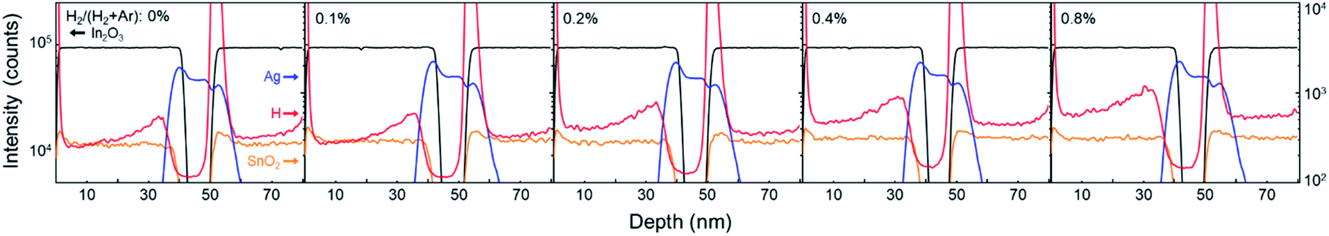 | ||
| Fig. 1 Depth profiling results in relation to H2/(H2 + Ar) flow ratio from 0 to 0.8% on bottom and top oxides layers. The hydrogen concentration in thin film increased with hydrogen flow ratios as intended. The black, blue, red, and orange indicates In2O3, Ag, H, and SnO2, respectively. | ||
Generally, the ITO with thickness of 40 nm deposited on glass without substrate heating has an amorphous structure,28,46 and the Ag layer is easily crystallized even thin thickness and low substrate temperature. And the ITO has poly-crystalline structure when deposited on poly-crystalline metal layer.28 Therefore, the IAI structure without hydrogen shows a preferential orientation of ITO C(222) and Ag C(111), as shown in Fig. 2. The XRD patterns of IAI:H with various hydrogen flow ratios is shown in Fig. 2. As mentioned already, IAI without hydrogen shows a highly preferred orientation C(222) of ITO; on the other hand, IAI:H shows a decrease in the intensity of C(222) with increasing hydrogen concentration. This indicates that the polycrystalline top ITO layer modulates the structure into an amorphous one with hydrogen introduction.
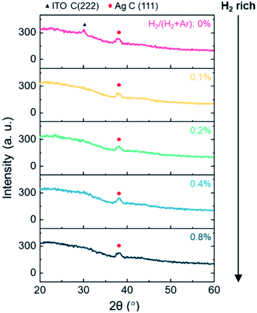 | ||
| Fig. 2 XRD patterns of ITO:H/Ag/ITO:H multi-structures as increasing H2/(H2 + Ar) ratio. The black triangle and red circle indicates ITO C(222) and Ag C(111), respectively. | ||
Fig. 3 shows (a) the schematic diagram of the dynamic bending test, and (b) resistance change of the IAI:H thin film in various H2/(H2 + Ar) ratios. The bending radius is 5 mm and 2 seconds for 1 cycle, as shown in Fig. 3(a). The resistance change during the dynamic bending stress is determined as ΔR/Rn, and ΔR means (=Rn+1 − Rn). This shows resistance change trends more clearly during the dynamic bending test. In the case of IAI without hydrogen, it shows unstable changes due to the low mechanical stability that comes from the top polycrystalline ITO, as shown in Fig. 2. The IAI:H with 0.2% hydrogen concentration shows the most stable and lowest trends in resistance. The resistance change trend decreases sharply until 0.2%, then slightly increases. However, compared with the no hydrogen IAI, it shows a stable change. This means that a hydrogen-doped top ITO layer has an amorphous structure, and it allows mechanical stability by interrupting the propagation of cracks compared with a polycrystalline structure.
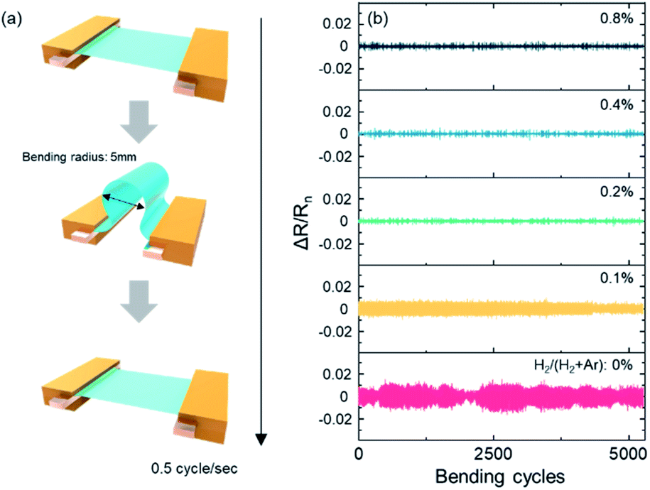 | ||
| Fig. 3 (a) The schematics of dynamic bending test; the bending radius is 5 mm, the time for 1 cycle is 2 s and 0.5 s interval for each measuring. (b) The resistance change ratio (ΔR/Rn) in relation to H2/(H2 + Ar) ratio and ΔR is determined as Rn+1 − Rn. | ||
Most sputtered thin films have a compressive stress inside of them due to the characteristics of the sputtering process that stem from the bombardment of incident particles during deposition.47 Residual stress becomes the cause of deterioration in electrical, optical, and mechanical properties.48 In order to determine the cause of deterioration of mechanical stability, the average value of the resistance change trend and residual stress of IAI thin films were measured and are displayed in Fig. 4. The details of the residual stress measuring system was discussed in our previous study.45 As shown in Fig. 4(a), the average value of resistance changes during the dynamic bending test (5000 cycles), decreases until the hydrogen flow of 0.2%, and then slightly increases with a higher hydrogen flow ratio. The residual stress in IAI:H shows good agreement with the average change in resistance; it shows the lowest value for the sample with the 0.2% hydrogen flow. It clearly shows that the proper amount of hydrogen on both the top and bottom ITO layers can improve mechanical stability due to the amorphized oxide layer, despite it being deposited on a polycrystalline metal layer.
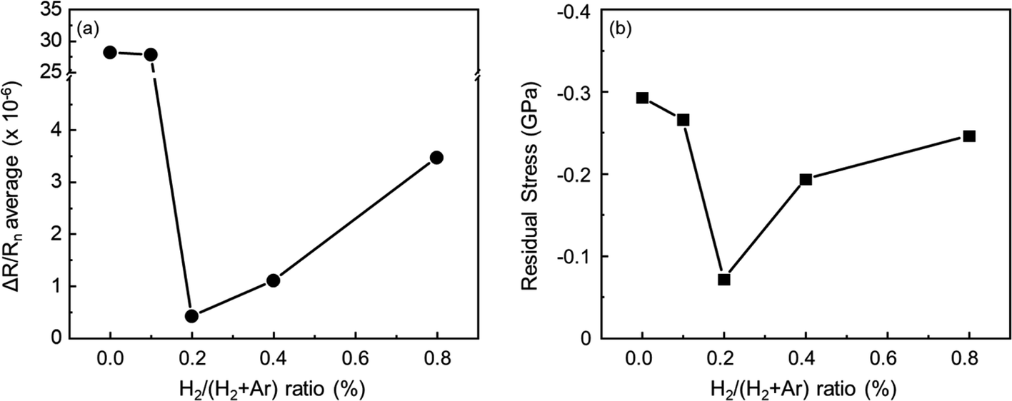 | ||
| Fig. 4 (a) The residual stress and (b) average ΔR/Rn of ITO:H/Ag/ITO:H multi structure in relation to H2/(H2 + Ar) ratio. It is clear that multi structure with hydrogen doped ITO on top and bottom layers has low internal stress. | ||
Fig. 5 depicts (a) the carrier concentration (n), mobility (μ), and resistivity (ρ) before (solid line with closed symbol) and after (dash line with open symbol) the 5000 cycles dynamic bending test as a function of hydrogen flow ratios. The electrical properties of the IAI:H before bending show similar values regardless of hydrogen flow, as discussed in previous work.46 In the case of after the bending test, the ρ and the μ dramatically decrease. Generally, in TCOs, the ρ is determined by the correlation between the n and the μ; The μ is dominated by the ionization scattering of the n, that is, the changes in the μ are interpreted by the n.49 However, in this case, the result can be assumed to be due to the microcracks forming on the film surface causing a decrease of μ. The smallest change in the μ of IAI:H with 0.2% hydrogen flow compared with the other sample is strong evidence for the assumption. As a result, the stabilized oxide layer with hydrogen can improve mechanical stability due to the suppression of microcracks on the film surface that can reduce μ. The absorption coefficient (α) and transmittance in the visible light region is shown in Fig. 5(b) and inset. The α is calculated from the equation α = −ln[T/(1 −R)]/d, where T and R are the transmittance and reflectance, and d is the film thickness. There is no significant difference in transmittance because all the samples have almost the same n; however, it shows a difference in α as a function of hydrogen flow ratio. The α without hydrogen yields a high value compared with IAI:H. It seems that the hydrogen in the oxide layers suppresses the subgap level defect that manipulates microcracks on film surfaces, as discussed in previous work.46
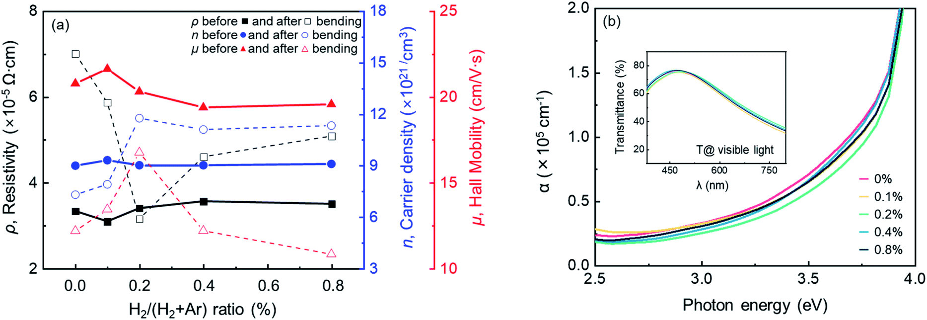 | ||
| Fig. 5 (a) The hall effect measurements results before (solid line with closed symbol) and after (dash line with open symbol) 5000 cycles dynamic bending test and (b) the absorption coefficient of IAI:H as increasing H2/(H2 + Ar) ratio and the transmittance of IAI:H multi structure in visible light is shown in inset. | ||
The improved mechanical stability is also confirmed with a thermal emissivity analysis conducted using a thermal imaging camera for precise analysis of the resistance change before and after the dynamic bending test, as depicted in Fig. 6. The Fig. 6(I) shows thermal emissivity images a function of H2 addition in flat state [(a)–(e)] and in 1-time bending state [(f)–(j)], before bending test. The Fig. 6(II) shows thermal emissivity images as a function of H2 addition in flat state [(k)–(o)] and in bending state [(p)–(t)], after 5000 cycles of bending. The thermal emissivity is strongly dependent on the ρ of the films and the thermal emissivity based on Joule heating is defined as follow:28 q = V2/RS, where q is heat generation rate, V is applied voltage, and RS is sheet resistance of thin film. In the case of Fig. 6(I), before 5000 cycles of bending, all the samples in the flat state and bending state, [(a)–(j)], shows almost a similar thermal emissivity with temperature around 75 °C and uniform heat distribution. This could be due to the almost unchanged ρ. On the other hand, after bending for 5000 cycles Fig. 6(II), the IAI without hydrogen shows an obvious difference in thermal characteristic and heat distribution before and after dynamic bending testing. The sample with 0.2% H2 flow ratio [see Fig. 6(m) and (r)], which has the most stable mechanical stability and ρ, shows a uniform thermal distribution and subequal thermal emissivity compared with before the bending test. Furthermore, it shows high and stable thermal characteristics even in the bending state after the 5000 cycles bending test. Fig. 6(u) and (v) show SEM images of the top layer without H2 addition and 0.2% H2 addition in the bending state after 5000 cycles bending test, respectively. In the case of (u), microcracks are clearly observed; fewer microcracks are seen in sample (v). Therefore, degradation of thermal distribution should be due to the microcracks generated on the top layer. This means that the electrical properties were maintained because the formation of microcracks are suppressed by hydrogen. As a result, it has been clearly confirmed that the introduction of the right amount of hydrogen in oxide layers can modulate structures from polycrystalline to amorphous, thereby suppressing the formation of microcracks on the surface that restrict μ.
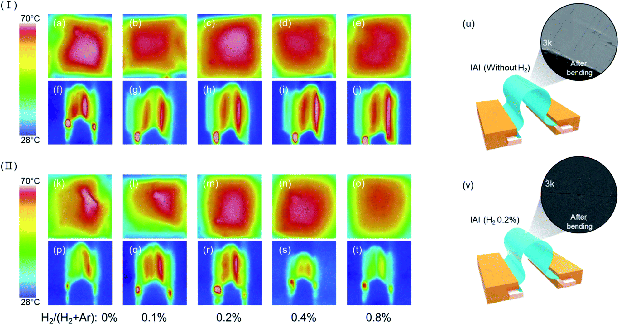 | ||
| Fig. 6 The thermal images before and after dynamic bending stress of IAI:H multi-structure are shown. The (I) shows thermal images of before 5000 cycles bending test with (a)–(e) flat state and (f)–(j) bended state. And the (II) shows thermal images of after 5000 cycles bending test with (k)–(o) flat state and (p)–(t) bending state. The schematic of microcrack formation and SEM images after 5000 cycles bending test on top layer (u) without hydrogen and (v) with hydrogen flow 0.2%. Numerous microcracks are observed on the surface of IAI without hydrogen, whereas, IAI:H shows obvious difference. | ||
Conclusions
A hybrid structure consisting of OMO has high electrical, optical, and mechanical properties, but the mechanical properties encounter problems because of the polycrystalline structure of the top oxide layer formed on the polycrystalline metal layer. In this work, we introduced hydrogen to the top and bottom ITO layers for mechanical stability improvement. The hydrogen presence in the IAI:H structure and stabilized amorphous oxide structure was confirmed. The mechanical stability was dramatically improved with a 0.2% hydrogen flow ratio, and low residual stress and average change in resistance were demonstrated. The electrical property changes before and after dynamic bending testing revealed the reason why there was a decrease in electrical property. Generally, the ρ of ITO depends on the n due to ionization scattering,47 but in this case, the μ determined the ρ of the multistructure du to microcrack formation on the surface. The improved mechanical stability was confirmed with heat thermal emissivity and heated temperature before and after dynamic bending testing. As a result, the correct amount of hydrogen can produce a stabilized amorphous structure simply. This result implies that multistructures that contain unintended polycrystalline can be stabilized with hydrogen introduction.Conflicts of interest
The authors declare that they have no conflict of interest.Acknowledgements
This work was partly supported by Basic Science Research Program through the National Research Foundation of Korea (NRF) funded by the Ministry of Education (2019R1A6A3A01091664) and by the Technology Development Program of MSS (S2780957) and by the Ministry of the Environment (G232019012551).References
- H. Hosseinzadeh Khaligh, K. Liew, Y. Han, N. M. Abukhdeir and I. A. Goldthorpe, Sol. Energy Mater. Sol. Cells, 2015, 132, 337–341 CrossRef CAS.
- M. H. Ahn, E. S. Cho and S. J. Kwon, Appl. Surf. Sci., 2011, 258, 1242–1248 CrossRef CAS.
- Y. Nakayama and S. Akita, Synth. Met., 2001, 117, 207–210 CrossRef CAS.
- J. Y. Lee, S. T. Connor, Y. Cui and P. Peumans, Nano Lett., 2010, 10, 1276–1279 CrossRef CAS.
- J. Wu, M. Agrawal, H. A. Becerril, Z. Bao, Z. Liu, Y. Chen and P. Peumans, ACS Nano, 2010, 4, 43–48 CrossRef CAS.
- A. Khan, S. Lee, T. Jang, Z. Xiong, C. Zhang, J. Tang, L. J. Guo and L. Wen-Di, Small, 2016, 12, 3021–3030 CrossRef CAS.
- G. Khanarian, J. Joo, X. Q. Liu, P. Eastman, D. Werner, K. O’Connell and P. Trefonas, J. Appl. Phys., 2013, 114(2), 024302 CrossRef.
- K. Miyaura, Y. Miyata, B. Thendie, K. Yanagi, R. Kitaura, Y. Yamamoto, S. Arai, H. Kataura and H. Shinohara, Sci. Rep., 2018, 8, 2–7 CrossRef.
- I. Hamberg and C. G. Granqvist, J. Appl. Physiol., 1986, 60, R123 CrossRef CAS.
- K. Rana, J. Singh and J. H. Ahn, J. Mater. Chem. C, 2014, 2, 2646–2656 RSC.
- H. Wu, D. Kong, Z. Ruan, P. C. Hsu, S. Wang, Z. Yu, T. J. Carney, L. Hu, S. Fan and Y. Cui, Nat. Nanotechnol., 2013, 8, 421–425 CrossRef CAS.
- T. Sannicolo, M. Lagrange, A. Cabos, C. Celle, J. P. Simonato and D. Bellet, Small, 2016, 12, 6052–6075 CrossRef CAS.
- W. G. Haines and R. H. Bube, J. Appl. Phys., 1978, 49, 304–307 CrossRef CAS.
- F. O. Adurodija, L. Semple and R. Brüning, J. Mater. Sci., 2006, 41, 7096–7102 CrossRef CAS.
- Y. S. Jung, J. Y. Seo, D. W. Lee and D. Y. Jeon, Thin Solid Films, 2003, 445, 63–71 CrossRef CAS.
- P. C. Chen, G. Shen, H. Chen, Y. G. Ha, C. Wu, S. Sukcharoenchoke, Y. Fu, J. Liu, A. Facchetti, T. J. Marks, M. E. Thompson and C. Zhou, ACS Nano, 2009, 3, 3383–3390 CrossRef CAS.
- J. W. Kang, W. I. Jeong, J. J. Kim, H. K. Kim, D. G. Kim and G. H. Lee, Electrochem. Solid-State Lett., 2007, 10, 75–78 CrossRef.
- Y. Leterrier, L. Médico, F. Demarco, J. A. E. Månson, U. Betz, M. F. Escolà, M. K. Olsson and F. Atamny, Thin Solid Films, 2004, 460, 156–166 CrossRef CAS.
- Z. Chen, B. Cotterell, W. Wang, E. Guenther and S. J. Chua, Thin Solid Films, 2001, 394, 201–205 CrossRef.
- D. Y. Lee, J. R. Lee, G. H. Lee and P. K. Song, Surf. Coat. Technol., 2008, 202, 5718–5723 CrossRef CAS.
- G. S. Heo, Y. Matsumoto, I. G. Gim, H. K. Lee, J. W. Park and T. W. Kim, Solid State Commun., 2010, 150, 223–226 CrossRef CAS.
- H. K. Park, J. A. Jeong, Y. S. Park, H. K. Kim and W. J. Cho, Thin Solid Films, 2009, 517, 5563–5568 CrossRef CAS.
- S. K. Hau, H. L. Yip, J. Zou and A. K. Y. Jen, Org. Electron., 2009, 10, 1401–1407 CrossRef CAS.
- J. H. Chang, K. M. Chiang, H. W. Kang, W. J. Chi, J. H. Chang, C. I. Wu and H. W. Lin, Nanoscale, 2015, 7, 4572–4579 RSC.
- D. Y. Choi, H. W. Kang, H. J. Sung and S. S. Kim, Nanoscale, 2013, 5, 977–983 RSC.
- D. S. Hecht, L. Hu and G. Irvin, Adv. Mater., 2011, 23, 1482–1513 CrossRef CAS.
- Q. Pei, G. Zuccarello, M. Ahlskog and O. Inganäs, Polymer, 1994, 35, 1347–1351 CrossRef CAS.
- J. Kim, S. Kim, S. Yoon and P. Song, J. Opt. Soc. Korea, 2016, 20, 807–812 CrossRef CAS.
- S. H. Kim, S. H. Kim and P. K. Song, J. Korean Inst. Met. Mater., 2017, 55, 581–586 CAS.
- P. Zhao, S. Kim, S. Yoon and P. Song, Thin Solid Films, 2018, 665, 137–142 CrossRef CAS.
- M. Girtan, Sol. Energy Mater. Sol. Cells, 2012, 100, 153–161 CrossRef CAS.
- K. H. Choi, H. J. Nam, J. A. Jeong, S. W. Cho, H. K. Kim, J. W. Kang, D. G. Kim and W. J. Cho, Appl. Phys. Lett., 2008, 92, 2–5 Search PubMed.
- M. Bender, W. Seelig, C. Daube, H. Frankenberger, B. Ocker and J. Stollenwerk, Thin Solid Films, 1998, 326, 67–71 CrossRef CAS.
- K. H. Choi, J. Y. Kim, Y. S. Lee and H. J. Kim, Thin Solid Films, 1999, 341, 152–155 CrossRef CAS.
- J. A. Jeong, Y. S. Park and H. K. Kim, J. Appl. Phys., 2010, 107, 023111 CrossRef.
- K. Hong, K. Kim, S. Kim, I. Lee, H. Cho, S. Yoo, H. W. Choi, N. Y. Lee, Y. H. Tak and J. L. Lee, J. Phys. Chem. C, 2011, 115, 3453–3459 CrossRef CAS.
- J. C. C. Fan, F. J. Bachner, G. H. Foley and P. M. Zavracky, Appl. Phys. Lett., 1974, 25, 693–695 CrossRef CAS.
- J. A. Jeong and H. K. Kim, Sol. Energy Mater. Sol. Cells, 2009, 93, 1801–1809 CrossRef CAS.
- C. Guillén and J. Herrero, Opt. Commun., 2009, 282, 574–578 CrossRef.
- Y. S. Park, K. H. Choi and H. K. Kim, J. Phys. D: Appl. Phys., 2009, 42, 235109 CrossRef.
- K. P. Sibin, G. Srinivas, H. D. Shashikala, A. Dey, N. Sridhara, A. Kumar Sharma and H. C. Barshilia, Sol. Energy Mater. Sol. Cells, 2017, 172, 277–284 CrossRef CAS.
- T. C. Gorjanc, D. Leong, C. Py and D. Roth, Thin Solid Films, 2002, 413, 181–185 CrossRef CAS.
- Y.-S. Park, H.-K. Park, J.-A. Jeong, H.-K. Kim, K.-H. Choi, S.-I. Na and D.-Y. Kim, J. Electrochem. Soc., 2009, 156, H588 CrossRef CAS.
- Y. S. Kim, J. H. Park, D. H. Choi, H. S. Jang, J. H. Lee, H. J. Park, J. I. Choi, D. H. Ju, J. Y. Lee and D. Kim, Appl. Surf. Sci., 2007, 254, 1524–1527 CrossRef CAS.
- S. han Kim, J. Yoon, S. H. Jin, J. Bang and P. Song, Coatings, 2019, 9, 11–15 Search PubMed.
- S. Kim, J. hee Yoon, J. Bang and P. Song, Thin Solid Films, 2019, 669, 275–280 CrossRef CAS.
- T. Sasabayashi, N. Ito, E. Nishimura, M. Kon, P. K. Song, K. Utsumi, A. Kaijo and Y. Shigesato, Thin Solid Films, 2003, 445, 219–223 CrossRef CAS.
- Y. C. Lin, J. Y. Li and W. T. Yen, Appl. Surf. Sci., 2008, 254, 3262–3268 CrossRef CAS.
- D. H. Zhang and H. L. Ma, Appl. Phys. A: Mater. Sci. Process., 1996, 62, 487–492 CrossRef.
| This journal is © The Royal Society of Chemistry 2021 |