
 Open Access Article
 This Open Access Article is licensed under a Creative Commons Attribution-Non Commercial 3.0 Unported Licence
Controllable synthesis of non-layered two-dimensional plate-like CuGaSe2 materials for optoelectronic devices†
Wenling Feng,
Yutong Zhao,
Di Zhao,
Wenjian Wang,
Zenghao Xia,
Xiaoxia Zheng,
Xu Wang,
Weihua Wang and
Wenliang Wang *
*
School of Chemistry and Chemical Engineering, Qufu Normal University, Qufu 273165, Shandong, P. R. China. E-mail: wlwang@qfnu.edu.cn; Tel: +86-1565-023-5536
First published on 18th January 2021
Abstract
CuGaSe2 semiconductor materials, as an important member of the I–III–VI2 family, have sparked tremendous attention due to their fascinating structure-related properties and promising applications in solar energy storage and conversion. Nevertheless, the controllable preparation of two-dimensional (2D) CuGaSe2 structures is still a daunting challenge owing to the intrinsic non-layered crystal structure and inaccessible reactivity-matching of multiple reaction precursors, which will seriously impede the much deeper research progress on their properties and applications. Herein, non-layered 2D CuGaSe2 plates possessing high crystallinity, and uniform size and morphology have been first synthesized by a feasible cation exchange strategy. Because the fabrication of 2D CuGaSe2 crystals is rarely reported, a particular highlight is laid on the compositional analysis, structural characterization, and formation mechanism. Furthermore, the optical absorption and optoelectronic measurements reveal that the as-synthesized CuGaSe2 plates exhibit high light harvesting capacity and excellent photoelectric performance. This study opens up a new avenue for the feasible fabrication of non-layered CuGaSe2 plates possessing a high-quality crystalline structure and provides a promising candidate for the development of novel solar energy conversion and storage devices.
1. Introduction
Since the first successful synthesis of graphene in 2004,1 two-dimensional (2D) materials have aroused the great interest and enthusiasm of researchers owing to their high specific surface area, unique electronic structure and excellent physical and chemical properties.2–4 Generally, 2D materials can be divided into layered and non-layered types according to their crystal structures. Despite the fact that previous work mainly focused on 2D materials with a layered crystal structure, the research on 2D non-layered materials has gradually attracted extensive attention.5–7 Importantly, the emergence and development of 2D non-layered semiconductor structures plays a vital role in broadening and deepening the fundamental investigation on 2D materials, which also exhibit intriguing structure- and composition-dependent physicochemical properties and advanced applications.8–10 Compared with layered materials, non-layered 2D crystals feature abundant dangling bonds on the surface and intrinsic crystal distortion that render them specially promising applications in solar energy conversion and storage, such as photovoltaic cells, optoelectronic detection, and photocatalytic fields.6,11–13 Solar energy, featuring its universality, inexhaustibility, environmental benignity and high capacity, is identified as the most promising option for renewable energy. Accordingly, developing advanced materials to efficiently convert solar energy into chemical and/or electronic energy is attracting great research interest. In particular, 2D semiconductor materials originating from their unique physical, electronic, and structural properties have been intensively investigated for application in electronic and optoelectronic devices.5 To date, considerable efforts have been made to achieve the anisotropic growth on non-layered materials.6 However, the most studies of these 2D structures have largely limited to binary compounds, such as CdX (X = S, Se, Te)14–16 and PbX (X = S, Se).17 In addition, further applications of these materials are severely restricted by the inherent toxicity of Cd and Pb. Strikingly, as the potential alternatives to the CdX or PbX crystals, copper-based chalcogenide compounds have spawned growing interest and research owing to their promising applications in optoelectronic devices.18–20 Therefore, rational design a facile approach for the controllable fabrication of 2D non-layered semiconductor materials with appropriate bandgap energy, low toxicity and high light absorption coefficient is of great significance for improving conversion of solar energy into chemical and/or electronic energy.Currently, accumulating evidences demonstrate that copper-based ternary I–III–VI2 (I = Cu; III = Ga, In; VI = S, Se, Te) chalcogenide semiconductor materials have received a great deal of attention due to their distinct composition and structure-tunable properties and extensive applications.21–31 For instance, Wang et al. reported a hot injection method for the preparation of monodispersed wurtzite structure CuInSe2 nanocrystals with uniform hexagonal shape as well as their high performance in optoelectronic application.32 Xia et al. demonstrated a solvothermal synthesis technique to prepare CuInS2 quantum dots and studied their size-dependent optical properties.33 Among these I–III–VI2 materials, CuGaSe2 as a typical p-type semiconductor possesses an appropriate bandgap and high light absorption coefficient, which makes it as an ideal effective light-absorbing material in optoelectronic and photovoltaic applications.18,34–36 Over the past several years, tremendous endeavors have been devoted to develop synthetic strategies for controllable preparation of CuGaSe2 materials, and significant advances have been achieved. For example, Tang et al. prepared CuGaSe2 nanocrystals using a hot injection method.34 Feng et al. developed a solid-state reaction to synthesize CuGaSe2 nanocrystals.18 Nevertheless, the morphology of the as-prepared CuGaSe2 materials is mostly restricted in the form of nanoparticles, which may heavily hamper their potential applications in optoelectronic devices. In sharp contrast to the synthesis of binary chalcogenides, there is still a big challenge to control the composition, shape, and crystal phase of ternary nanocrystals due to the difficult to balance the reactivity of three different precursors to favor the formation of ternary compound and restrain binary by-products.29,37 To date, the controllable preparation of 2D CuGaSe2 crystals through wet-chemical methods is still in its infancy. Especially, tetragonal phase 2D CuGaSe2 structures with high crystalline quality and uniform size have rarely been reported.18 Consequently, exploring and developing a feasible synthesis method for controlled preparation of tetragonal phase 2D CuGaSe2 materials is urgently needed, which will further deepen the understanding of the growth mechanism and promote comprehensive applications of 2D non-layered materials.
Cation exchange reactions, in which involve replacing cations of a parent crystalline structure with diverse metal ions.38,39 Cation exchange method has been demonstrated to be an extremely efficient strategy in the colloid synthesis of semiconductor materials with unique composition, morphology, and crystal structure that are difficult to be achieved by simple direct growth methods.40–44 For example, Berends et al. synthesized CuInSe2 quantum dots, nanoplatelets, and nanosheets by partial indium-cation exchange into Cu2−xSe nanocrystals.45 Wang et al. reported the successful conversion of layered SnS2 into nonlayered 2D Cu2SnS3 nanosheets via cation exchange.46 Ramirez et al. demonstrated a morphology transformation from Cu2−xSe nanoparticles to Cu3SbSe3 nanoplates by cation exchange reactions.20 Such convincing evidences indicate that cation exchange reaction may offer an effective approach for the preparation of tetragonal phase 2D CuGaSe2 structures.
In this work, we demonstrate for the first time a partial cation exchange strategy to prepare tetragonal phase 2D CuGaSe2 plates. Firstly, Cu2−xSe plates are synthesized via a hot-injection method. Subsequently, Ga3+ ions are incorporated into the Cu2−xSe crystal lattice via the partial replacement of Cu+ by Ga3+. The shape and size of the parent Cu2−xSe without obvious change is retained in resulting CuGaSe2 crystals. The phase purity of the synthesized CuGaSe2 plates can be regulated by varying the initial precursor Ga![[thin space (1/6-em)]](https://www.rsc.org/images/entities/char_2009.gif) :Cu ratio. On the basis of systematic analysis by several characterization techniques, a possible formation mechanism of CuGaSe2 plates has been proposed. Moreover, optoelectronic measurements confirm that a photodetector based on the CuGaSe2 plates exhibits excellent sensitivity and stability.
:Cu ratio. On the basis of systematic analysis by several characterization techniques, a possible formation mechanism of CuGaSe2 plates has been proposed. Moreover, optoelectronic measurements confirm that a photodetector based on the CuGaSe2 plates exhibits excellent sensitivity and stability.
2. Experimental section
2.1 Materials
Gallium (III) acetylacetonate (Ga(acac)3, 99.99%) and diphenyl diselenide (Ph2Se2, 98%) were purchased from Alfa Aesar. Octadecene (ODE, 90%) and oleylamine (OAm, 70%) were ordered from Sigma-Aldrich. Oleic acid (OA), anhydrous copper chloride (CuCl), absolute ethanol, and toluene were purchased from Sinopharm Chemical Reagent Ltd., China. All chemicals were used directly without further purification.2.2 Preparation of Se–ODE and Ga–OAm precursors
The Se–ODE precursor solution was prepared by addition of 0.0624 g of Ph2Se2 (0.2 mmol) to 1.0 mL of ODE, followed by heating to 70 °C, yielding a transparent orange liquid.47 The Ga–OAm precursor solution was prepared in a nitrogen atmosphere, by dissolving 0.3670 g of Ga(acac)3 (1.0 mmol) in 10.0 mL OAm in a three-neck flask under magnetic stirring, followed by heating to 120 °C for 60 min until the Ga(acac)3 absolutely dissolved.482.3 Synthesis of the two-dimensional CuGaSe2 plates
CuGaSe2 plates were prepared according to our previously reported method with a slight modification.49 In a typical synthesis procedure, 0.0099 g of CuCl (0.10 mmol) together with 0.2 mL of OAm, 0.2 mL of OA and 6.0 mL of ODE were brought into a three-neck round-bottom flask (100 mL) at room temperature. In order to eliminate dissolved oxygen, adventitious water and other low-boiling-point impurities, the mixture was first heated to 130 °C and maintained for 30 min under nitrogen atmosphere and constant stirring. After that, the reaction mixture was further heated to 230 °C. At this point, the Se–ODE precursor solution was transferred into a syringe equipped with a large needle and injected quickly into the flask at 230 °C and kept at the temperature for 10 min. Subsequently, 2.0 mL Ga–OAm precursor solution was immediately injected into the above solution and the reaction mixture was further raised to 255 °C and maintained for 90 min with continuous stirring. After the reaction was complete, the resulting solution was allowed to cool to room temperature naturally. The as-synthesized product was collected by centrifugation (9000 rpm, 3 min) and washed several times with absolute ethanol and toluene.2.4 Characterization
The as-prepared samples were characterized by X-ray diffraction (XRD) performed on a Philips X'pert PRO X-ray diffractometer (Cu Kα, λ = 1.54182 Å). The morphologies of the samples were examined using a Scanning Electron Microscopy (SEM, JSM-6700F). The high resolution transmission electron microscopy (HRTEM), selected area electron diffraction (SAED) patterns, high-angle annular dark-field scanning transmission electron microscopy (HAADF-STEM), and corresponding energy-dispersive X-ray spectroscope (EDX) mapping analyses were performed on a JEOL JEM-ARF200F TEM/STEM with a spherical aberration corrector. Inductively Coupled Plasma Atomic Emission Spectroscopy (ICP-AES) analysis was performed on a PerkinElmer Model Optima 3000DV to quantify the copper, gallium, and selenium content of the resulting crystals. X-ray Photoelectron Spectroscopy (XPS) was performed using an ESCALAB MK II with Mg Kα as the excitation source. The ultraviolet-visible-near infrared (UV-vis-NIR) absorption spectra were recorded on a spectrophotometer (Shimadzu Solidspec-3700DUV) at room temperature. The samples were prepared by dispersing the plates in toluene. Thermogravimetric analysis (TGA) was performed on a STA-449-F3 thermal analyzer (NETZSCH Corporation) with a heating rate of 10 °C min−1 in flowing argon. Current–voltage (I–V) characteristics of the devices were recorded with a two-probe method using an electrochemical station (CHI660e) and xenon lamp (PLS-SXE300) was selected as a white light source.3. Results and discussion
3.1 Characterizations of the CuGaSe2 plates
The typical CuGaSe2 plates have been synthesized by means of a cation exchange method. The method consists of a sequential two-step strategy, i.e., starting from the as-synthesized Cu2−xSe plates followed by the incorporation of Ga3+ via an in situ cation exchange reaction, leading to homogeneous CuGaSe2 plates. The structure, morphology, and composition of the as-obtained CuGaSe2 plates are comprehensively characterized by various techniques. As shown in Fig. 1a, the crystal structure of the as-prepared CuGaSe2 plates is characterized by the powder XRD. The major specific diffraction peaks at 27.7°, 45.7°, 46.1°, 54.2°, and 55.0° can be respectively indexed to the (112), (220), (204), (312), and (116) planes of the tetragonal chalcopyrite phase of CuGaSe2 (JCPDS no. 31-0456).36 The none-existence of any observable impurity peak and peak splitting can confirm the absence of the chance of the phase separation during the synthesis of CuGaSe2 plates. Meanwhile, the presence of strong and sharp diffraction peaks verifies the highly crystalline nature of the resulting CuGaSe2 plates. The morphology of CuGaSe2 crystals is examined by SEM measurement. As displayed in Fig. 1b, it can be seen that the as-synthesized CuGaSe2 crystals are roughly hexagonal structure. The thickness and edge length of the CuGaSe2 plates are around 45.3 ± 2.3 nm and 328.1 ± 17.6 nm (Fig. S1 of the ESI†), respectively. HRTEM, SAED, and EDX are performed to investigate the crystal microstructure and composition of the resultant CuGaSe2 plates. As shown in Fig. 1c, the lattice fringes can be clearly observed, uncovering the well-defined single-crystalline structure. Moreover, the detected interplanar distances of the CuGaSe2 plates are 0.32 and 0.20 nm, which can be assigned to the (112) and (2−20) lattice planes of tetragonal phase CuGaSe2,18,50 respectively. For the corresponding SAED pattern depicted in Fig. 1d, the observed regular symmetric diffractions can also demonstrate that the as-prepared CuGaSe2 plates possess good crystallinity. In addition, the elemental composition of CuGaSe2 plates is determined by EDX. As detected in Fig. S2,† the corresponding Cu:Ga:Se atomic ratio is close to 1:1:2, which is consistent with the ICP-AES analysis (Table S1 of the ESI†). All of the above measurement results confirm that as-prepared CuGaSe2 plates are of high purity and good crystalline structure.
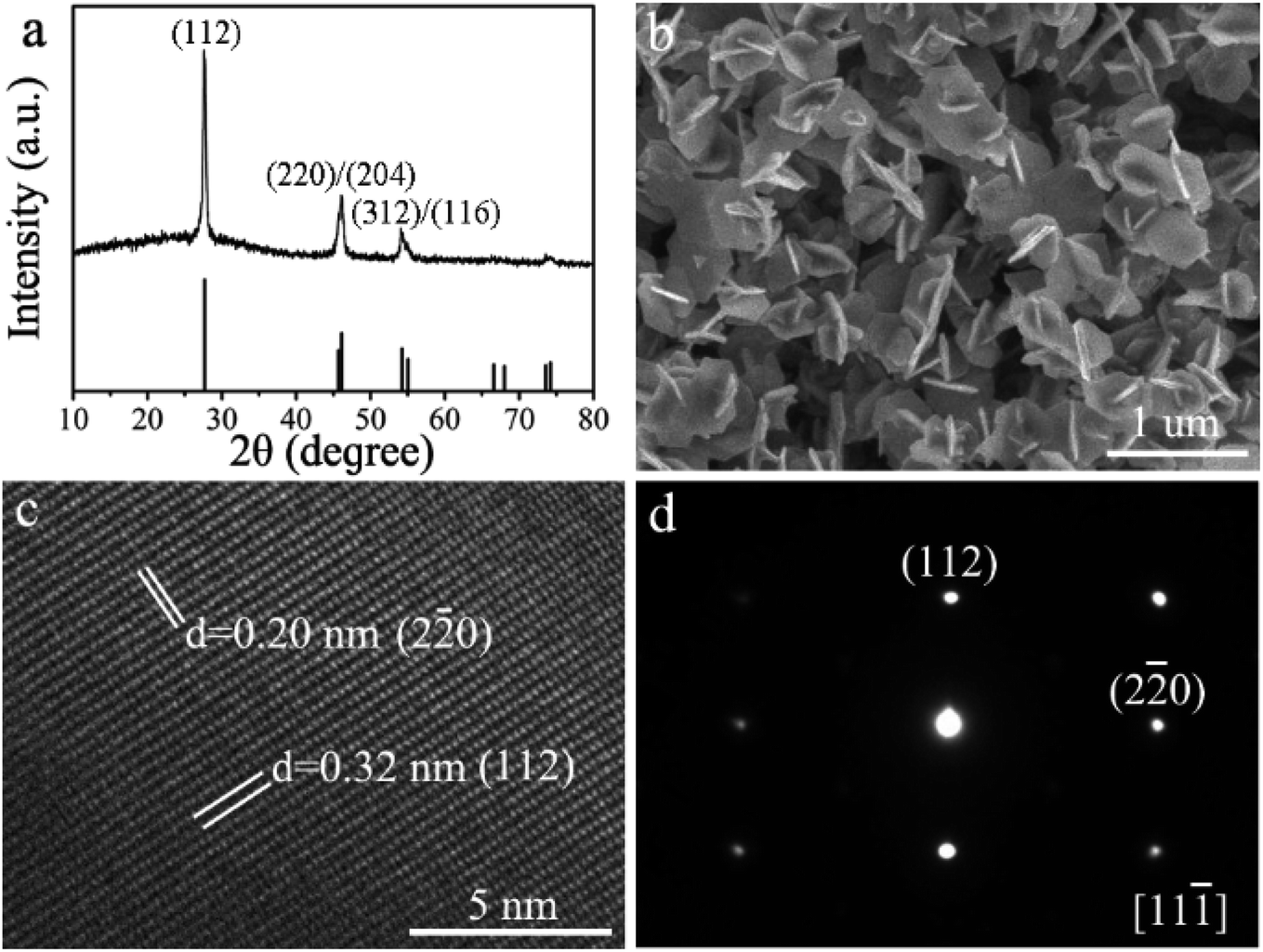 | ||
| Fig. 1 (a) XRD pattern along with standard JCPDS no. 31-0456 for reference and (b) SEM image of the as-synthesized CuGaSe2 plates. (c) HRTEM image and (d) the corresponding SAED pattern of the CuGaSe2 plates. | ||
In order to further verify the structure and composition of the CuGaSe2 plates, STEM-EDX analysis was conducted. As shown in Fig. 2a, STEM image demonstrates a good consistent with the SEM observation, in which the prepared CuGaSe2 plates are of approximately hexagonal morphology. As shown in Fig. S2 of the ESI,† the EDX measurement confirms that the resulting products are composed of Cu, Ga, and Se elements. The atomic ratio of Cu:Ga:Se is close to 1:1:2, which is well consistent with the stoichiometric ratio of CuGaSe2. In addition, as shown in Fig. 2b–d, STEM-EDX elemental mapping of the as-synthesized CuGaSe2 plates further reveals that three elements are homogeneously distributed in the plates.
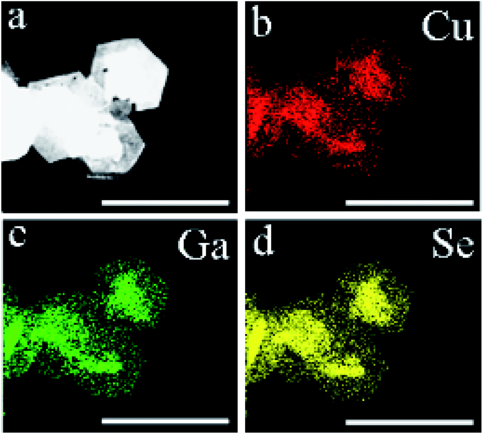 | ||
| Fig. 2 (a) HAADF-STEM image of the as-prepared CuGaSe2 plates and the corresponding STEM-EDX elemental mappings for (b) Cu, (c) Ga and (d) Se, respectively. The scale bar is 1 μm. | ||
X-ray photoelectron spectroscopy (XPS) has been performed to investigate the chemical state and elemental composition of the synthesized CuGaSe2 plates. As illustrated in Fig. 3a, the XPS survey spectrum uncovers the existence of Cu, Ga, Se, C, and O in the resulting CuGaSe2 plates. As shown in Fig. 3b the copper high-resolution XPS spectrum, two characteristic peaks of Cu 2p3/2 and Cu 2p1/2 locating at 931.5 and 951.3 eV with a peak splitting of 19.8 eV demonstrate the presence of Cu(I) in the CuGaSe2 plates.51 The gallium high-resolution XPS spectrum in Fig. 3c exhibits two peaks at 1143.6 and 1116.7 eV corresponding to Ga 2p1/2 and Ga 2p3/2,52,53 respectively, suggesting that the chemical state of the Ga in the composite is +3. In Fig. 3d the high-resolution XPS spectrum of Se 3d, the two peaks of 53.2 and 54.1 eV are assigned to Se 3d5/2 and Se 3d3/2, respectively, indicating the −2 oxidation state of Se in the as-prepared CuGaSe2 plates.54 Consequently, XPS results further verify that CuGaSe2 plates without any other impurities have been successfully prepared.
 | ||
| Fig. 3 XPS spectra of the as-prepared CuGaSe2 plates. (a) Survey spectrum, (b) Cu 2p core level spectrum, (c) Ga 2p core level spectrum, and (d) Se 3d core level spectrum. | ||
3.2 Formation mechanism of the CuGaSe2 plates
To gain a further insight into the formation mechanism of the as-prepared CuGaSe2 plates, the products of different reaction stages before and after gallium precursor injection have been carefully investigated. Firstly, we will analyze the results of reaction system before injecting gallium precursor. In the first step, the crystal structure, chemical composition, and morphology of the resulting crystals after injecting selenium precursor at 230 °C for 10 min (Experimental section for details) are characterized by several techniques. The SEM image in Fig. 4 depicts the synthesized crystals are of fairly uniform plates. The thickness and edge length of the plates are around 43.8 ± 2.9 nm and 320.5 ± 15.8 nm (Fig. S3†), respectively. As seen in Fig. S4,† the interplanar distance of 0.33 nm can be well indexed to the (111) lattice space of the cubic Cu2−xSe.55 The crystal phase of the resulting product is characterized by XRD. As shown in Fig. 5a, the emerged diffraction peaks at 27.0°, 31.3°, 44.8°, 53.1°, 65.2°, and 71.9° can be assigned to the (111), (200), (220), (311), (400), and (331) planes of the cubic phase of Cu2−xSe (JCPDS no. 06-0680),55 respectively. Furthermore, EDX analysis in Fig. 5b demonstrates that as-prepared Cu2−xSe crystals have Cu deficient stoichiometry with the Cu:Se ratio of 1.85:1. Strikingly, slightly Cu-deficient composition of Cu2−xSe crystals is favorable for cation exchange reactions.56 XPS analysis is conducted to probe surface chemistry of prepared Cu2−xSe plates. For the high-resolution XPS spectrum of Cu 2p in Fig. 5c, the peaks at 932.0 (2p3/2) and 951.8 eV (2p1/2) demonstrate the presence of Cu+.57 Fig. 5d displays the high-resolution XPS spectrum of Se 3d, where the peaks at 53.8 (3d5/2) and 54.3 (3d3/2) eV indicate the (−2) oxidation state of Se.58 Overall, these experimental results can verify the formation of cubic Cu2−xSe plates prior to the injection of gallium precursor.
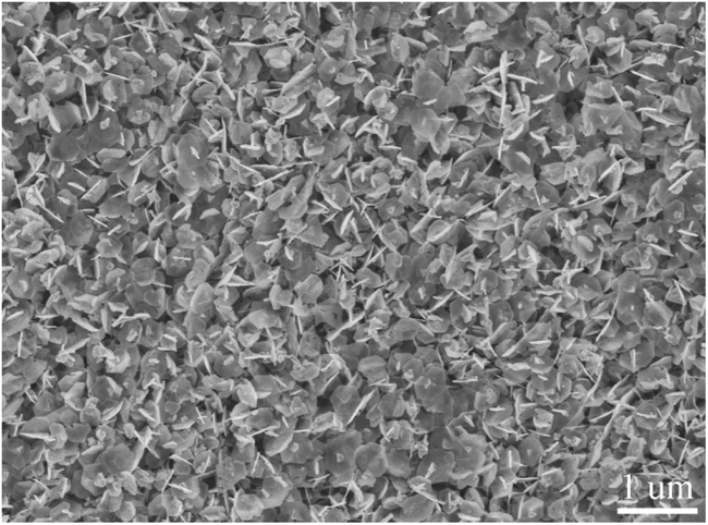 | ||
| Fig. 4 SEM image of the sample synthesized at 230 °C for 10 min after Se-precursor injection. | ||
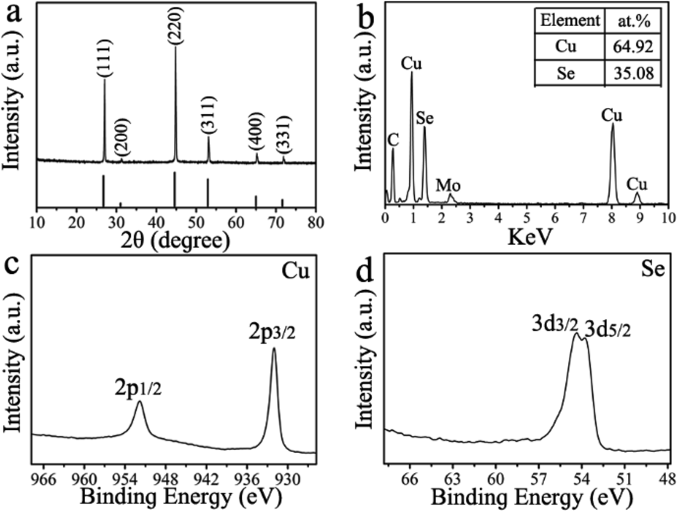 | ||
| Fig. 5 (a) XRD pattern, (b) EDX spectrum, XPS spectra of (c) Cu 2p core level and (d) Se 3d core level of the product synthesized at 230 °C for 10 min after Se-precursor injection. | ||
The synthesized Cu2−xSe plates remained in the crude solution for the following cation exchange reaction toward CuGaSe2 plates. Generally, high temperature is favorable to impel the proceeding of cation exchange reactions for the synthesis of Ga-containing nanomaterials.23 In addition, it is worth noting that molar ratio of precursors is judiciously controlled since it has a significant effect on the phase purity of the resulting product. We raise the reaction temperature to 255 °C after injecting gallium precursor. The XRD characterizations have been employed to monitor the phase evolution of the resulting products obtained from various Ga:Cu precursor molar ratios during the process of cation exchange reactions. As shown in Fig. 6a and b, a group of XRD patterns reveal that the initial cubic phase Cu2−xSe has partially transformed into tetragonal phase CuGaSe2 when the Ga:Cu ratio changes from 0:1 to 1:1. Further increase of the Ga:Cu ratio up to 1.5:1 in Fig. 6c results in the enhancement of the representative diffraction peaks at 27.7°, 46.1°, and 54.2°, which can be indexed to the (112), (220)/(204), and (312)/(116) planes of the tetragonal chalcopyrite phase of CuGaSe2. Meanwhile the fading of the main characteristic peaks at 27.0°, 44.8°, and 53.1° matched with the (111), (220), and (311) planes of cubic Cu2−xSe. Finally, as present in Fig. 6d, a pure tetragonal structure of CuGaSe2 plates with nearly hexagonal shape is successfully achieved when the Ga:Cu ratio increases to 2:1. It is demonstrated that CuGaSe2 plates with desired stoichiometric combination can be obtained by suitable adjustment of molar precursor ratios.
 | ||
| Fig. 6 XRD patterns of the samples synthesized with different precursor molar ratios: (a) Ga:Cu = 0, (b) Ga:Cu = 1, (c) Ga:Cu = 1.5, (d) Ga:Cu = 2. | ||
3.3 Optical and optoelectronic properties of the CuGaSe2 plates
To prove the ability of the optoelectronic device application of the CuGaSe2 plates, UV-vis-NIR absorption spectra are measured to investigate the optical properties. As depicted in Fig. 7a, an obvious comparison in absorption curves can be observed between Cu2−xSe and CuGaSe2 crystals. The spectral response curve of initial Cu2−xSe plates exhibits two stages. For the ranges within 800 nm, they should be induced by excitonic or interband transitions. However, the range beyond 800 nm, they should be caused by localized surface plasmon resonance (LSPR). Remarkably, a distinct LSPR of Cu2−xSe plates in the NIR region arising from the copper-defect-induced free carriers is thoroughly restrained after the partial replacement of Cu+ with Ga3+ via cation exchange reactions. Such results of UV-vis-NIR absorption demonstrate another evidence of the successful transformation from Cu2−xSe to CuGaSe2. Meanwhile, the as-synthesized CuGaSe2 plates demonstrate a stronger absorption in visible light region. On the base of absorption spectra, the direct optical bandgap energy of CuGaSe2 plates in Fig. 7b is determined by extrapolation of the linear region of the Tauc plot to the photon energy. As a result, the calculated bandgap is 1.61 ± 0.003 eV (Fig. S5†), which is in well consistent with the literature report.59 Moreover, we have investigated the thermal stability of the resulting CuGaSe2 plates. According to TG analysis in Fig. S6,† the small amount of weight loss over the temperature range from 100 to 380 °C may be attributed to the removal of absorbed water molecules and some organic compounds on the materials' surface. With the increase of the temperature, up to about 530 °C, the CuGaSe2 plates will be further decomposed. Based on the above results of TGA, we suggest that the synthesized CuGaSe2 plates have good thermal stability. | ||
| Fig. 7 (a) UV-vis-NIR absorption spectra of Cu2−xSe and CuGaSe2 plates dispersed in toluene. (b) The linear extrapolations of plots of (αhν)2 vs. photon energy. (c) Current versus voltage curves of the CuGaSe2 plates measured in dark and under xenon lamp illumination with a power intensity of 6.5 mW cm−2, and (d) current versus time curves during ON and OFF cycles. | ||
Based on the above results of absorption spectra, the synthesized CuGaSe2 plates are expected as promising light-harvesting materials for optoelectronic applications. To further evaluate the potential application of CuGaSe2 plates in optoelectronics, a photodetector is constructed by drop-casting a concentrated toluene solution of CuGaSe2 plates onto glass substrate and employed two adjacent ITO film as conductive electrodes.51 A xenon lamp is utilized as a white light source by equipped with a cutoff filter of 400 nm, which can afford visible light ranging from 400 to 780 nm.
Fig. 7c shows the current–voltage (I–V) curves of the CuGaSe2 plates photodetector measured in the dark and under light illumination at a bias of 1.0 V, respectively. The linear curves demonstrate good ohmic contacts between the ITO electrodes and CuGaSe2 plates. In addition, it is obviously observed that the current under light illumination is higher than that in the case of dark. The stability and responsivity are also identified as key factors to assess the property of a photodetector. For purpose of exploring the stability and responsivity of the CuGaSe2-based photodetector, the time-dependent current response has been conducted under illumination with light intensity of 6.5 mW cm−2 at a voltage of 1.0 V. Fig. 7d exhibits the photocurrents of the device during repetitive switching of light illumination, or on/off switching. The photocurrent increases and decreases as a response to the periodically switching on and off operation for a duration of 50 s, exhibiting high sensitivity. Furthermore, the photocurrent can still be changed by periodically turning on and off the light even though after a number of cycles. Such results indicate that the photodetector based on the CuGaSe2 plates has an excellent stability and repeatability.
4. Conclusions
In summary, we have first demonstrated a cation exchange method to prepare non-layered tetragonal phase 2D CuGaSe2 plates. Starting from the synthesis of Cu2−xSe plates, a subsequent cation exchange with Ga3+ results in the formation of CuGaSe2 plates while retaining their original shape and size. The phase purity of CuGaSe2 plates can be controlled by regulating the initial precursor ratio. Furthermore, we also reveal that CuGaSe2 plates have promising potential application in photoelectric conversion. Expectedly, the present synthetic methodology of CuGaSe2 plates can also be extended for the preparation of other 2D materials from non-layered structures to further explore the physicochemical properties and advanced applications.Conflicts of interest
There are no conflicts to declare.Acknowledgements
This work was supported by the National Natural Science Foundation of China (21805163), the National College Students Innovation and Entrepreneurship Training Program (201910446030), and the Qufu Normal University Innovation and Entrepreneurship Training Program for College Students (2019A004).Notes and references
- K. S. Novoselov, A. K. Geim, S. V. Morozov, D. Jiang, Y. Zhang, S. V. Dubonos, I. V. Grigorieva and A. A. Firsov, Science, 2004, 306, 666–669 CrossRef CAS.
- X. L. Li and L. J. Zhi, Chem. Soc. Rev., 2018, 47, 3189–3216 RSC.
- Y. Chen, Z. X. Fan, Z. C. Zhang, W. X. Niu, C. L. Li, N. L. Yang, B. Chen and H. Zhang, Chem. Rev., 2018, 118, 6409–6455 CrossRef CAS.
- Y. Liu, N. O. Weiss, X. D. Duan, H. C. Cheng, Y. Huang and X. F. Duan, Nat. Rev. Mater., 2016, 1, 16042 CrossRef CAS.
- P. C. Tao, S. Yao, F. Y. Liu, B. Wang, F. Huang and M. Y. Wang, J. Mater. Chem. A, 2019, 7, 23512–23536 RSC.
- F. Wang, Z. X. Wang, T. A. Shifa, Y. Wen, F. M. Wang, X. Y. Zhan, Q. S. Wang, K. Xu, Y. Huang, L. Yin, C. Jiang and J. He, Adv. Funct. Mater., 2017, 27, 1603254 CrossRef.
- Y. H. Dou, L. Zhang, X. Xu, Z. Q. Sun, T. Liao and S. X. Dou, Chem. Soc. Rev., 2017, 46, 7338–7373 RSC.
- C. L. Tan and H. Zhang, Nat. Commun., 2015, 6, 7873 CrossRef CAS.
- S. L. Zhao, Y. Wang, Q. H. Zhang, Y. F. Li, L. Gu, Z. H. Dai, S. L. Liu, Y. Q. Lan, M. Han and J. C. Bao, Inorg. Chem. Front., 2016, 3, 1501–1509 RSC.
- S. Liu, L. Xie, H. Qian, G. Y. Liu, H. Zhong and H. B. Zeng, J. Mater. Chem. A, 2019, 7, 15411–15419 RSC.
- D. Wang, W. W. Zhou, R. Zhang, J. J. Zeng, Y. Du, S. Qi, C. X. Cong, C. Y. Ding, X. X. Huang, G. W. Wen and T. Yu, Adv. Mater., 2018, 30, 1803569 CrossRef.
- X. Y. Zhang, Z. Zhang, J. Liang, Y. G. Zhou, Y. C. Tong, Y. Wang and X. X. Wang, J. Mater. Chem. A, 2017, 5, 9702–9708 RSC.
- Y. Y. Zhan, Z. B. Shao, T. H. Jiang, J. Ye, X. F. Wu, B. C. Zhang, K. Ding, D. Wu and J. S. Jie, J. Mater. Chem. A, 2020, 8, 789–796 RSC.
- B. Jin, P. Huang, Q. Zhang, X. Zhou, X. W. Zhang, L. Li, J. W. Su, H. Q. Li and T. Y. Zhai, Adv. Funct. Mater., 2018, 28, 1800181 CrossRef.
- D. D. Zhu, J. Xia, L. Wang, X. Z. Li, L. F. Tian and X. M. Meng, Nanoscale, 2016, 8, 11375–11379 RSC.
- R. Q. Cheng, Y. Wen, L. Yin, F. M. Wang, F. Wang, K. L. Liu, T. A. Shifa, J. Li, C. Jiang, Z. X. Wang and J. He, Adv. Mater., 2017, 29, 1703122 CrossRef.
- Y. Wen, Q. S. Wang, L. Yin, Q. Liu, F. Wang, F. M. Wang, Z. X. Wang, K. L. Liu, K. Xu, Y. Huang, T. A. Shifa, C. Jiang, J. Xiong and J. He, Adv. Mater., 2016, 28, 8051–8057 CrossRef CAS.
- W. Feng, W. Zheng and P. Hu, Phys. Chem. Chem. Phys., 2014, 16, 19340–19344 RSC.
- H. Liu, M. Yu, F. Qin, W. Feng and P. Hu, ACS Appl. Nano Mater., 2018, 1, 5414–5418 CrossRef CAS.
- O. Ramirez, P. Ramasamy, Y. C. Choi and J. S. Lee, Chem. Mater., 2019, 31, 268–276 CrossRef CAS.
- S. D. Deshmukh, R. G. Ellis, D. S. Sutandar, D. J. Rokke and R. Agrawal, Chem. Mater., 2019, 31, 9087–9097 CrossRef CAS.
- N. Oh, L. P. Keating, G. A. Drake and M. Shim, Chem. Mater., 2019, 31, 1973–1980 CrossRef CAS.
- S. O. Hinterding, A. C. Berends, M. Kurttepeli, M.-E. Moret, J. D. Meeldijk, S. Bals, W. van der Stam and C. de Mello Donega, ACS Nano, 2019, 13, 12880–12893 CrossRef CAS.
- H. L. Guthrey, A. G. Norman, J. Nishinaga, S. Niki, M. M. Al-Jassim and H. Shibata, ACS Appl. Mater. Interfaces, 2020, 12, 3150–3160 CrossRef CAS.
- O. Yarema, M. Yarema and V. Wood, Chem. Mater., 2018, 30, 1446–1461 CrossRef CAS.
- B. Chen, N. Pradhan and H. Zhong, J. Phys. Chem. Lett., 2018, 9, 435–445 CrossRef CAS.
- A. C. Berends, M. J. Mangnus, C. Xia, F. T. Rabouw and C. de Mello Donega, J. Phys. Chem. Lett., 2019, 10, 1600–1616 CrossRef CAS.
- F.-J. Fan, L. Wu and S.-H. Yu, Energy Environ. Sci., 2014, 7, 190–208 RSC.
- X. J. Wu, X. Huang, X. Qi, H. Li, B. Li and H. Zhang, Angew. Chem., Int. Ed., 2014, 53, 8929–8933 CrossRef CAS.
- T. Plirdpring, K. Kurosaki, A. Kosuga, T. Day, S. Firdosy, V. Ravi, G. J. Snyder, A. Harnwunggmoung, T. Sugahara and Y. Ohishi, Adv. Mater., 2012, 24, 3622–3626 CrossRef CAS.
- H. L. Hwang, H. H. Chang, P. Sharma, A. J. Letha, L. Shao, Y. Zhang and B. H. Tseng, Adv. Sci., 2016, 3, 1500196 CrossRef.
- J.-J. Wang, Y.-Q. Wang, F.-F. Cao, Y.-G. Guo and L.-J. Wan, J. Am. Chem. Soc., 2010, 132, 12218–12221 CrossRef CAS.
- C. Xia, W. Wu, T. Yu, X. Xie, C. Van Oversteeg, H. C. Gerritsen and C. de Mello Donega, ACS Nano, 2018, 12, 8350–8361 CrossRef CAS.
- J. Tang, S. Hinds, S. O. Kelley and E. H. Sargent, Chem. Mater., 2008, 20, 6906–6910 CrossRef CAS.
- C.-R. Ho, M.-L. Tsai, H.-J. Jhuo, D.-H. Lien, C.-A. Lin, S.-H. Tsai, T.-C. Wei, K.-P. Huang, S.-A. Chen and J.-H. He, Nanoscale, 2013, 5, 6350–6355 RSC.
- M. G. Panthani, V. Akhavan, B. Goodfellow, J. P. Schmidtke, L. Dunn, A. Dodabalapur, P. F. Barbara and B. A. Korgel, J. Am. Chem. Soc., 2008, 130, 16770–16777 CrossRef CAS.
- J. F. L. Lox, Z. Y. Dang, M. L. Anh, E. Hollinger and V. Lesnyak, Chem. Mater., 2019, 31, 2873–2883 CrossRef CAS.
- J. B. Rivest and P. K. Jain, Chem. Soc. Rev., 2013, 42, 89–96 RSC.
- B. C. Steimle, A. M. Fagan, A. G. Butterfield, R. W. Lord, C. R. McCormick, G. A. Di Domizio and R. E. Schaak, Chem. Mater., 2020, 32, 5461–5482 CrossRef CAS.
- S. Gupta, S. V. Kershaw and A. L. Rogach, Adv. Mater., 2013, 25, 6923–6944 CrossRef CAS.
- V. Lesnyak, C. George, A. Genovese, M. Prato, A. Casu, S. Ayyappan, A. Scarpellini and L. Manna, ACS Nano, 2014, 8, 8407–8418 CrossRef CAS.
- J. M. Hodges, K. Kletetschka, J. L. Fenton, C. G. Read and R. E. Schaak, Angew. Chem., Int. Ed., 2015, 54, 8669–8672 CrossRef CAS.
- Y. Liu, M. Liu and M. T. Swihart, J. Am. Chem. Soc., 2017, 139, 18598–18606 CrossRef CAS.
- B. J. Beberwyck, Y. Surendranath and A. P. Alivisatos, J. Phys. Chem. C, 2013, 117, 19759–19770 CrossRef CAS.
- A. C. Berends, W. van der Stam, Q. A. Akkerman, J. D. Meeldijk, J. van der Lit and C. D. Donega, Chem. Mater., 2018, 30, 3836–3846 CrossRef CAS.
- Y. X. Wang, Y. V. Morozov, M. Zhukovskyi, R. Chatterjee, S. Draguta, P. Tongying, B. Bryant, S. Rouvimov and M. Kuno, ACS Energy Lett, 2016, 1, 175–181 CrossRef CAS.
- R. L. Brutchey, Acc. Chem. Res., 2015, 48, 2918–2926 CrossRef CAS.
- T. Wang, S. S. Farvid, M. Abulikemu and P. V. Radovanovic, J. Am. Chem. Soc., 2010, 132, 9250–9252 CrossRef CAS.
- W. L. Wang, W. L. Feng, Q. Li, Y. T. Zhao, D. Zhao, Z. H. Xia, W. J. Wang, S. L. Zhang, X. X. Zheng and Z. H. Jing, Cryst. Growth Des., 2019, 19, 1226–1232 CrossRef CAS.
- J. Li, Z. G. Jin, T. Liu, J. Wang, D. L. Wang, J. Y. Lai, H. Y. Du and L. Cui, CrystEngComm, 2013, 15, 7327–7338 RSC.
- W. Wang, W. Feng, T. Ding and Q. Yang, Chem. Mater., 2015, 27, 6181–6184 CrossRef CAS.
- M. Bandi, V. Zade, S. Roy, A. N. Nair, S. Seacat, S. Sreenivasan, V. Shutthanandan, C. G. Van de Walle, H. Peelaers and C. V. Ramana, Cryst. Growth Des., 2020, 20, 1422–1433 CrossRef CAS.
- P. U. Londhe, A. B. Rohom, R. Fernandes, D. C. Kothari and N. B. Chaure, ACS Sustainable Chem. Eng., 2018, 6, 4987–4995 CrossRef CAS.
- W. L. Wang, J. Jiang, T. Ding, C. D. Wang, J. Zuo and Q. Yang, ACS Appl. Mater. Interfaces, 2015, 7, 2235–2241 CrossRef CAS.
- Y. X. Wang, M. Zhukovskyi, P. Tongying, Y. Tian and M. Kuno, J. Phys. Chem. Lett., 2014, 5, 3608–3613 CrossRef CAS.
- V. Lesnyak, R. Brescia, G. C. Messina and L. Manna, J. Am. Chem. Soc., 2015, 137, 9315–9323 CrossRef CAS.
- W. L. Wang, T. Ding, G. H. Chen, L. Zhang, Y. Q. Yu and Q. Yang, Nanoscale, 2015, 7, 15106–15110 RSC.
- W. L. Wang, L. Zhang, G. H. Chen, J. Jiang, T. Ding, J. Zuo and Q. Yang, CrystEngComm, 2015, 17, 1975–1981 RSC.
- D. W. Houck, S. V. Nandu, T. D. Siegler and B. A. Korgel, ACS Appl. Nano Mater., 2019, 2, 4673–4680 CrossRef CAS.
Footnote |
| † Electronic supplementary information (ESI) available: SEM and HRTEM of the Cu2−xSe plates. SEM, EDX spectrum, ICP-AES, UV-vis-NIR absorption spectra, and TGA of the as-synthesized CuGaSe2 plates. See DOI: 10.1039/d0ra08662b |
| This journal is © The Royal Society of Chemistry 2021 |