
 Open Access Article
 This Open Access Article is licensed under a Creative Commons Attribution-Non Commercial 3.0 Unported Licence
Chemical vapor deposition and temperature-dependent Raman characterization of two-dimensional vanadium ditelluride
Mongur Hossain *abc,
Muhammad Ahsan Iqbalbc,
Juanxia Wub and
Liming Xie*bc
*abc,
Muhammad Ahsan Iqbalbc,
Juanxia Wub and
Liming Xie*bc
aHunan Key Laboratory of Two-Dimensional Materials, State Key Laboratory for Chemo/Biosensing and Chemometrics, College of Chemistry and Chemical Engineering, Hunan University, Changsha, 410082, P. R. China. E-mail: hossain@hnu.edu.cn
bCAS Key Laboratory of Standardization and Measurement for Nanotechnology, CAS Center for Excellence in Nanoscience, National Center for Nanoscience and Technology, Beijing 100190, P. R. China. E-mail: xielm@nanoctr.cn
cUniversity of Chinese Academy of Sciences, Beijing 100049, P. R. China
First published on 12th January 2021
Abstract
Recently, ultrathin two-dimensional (2D) metallic vanadium dichalcogenides have attracted widespread attention because of the charge density wave (CDW) phase transition and possible ferromagnetism. Herein, we report the synthesis and temperature-dependent Raman characterization of the 2D vanadium ditelluride (VTe2). The synthesis is done by atmospheric pressure chemical vapor deposition (APCVD) using vanadium chloride (VCl3) precursor on fluorphlogopite mica, sapphire, and h-BN substrates. A large area of the thin film with thickness ∼10 nm is grown on the hexagonal boron nitride (h-BN) substrate. Temperature-dependent Raman characterization of VTe2 is conducted from room temperature to 513 K. Remarkable changes of Raman modes at around 413 K are observed, indicating the structural phase transition.
1. Introduction
Metallic transition metal dichalcogenides (TMDs) with fascinating properties in their bulk counterpart such as charge density waves (CDW),1–7 superconductivity,8–10 and magnetism,11–13 have attracted huge interest over several decades. Charge density wave (CDW) is an incident originating from the interaction of electron–phonon at one and two dimensions, in which the phase transition is generally associated with an obvious change of the resistivity and magnetic susceptibility.14–17 CDW has drawn special attention because of its competition with superconductivity at low temperatures.18 Dissimilar from superconductivity states, CDW states can remain at room temperature and above,17 which extends the probability for phase transition devices being handled at room temperature. In recent years, a wide range of potential applications such as an oscillator,19 nonvolatile memory,20 and high sensitive room-temperature bolometer21 have been reported based on CDW phase transition.Vanadium ditelluride (VTe2) is interesting as of now rarely investigated 2D CDW materials.22–24 VTe2 is a member of group VB TMDs with one layer of V atoms sandwiched between two layers of tellurium atoms, stacked together by weak van der Waals forces. VTe2 shows exceptional magnetic characteristics at the 2D limit and CDW property.25,26 Earlier study of VTe2 exhibits the structural phase transition at 482 K from the high-temperature 1T phase to the low-temperature 1T′ phase and the CDW order of 3 × 1 × 3 in the 1T′ phase.27,28 Room temperature ferromagnetism and two possible CDW transitions have been reported in a few-layer 1T-VTe2 at 135 and 240 K.25,26 Ohtani et al. reported the CDW transition temperature for VTe2 is about 474 K by electrical and magnetic measurements.29 Won et al. reported the CDW phase transition of VTe2 single crystal at 420 K synthesized by flux method.30 However, the periods of CDW orders, electronic structure, and CDW mechanisms of VTe2 remain unclear.
Despite several investigations on vanadium ditelluride (VTe2) due to the unique structural phase transition property, the details synthesis process is still lacking. Typically 2D VTe2 materials are obtained via chemical vapor transport (CVT) and molecular beam epitaxy (MBE) method. CVT usually needs high pressures and long reaction times. MBE is an effective way to prepare high-quality 2D materials. But, the lack of cost and time-efficiency restricts the scalable application of this technique. Accordingly, developing facile, convenient, and batch producible synthetic routes for VTe2 material is highly necessary. In recent years, to synthesis 2D materials, chemical vapor deposition (CVD) is considered one of the main processing methods. High crystalline quality and impurity-free samples with the potential for scaling up are the fundamental advantages of the CVD method. Here, we report the facile synthesis of 2D VTe2 single crystals on fluorphlogopite mica and sapphire substrates and large area VTe2 thin film on the h-BN substrate by APCVD method. The synthesized VTe2 nanosheets are characterized by optical microscope (OM), scanning electron microscopy (SEM), atomic force microscopy (AFM), energy-dispersive spectroscopy (EDS), X-ray photoelectron spectroscopy (XPS), and Raman spectroscopy. Moreover, the structural phase transition is verified in the synthesized VTe2 nanosheets by the temperature dependent Raman characterization.
2. Experimental
2.1 Materials
VCl3 (99.99%) and Te (99.999%) were purchased from Alfa Aesar. All the starting materials were analytical grade and were used without further purification.2.2 CVD growth process of VTe2
A quartz tube with a diameter of 1 inch is used to synthesis the VTe2 single crystal. The length of the furnace is about 46 cm. A mixture of H2/Ar was used as the carrier gas. Two quartz boat with a volume of about 8 cm × 1.1 cm × 1.2 cm (each boat) containing VCl3 and Te powders were placed upstream of the furnace at 300 °C and 450 °C respectively. Sapphire or freshly cleaved (001) facet of mica or h-BN/SiO2/Si substrates were placed in the downstream area of the furnace. The distance between the precursors and the substrates ranges from 5 cm to 21 cm. To purge the reaction chamber, 500 sccm Ar flow was introduced for 30 minutes before the heating process and then followed by 100 sccm Ar and 20 sccm H2 for growth. With a ramp rate of 20 °C min−1, the furnace was heated to the growing temperature 800 °C. The growth time was 15 minutes. The furnace was naturally cooled down.2.3 Characterization of VTe2
The VTe2 crystals were characterized using optical microscopy (Olympus BX51M), SEM (Hitachi S-4800; acceleration voltage of 5.0 kV) equipped with an energy-dispersive spectrometer, AFM (DI 3100 multimode microscope), and XPS (ESCALAB250Xi). Raman spectra were measured on a home-built vacuum, variable temperature, low-wavenumber Raman system with 532 nm excitation. A NA = 0.82 low-temperature objective (LT-APO/VIS/0.82, attocube systems AG, Germany) was used for laser focusing and signal collection. Below 1 mW μm−2 the laser power was kept. Amplified-spontaneous emission (ASE) filters, beam splitter, and notch filters (Ondax Inc., USA) were used to achieve low-wavenumber detection.2.4 Device fabrication and electrical measurement
A copper TEM grid was used as a shadow mask for metal evaporation. As contact electrodes, 15 nm Ti and 50 nm Au were used. Devices were put in the air and measured by a Keithley 4200-SCS semiconductor device analyzer.3. Results and discussion
The synthesis procedure of VTe2 flakes with the APCVD method is schematically illustrated in Fig. 1a. Briefly, VCl3 and Te powders were used as the precursors. Fluorphlogopite mica/sapphire/h-BN substrates were placed in different positions in the downstream part of the furnace and reaction was carried out usually at 800 °C. Fig. 1b shows the crystal structure of the 1T phase VTe2. In the space group, P![[3 with combining macron]](https://www.rsc.org/images/entities/char_0033_0304.gif) m1 (164) with lattice constants of a = b = 3.636 Å and c = 6.51 Å VTe2 is crystallized in a trigonal layered structure.25 In octahedral coordination, every monolayer is composed of a layer of hexagonally organized vanadium ions, sandwiched between two layers of tellurium ions. The layers are held jointly by way of weak van der Waals forces.
m1 (164) with lattice constants of a = b = 3.636 Å and c = 6.51 Å VTe2 is crystallized in a trigonal layered structure.25 In octahedral coordination, every monolayer is composed of a layer of hexagonally organized vanadium ions, sandwiched between two layers of tellurium ions. The layers are held jointly by way of weak van der Waals forces.
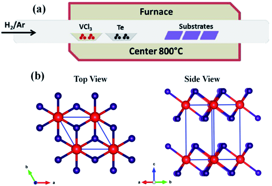 | ||
| Fig. 1 (a) Schematic of synthesis setup and (b) the crystal structure of 1T-VTe2. Red and violet balls are indicating vanadium(V), and tellurium (Te) atoms respectively. | ||
The morphology of CVD grown VTe2 crystals on mica and sapphire is shown in Fig. 2a–e. We were able to synthesize VTe2 single crystals on mica and sapphire substrates at the suitable growth parameters (see details in the Experimental section). It is noticeable that the hexagon is the dominant shape of VTe2 crystals (Fig. 2a and d) implying the single-crystalline nature of the samples. Atomic force microscopy (AFM) was used to measure the thickness of as-synthesized VTe2 crystal. Fig. 2c shows the thickness of VTe2 on the fluorphlogopite mica substrate was 90.5 nm. Energy-dispersive spectroscopy (EDS) was employed to identify the chemical composition of the synthesized VTe2 crystals on the sapphire substrate. Both V and Te elements are visualized by the EDS profile (Fig. 2f).
 | ||
| Fig. 2 (a) Optical microscopy (b) scanning electron microscopy (SEM) and (c) atomic force microscopy (AFM) images of as-synthesized VTe2 single crystals on fluorphlogopite mica substrates. (d and e) Optical and SEM images of the as-synthesized VTe2 single crystals on sapphire substrates respectively. (f) Elemental analysis of VTe2 crystal on sapphire substrate by energy-dispersive spectroscopy (EDS). | ||
Fig. 3 shows the X-ray photoelectron spectroscopy (XPS) spectra of 1T-VT2 single crystal grown on fluorphlogopite mica. The binding energies of V 2p3/2 and V 2p1/2 are 513.1 eV and 520.7 eV respectively are near to those in 1T-VS2 and 1T-VSe2![[thin space (1/6-em)]](https://www.rsc.org/images/entities/char_2009.gif) 31–34 and lower than that in VO2.35 The binding energies of Te 3d5/2 and Te 3d3/2 are 573.3 eV and 583.7 eV respectively comparable to the oxidation state of Te. In VTe2, the binding energy difference (ΔE) between V 2p3/2 and Te 3d5/2 is 60.2 eV, which is near to that of V and Te primary substance (60.7 eV), demonstrating that the V–Te bonds in VTe2 are weak because of the small electronegativity difference between V and Te.
31–34 and lower than that in VO2.35 The binding energies of Te 3d5/2 and Te 3d3/2 are 573.3 eV and 583.7 eV respectively comparable to the oxidation state of Te. In VTe2, the binding energy difference (ΔE) between V 2p3/2 and Te 3d5/2 is 60.2 eV, which is near to that of V and Te primary substance (60.7 eV), demonstrating that the V–Te bonds in VTe2 are weak because of the small electronegativity difference between V and Te.
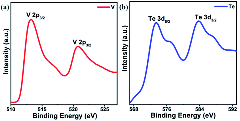 | ||
| Fig. 3 XPS spectra of 1T-VT2. (a) The V 2p3/2 and 2p1/2 peaks are seen to position at 513.1 eV and 520.7 eV respectively. (b) The Te 3d5/2 and 3d3/2 peaks are at 573.3 eV and 583.7 eV respectively. | ||
Moreover, we have investigated the growth of 2D VTe2 on h-BN/SiO2/Si substrate (Fig. 4a–c). It has been seen that large area VTe2 thin film (size ∼30–50 μm) with thickness ∼10.8 nm were grown on h-BN substrate applying the same growth condition used on sapphire and fluorphlogopite mica. Fig. 4d shows the room temperature Raman spectra of VTe2 film on the h-BN substrate at different laser intensities. At the laser intensity of 10 mW, three main peaks are observable at 92.6, 120.6, and 139.8 cm−1. The Raman spectrum of VTe2 crystal is consistent with the previous reports.26 According to earlier room temperature Raman measurements, the observable Raman peaks at 120.6 and 139.8 cm−1 are in plane Eg and out of plane A1g modes respectively.25,26 The weak Raman peak at 92.6 cm−1 could be related to the Eg phonons possibly coming from symmetry points.36,37
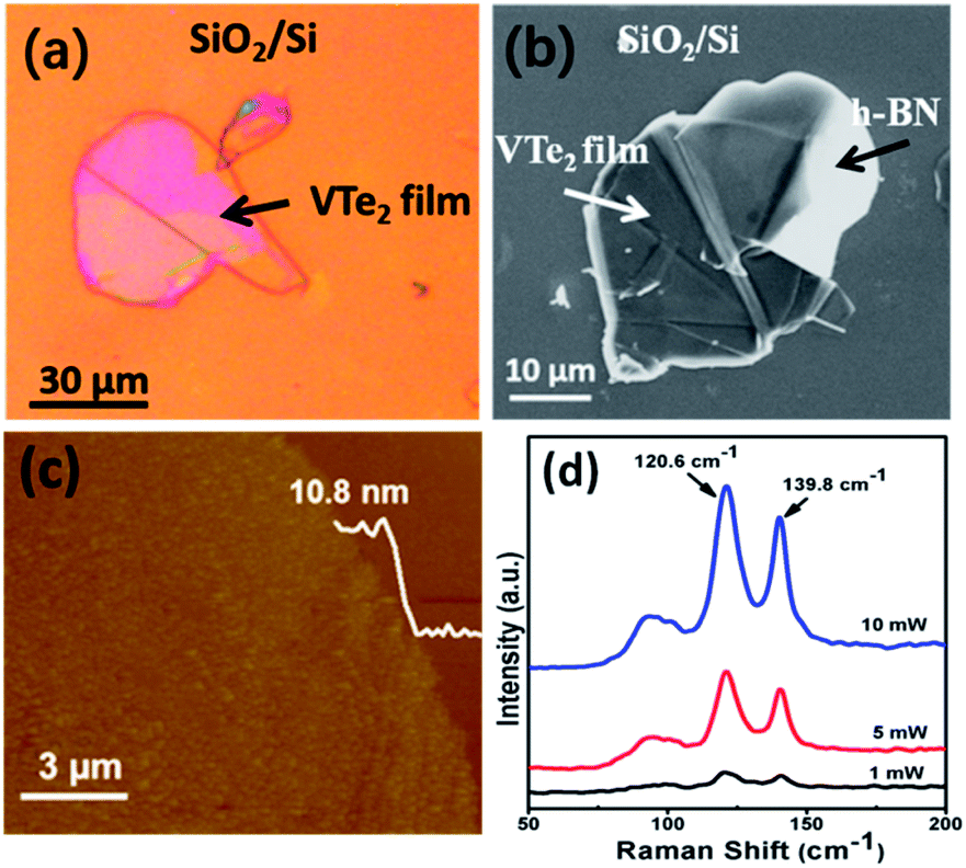 | ||
| Fig. 4 (a) Optical microscopy, (b) scanning electron microscopy (SEM), (c) atomic force microscopy (AFM) images and (d) room-temperature Raman spectra of as synthesized VTe2 thin film on the h-BN substrate. | ||
In recent years to explore the CDW phase transitions in TMDs, different research tools have been employed, such as scanning tunneling microscopy (STM),31,38–40 transmission electron microscopy (TEM),41,42 and angle-resolved photoemission spectroscopy (ARPES),31,40,43 and Raman spectroscopy. Raman spectroscopy is a non-destructive, high sensitive micro-area analysis method. It has been adopted as a very reliable technique to investigate the vibrational properties of 2D TMDs materials. Over the past few years, temperature-dependent Raman spectra of 1T-VS232 1T-VSe2,32,44–46 1T-TaS2,21 1T-TaSe2,47 2H-TaSe2,48,49 1T-TiSe2,50 and 2H-NbSe251 have been reported. Fig. 5a shows the temperature-dependent Raman spectra of VTe2 single crystal (thickness of ∼90 nm on sapphire) in the temperature range between 513 and 294 K. There are two Raman peaks observed at around 123.1, 142.9 cm−1 corresponding to the Eg and A1g vibration modes, respectively. It is noticeable that the overall Raman signal of VTe2 crystal is very weak from room temperature to 393 K, but become strong and sharp when the temperature reached at 413 K. This phenomenon was reproducible to several run and samples. The frequencies of the observed Raman modes are plotted as a function of temperature (Fig. 5b and c). The energy changes of the Raman modes 123.1, 142.9 cm−1 are more explicit with reducing the temperature. It has seen that the temperature dependence of these Raman modes' frequencies is almost the same and exhibits remarkable frequency changes at about 413 K, indicating that VTe2 undergoes a structural phase transition. This is also confirmed by the changes in the linewidth of 123.1, 142.9 cm−1 Raman modes. In Fig. 5d, the changes in the linewidth of these Raman modes are plotted as a function of temperature and shows a monotonous line expanding from the temperature at 413 K. This result is consistent with the observed CDW phase transition at 420 K by Won et al.30 but different from the observed structural phase transition at 474 K and 482 K.26,29 Table 1 summarizes the contrast of phase transition temperatures of VTe2 growth by different methods and characterized using different techniques.
 | ||
| Fig. 5 (a) Temperature-dependent Raman spectra of VTe2 single crystal at different temperature between 513 and 294 K. (b and c) Temperature dependent Raman shift of the Raman modes 123.1, 142.9 cm−1. (d) Changes in linewidth of the Raman modes 123.1, 142.9 cm−1 as a function of temperature. | ||
| Synthesis method | Characterization technique | Phase transition temperature | Reference |
|---|---|---|---|
| CVD | Raman spectroscopy | 413 K | This work |
| MBE | Raman spectroscopy and electrical measurements | 135 K and 240 K | 26 |
| CVT | Electrical and magnetic measurements | 473 K | 29 |
| Flux method | Electrical measurement | 420 K | 30 |
| CVT | Electrical and magnetic measurements | 475 K | 52 |
Furthermore, the electrical measurement was conducted for as-synthesized VTe2 single crystal (thickness ∼90 nm, sample length ≈13.63 μm, and width ≈6.14 μm) on a mica substrate. Fig. 6 shows a linear Ids–Vds curve with a resistance of ≈185 Ω and estimated conductivity is ≈1.3 × 10⁵ S m−1 at room temperature.
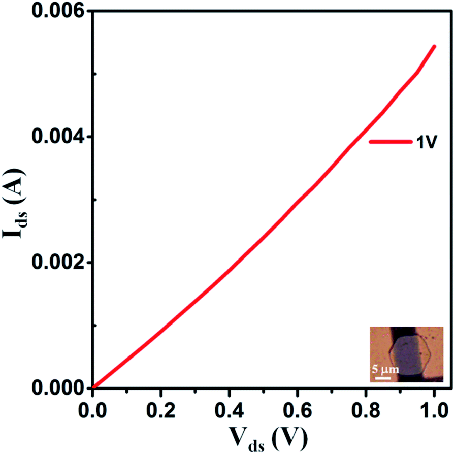 | ||
| Fig. 6 Current (Ids) versus source-drain voltage (Vds) of as synthesized VTe2 single crystal. Sample length ≈13.63 μm and width ≈6.14 μm. | ||
4. Conclusions
In conclusion, we have successfully synthesized 2D VTe2 single crystals on mica and sapphire substrates and large area VTe2 film on the h-BN substrate via the APCVD method. Temperature-dependent Raman shift, the linewidth of the 123.1, 142.9 cm−1 Raman modes of VTe2 crystal show the structural phase transition at around 413 K. Our investigation will provide the fundamental spectroscopy for 2D VTe2 crystal.Conflicts of interest
There are no conflicts to declare.Acknowledgements
L. X. acknowledges support from NSFC (21822502), the Key Research Program of Frontier Sciences of CAS (QYZDB-SSW-SYS031) and the Strategic Priority Research Program of CAS (XDB30000000).References
- J. Wilson, F. Di Salvo and S. Mahajan, Adv. Phys., 1975, 24, 117 CrossRef CAS
.
- T. Straub, T. Finteis, R. Claessen, P. Steiner, S. Hüfner, P. Blaha, C. S. Oglesby and E. Bucher, Phys. Rev. Lett., 1999, 82, 4504 CrossRef CAS
- F. Weber, S. Rosenkranz, J. P. Castellan, R. Osborn, R. Hott, R. Heid, K. P. Bohnen, T. Egami, A. H. Said and D. Reznik, Phys. Rev. Lett., 2011, 107, 107403 CrossRef CAS
- M. Eichberger, H. Schafer, M. Krumova, M. Beyer, J. Demsar, H. Berger, G. Moriena, G. Sciaini and R. J. D. Miller, Nature, 2010, 468, 799 CrossRef CAS
- C. Dang, M. Guan, S. Hussain, W. Wen, Y. Zhu, L. Jiao, S. Meng and L. Xie, Nano Lett., 2020, 20(9), 6725–6731 CrossRef CAS
- W. Wen, C. Dang and L. Xie, Chinese Phys. B, 2019, 28(5), 058504 CrossRef CAS
- W. Wen, Y. Zhu, C. Dang, W. Chen and L. Xie, Nano Lett., 2019, 19(2), 1805–1813 CrossRef CAS
- T. Yokoya, T. Kiss, A. Chainani, S. Shin, M. Nohara and H. Takagi, Science, 2001, 294, 2518–2520 CrossRef CAS
- B. Sipos, A. F. Kusmartseva, A. Akrap, H. Berger, L. Forro and E. Tutis, Nat. Mater., 2008, 7, 960 CrossRef CAS
- R. Ang, Y. Tanaka, E. Ieki, K. Nakayama, T. Sato, L. J. Li, W. J. Lu, Y. P. Sun and T. Takahashi, Phys. Rev. Lett., 2012, 109, 176403 CrossRef CAS
- K. Xu, P. Chen, X. Li, C. Wu, Y. Guo, J. Zhao, X. Wu and Y. Xie, Angew. Chem., Int. Ed., 2013, 52, 10477 CrossRef CAS
- X. Zhu, Y. Guo, H. Cheng, J. Dai, X. An, J. Zhao, K. Tian, S. Wei, X. C. Zeng, C. Wu and Y. Xie, Nat. Commun., 2016, 7, 11210 CrossRef CAS
- H. L. Zhuang and R. G. Hennig, Phys. Rev. B: Condens. Matter Mater. Phys., 2016, 93, 054429 CrossRef
- M. Dressel, Naturwissenschaften, 2007, 94, 527 CrossRef CAS
- P. Monceau, in Physics and Chemistry of Low-Dimensional Inorganic Conductors, ed. C. Schlenker, J. Dumas, M. Greenblatt and S. van Smaalen, Plenum Press Div Plenum Publishing Corp, New York, 1996, vol. 354, p. 371 Search PubMed
- K. Rossnagel, J. Phys.: Condens. Matter, 2011, 23, 213001 CrossRef CAS
- J. A. Wilson, F. J. Di Salvo and S. Mahajan, Adv. Phys., 2001, 50, 1171 CrossRef
- A. M. Gabovich, A. I. Voitenko and M. Ausloos, Phys. Rep., 2002, 367, 583 CrossRef CAS
- G. Liu, B. Debnath, T. R. Pope, T. T. Salguero, R. K. Lake and A. A. Balandin, Nat. Nanotechnol., 2016, 11, 845–850 CrossRef CAS
- I. Vaskivskyi, I. A. Mihailovic, S. Brazovskii, J. Gospodaric, T. Mertelj, D. Svetin, P. Sutar and D. Mihailovic, Nat. Commun., 2016, 7, 11442 CrossRef CAS
- X. Wang, H. Liu, J. Wu, J. Lin, W. He, H. Wang, X. Shi, K. Suenaga and L. Xie, Adv. Mater., 2018, 30, 1800074 CrossRef
- M. Chhowalla, H. S. Shin, G. Eda, L.-J. Li, K. P. Loh and H. Zhang, Nat. Chem., 2013, 5, 263 CrossRef
- Y. Ma, Y. Dai, M. Guo, C. Niu, Y. Zhu and B. Huang, ACS Nano, 2012, 6, 1695 CrossRef CAS
- K. Xu, P. Chen, X. Li, C. Wu, Y. Guo, J. Zhao, X. Wu and Y. Xie, Angew. Chem., Int. Ed., 2013, 52, 10477 CrossRef CAS
- J. Li, B. Zhao, P. Chen, R. Wu, B. Li, Q. Xia, G. Guo, J. Luo, K. Zang, Z. Zhang, H. Ma, G. Sun, X. Duan and X. Duan, Adv. Mater., 2018, 30, 1801043 CrossRef
- X. Ma, T. Dai, S. Dang, S. Kang, X. Chen, W. Zhou, G. Wang, H. Li, P. Hu, Z. He, Y. Sun, D. Li, F. Yu, X. Zhou, H. Chen, X. Chen, S. Wu and S. Li, ACS Appl. Mater. Interfaces, 2019, 11, 10729 CrossRef CAS
- K. Bronsema, G. Bus and G. Wiegers, J. Solid State Chem., 1984, 53, 415 CrossRef CAS
- A. Nakamura, T. Shimojima, M. Matsuura, Y. Chiashi, M. Kamitani, H. Sakai, S. Ishiwata, H. Li, A. Oshiyama and K. Ishizaka, Appl. Phys. Express, 2018, 11, 092601 CrossRef
- T. Ohtani, S. Onoue and M. Nakahira, Mater. Res. Bull., 1984, 19, 1367–1375 CrossRef CAS
- http://meetings.aps.org/link/BAPS.2018.MAR.C18.5.
- M. Bonilla, S. Kolekar, Y. Ma, H. C. Diaz, V. Kalappattil, R. Das, T. Eggers, H. R. Gutierrez, M. H. Phan and M. Batzill, Nat. Nanotechnol., 2018, 13, 289–293 CrossRef CAS
- M. Hossain, J. Wu, W. Wen, H. Liu, X. Wang and L. Xie, Adv. Mater. Interfaces, 2018, 1800528 CrossRef
- X. Chia, A. Ambrosi, P. Lazar, Z. Sofer and M. Pumera, J. Mater. Chem. A, 2016, 4, 14241–14253 RSC
- J. Zhang, C. Zhang, Z. Wang, J. Zhu, Z. Wen, X. Zhao, X. Zhang, J. Xu and Z. Lu, Small, 2018, 14, 1703098 CrossRef
- D. Malarde, I. D. Johnson, I. J. Godfrey, M. J. Powell, G. Cibin, R. Quesada-Cabrera, J. A. Darr, C. J. Carmalt, G. Sankar, I. P. Parkin and R. G. Palgrave, J. Mater. Chem. C, 2018, 6, 11731–11739 RSC
- R. Samnakay, D. Wickramaratne, T. R. Pope, R. K. Lake, T. T. Salguero and A. A. Balandin, Nano Lett., 2015, 15, 2965–2973 CrossRef CAS
- H. Wang, Y. Chen, M. Duchamp, Q. Zeng, X. Wang, S. H. Tsang, H. Li, L. Jing, T. Yu, E. H. T. Teo and Z. Liu, Adv. Mater., 2018, 30, 1704382 CrossRef
- C. J. Arguello, E. P. Rosenthal, E. F. Andrade, W. Jin, P. C. Yeh, N. Zaki, S. Jia, R. J. Cava, R. M. Fernandes, A. J. Millis, T. Valla, R. M. Osgood and A. N. Pasupathy, Phys. Rev. Lett., 2015, 114, 037001 CrossRef CAS
- J. Feng, A. Tan, S. Wagner, J. Liu, Z. Mao, X. Ke and P. Zhang, Appl. Phys. Lett., 2016, 109, 021901 CrossRef
- H. Ryu, Y. Chen, H. Kim, H. Z. Tsai, S. Tang, J. Jiang, F. Liou, S. Kahn, C. Jia, A. A. Omrani, J. H. Shim, Z. Hussain, Z. X. Shen, K. Kim, B. I. Min, C. Hwang, M. F. Crommie and S. K. Mo, Nano Lett., 2018, 18, 689–694 CrossRef CAS
- J. Shi, X. Chen, L. Zhao, Y. Gong, M. Hong, Y. Huan, Z. Zhang, P. Yang, Y. Li, Q. Zhang, Q. Zhang, L. Gu, H. Chen, J. Wang, S. Deng, N. Xu and Y. Zhang, Adv. Mater., 2018, 1804616 CrossRef
- W. T. Adam, R. Hovden, D. Wang, Y. D. Kim, J. Okamoto, K. A. Spoth, Y. Liu, W. Lu, Y. Sun, J. C. Hone, L. F. Kourkoutis, P. Kim and A. N. Pasupathy, Proc. Natl. Acad. Sci. U. S. A., 2015, 112, 15054 CrossRef
- L. Bawden, S. P. Cooil, F. Mazzola, J. M. Riley, L. J. Collins-McIntyre, V. Sunko, K. W. B. Hunvik, M. Leandersson, C. M. Polley, T. Balasubramanian, T. K. Kim, M. Hoesch, J. W. Wells, G. Balakrishnan, M. S. Bahramy and P. D. C. King, Nat. Commun., 2016, 7, 11711 CrossRef CAS
- M. Hossain, Z. Zhao, W. Wen, X. Wang, J. Wu and L. Xie, Crystals, 2017, 7, 298 CrossRef
- B. Dardel, M. Grioni, D. Malterre, P. Weibel, Y. Baer and F. Levy, J. Phys.: Condens. Matter, 1993, 5, 6111–6120 CrossRef CAS
- M. M. Ugeda, A. J. Bradley, Y. Zhang, S. Onishi, Y. Chen, W. Ruan, C. O. Aristizaba, H. Ryu, T. Mark, M. T. Edmonds, H. Z. Tsai, A. Riss, S. K. Mo, D. Lee, A. Zettl, Z. Hussain, Z. X. Shen and M. F. Crommie, Nat. Phys., 2016, 12, 92–97 Search PubMed
- H. X. Luo, W. W. Xie, J. Tao, H. Inoue, A. Gyenis, J. W. Krizan, A. Yazdani, Y. M. Zhu and R. J. Cava, Proc. Natl. Acad. Sci. U. S. A., 2015, 112, E1174–E1180 CrossRef CAS
- E. Morosan, H. W. Zandbergen, B. S. Dennis, J. W. G. Bos, Y. Onose, T. Klimczuk, A. P. Ramirez, N. P. Ong and R. J. Cava, Nat. Phys., 2006, 2, 544 Search PubMed
- T. Shimada, F. S. Ohuchi and A. Koma, Surf. Sci., 1993, 291, 57–66 CrossRef CAS
- P. Goli, J. Khan, D. Wickramaratne, R. K. Lake and A. A. Balandin, Nano Lett., 2012, 12, 5941–5945 CrossRef CAS
- X. Xi, L. Zhao, Z. Wang, H. Berger, L. Forró, J. Shan and K. F. Mak, Nat. Nanotechnol., 2015, 10, 765–769 CrossRef CAS
- T. Ohtani, K. Hayashi, M. Nakahira and H. Nozaki, Solid State Commun., 1981, 40, 629–631 CrossRef CAS
| This journal is © The Royal Society of Chemistry 2021 |