
 Open Access Article
 This Open Access Article is licensed under a Creative Commons Attribution-Non Commercial 3.0 Unported Licence
Effect of annealing on the defect-mediated blue phosphorescence in ZnO nanocrystals†
Sagnik Dasa,
Uttam Kumar Ghoraib,
Rajib Deyc,
Chandan Kumar Ghosh c and
Mrinal Pal*a
c and
Mrinal Pal*a
aCSIR-Central Glass and Ceramic Research Institute, Kolkata-700032, India. E-mail: palm@cgcri.res.in
bRamakrishna Mission Vidyamandira, Howrah-711202, India
cJadavpur University, Kolkata-700032, India
First published on 23rd December 2020
Abstract
Recently, UV/NUV excitable RGB phosphors with precisely tunable PL emission properties have been in high demand for their suitability in the fabrication of white LEDs. In this paper, we report to have tuned the PL intensity, shade, and color temperature of the defect-mediated blue phosphorescence of ZnO nanopowders by systematic annealing at different temperatures. The ZnO nanopowder was prepared by a facile and cost-effective aqueous solution-precipitation method. The as-synthesized nanopowder was annealed at different temperatures ranging from 150 °C to 850 °C and all these samples were characterized by XRD, FESEM, EDX, BET, Raman spectroscopy, and UV-Vis spectroscopy to have insight into their microstructural, compositional, and band-structure details. Optical studies of the samples were conducted by PL and τ-PL spectroscopy. Color coordinates of the samples were obtained from the CIE plots derived from the PL spectra. The CIE coordinates were further used to calculate the CCT values of the samples. τ-PL spectroscopy was carried out to measure the life-time of the photogenerated electrons. PL studies of the samples revealed that the blue emissions have red, yellow, and blue components originating from crystalline point defects, viz. zinc interstitial (Zni), and oxygen interstitial (Oi). Annealing at different temperatures triggered changes in the defect concentrations leading to the corresponding changes in the intensity, shade, and color temperature of the blue phosphorescence.
Introduction
Phosphors are an important class of semiconductor and find applications in field emission displays (FED), flat panel displays, vacuum fluorescent displays (VFD), plasma display panels (PDP)1–5 etc. Recently, the most sought-after thing in the lighting industry has been white LEDs (W-LEDs). The commercial technique of producing W-LEDs is to combine blue LEDs (indium gallium nitride) with a yellow phosphor (Ce3+ doped yttrium aluminium garnate).6 However, this technique suffers from poor colour rendition, high CCT (>7000 K), and harmful effects of blue LEDs on the human eye and body.7–10 By far the best method for producing W-LEDs has been a combination of an ultraviolet/near ultraviolet (UV/NUV) LED with RGB phosphors.11–14 However, true whiteness in emission is achieved only when red, green, and blue colours are combined in correct proportions. This necessitates the development of phosphors with precise tunability in emission.ZnO is an important optoelectronic material having a direct and wide (3.3 eV) band gap and large exciton binding energy (60 meV).15–17 Consequently, ZnO exhibits phosphorescence originating from crystalline point defects, viz. oxygen vacancy, zinc vacancy, oxygen interstitial, zinc interstitial etc.18–24 Different approaches have been adopted in order to tune such defect-mediated phosphorescence by controlling the type and concentration of the crystalline defects. Recently, Rauwel et al. has reported on the precursor dependance of the defect mediated (oxygen vacancy and zinc interstitial/vacancy) blue-green PL emission in ZnO nanoparticles.25 This study suggests that the type and concentration of the point defects in ZnO can be potentially tailored by the choice of appropriate precursors, thereby tuning the PL color and intensity. PL properties of ZnO can also be tuned by changing morphologies of the nanoparticles. For example, Gong et al. reported enhancement of PL emission in ZnO nanoparticles with rose-like morphology.26 Singh et al. observed a quenching of PL emission with increasing rGO concentration in graphene–ZnO hybrid nanostructure.27 Djurišić et al. and Zhang et al. reported that PL emission in ZnO can be manipulated by varying the excitation wavelength.28,29 Very recently, Garcia et al. reported that defect-mediated white phosphorescence in ZnGa2O4 can be controlled by modifying the annealing atmosphere.30 In principle, it is possible to tune the defect concentration and hence the intensity, color/shade, and color temperature of phosphorescence in ZnO also by varying annealing temperature. However, any such systematic study can hardly be found in the prior art.
In this paper we have reported monotonic changes in the PL properties, viz. intensity, shade, life-time etc. of the defect-mediated blue phosphorescence in ZnO nanopowder by systematic annealing at different temperatures. ZnO nanopowder was prepared by a facile, and cost-effective solution-precipitation method. The as prepared nanopowder was annealed at seven different temperatures ranging from 150 °C to 850 °C in ordinary atmosphere. The nanopowders annealed at different temperatures were characterized by XRD (X-ray diffraction), FESEM (field emission scanning electron microscopy), EDX (Energy Dispersive X-ray), BET (Brunauer–Emmett–Teller), and micro-Raman spectroscopy to have an insight into the microstructure of the material. The photoluminescence emission spectra of all the samples revealed that the blue emissions were comprised of red, yellow, and blue components originating from crystalline point defects, viz. zinc interstitial (Zni), and oxygen interstitial (Oi). Plausible reaction mechanisms explaining their origins have been proposed. The concentrations of these defects and the intensities of the corresponding PL emission peaks varied as a function of annealing temperature. The corresponding CIE plots revealed that the shade of the emission gradually turned from light blue (CIE co-ordinate: (0.33, 0.30)) to dark blue (CIE co-ordinate: (0.27, 0.26)) as the annealing temperature increased from 150 °C to 850 °C. A thermodynamic interpretation to such variance in defect concentrations has been proposed. τ-PL study and correlated color temperature (CCT) calculations revealed phosphorescence and cool lighting in all the samples. Finally, all the samples exhibited quantum yields comparable to other ZnO based materials. This study suggests that this ZnO based blue phosphor owing to its tunable phosphorescence can be readily used for white LED fabrication. Further this study establishes thermal annealing as a technique for tuning of defect-mediated phosphorescence.
Experimental
Materials
Zinc nitrate hexahydrate (Zn(NO3)2·6H2O) (reagent grade, 98%, MW = 189.36 g mol−1) and ammonium hydroxide (25% ammonia solution) were procured from Sigma-Aldrich and E-merck, respectively. DI water was prepared in house.Methods
ZnO nanoparticles were synthesized by a simple aqueous solution-precipitation route under ordinary atmosphere. 2.97 g of zinc nitrate hexahydrate (Merck) was dissolved in 100 ml of DI water and the solution was heated to 100 °C. To this solution 20 c.c. ammonium hydroxide (25% ammonia solution, Merck) was added dropwise until a pH of 10 was achieved. Thereafter, the solution was refluxed at 100 °C for 1 h in a flat bottom flask under continuous stirring at 1000 rpm. After 1 h, a dense white solid was precipitated. The precipitate was collected by centrifugation at 10![[thin space (1/6-em)]](https://www.rsc.org/images/entities/char_2009.gif) 000 rpm for 10 minutes and dried at 80 °C for 5 h in ordinary atmosphere. This sample was annealed at different temperatures viz. 150 °C, 350 °C, 450 °C, 550 °C, 650 °C, 750 °C, and 850 °C under ordinary atmosphere for 3 h each. The annealed samples were designated as BZ150, BZ350, BZ450, BZ550, BZ650, BZ750, and BZ850, where BZ stands for ‘Base ZnO’ sample and the numerical values represent the annealing temperatures of the respective samples. Fig. 1 schematically illustrates the synthesis process. Additionally, BZ550-Ar and BZ550-O2 samples were prepared by annealing the dried precipitate at 550 °C for 3 h in argon atmosphere and oxygen atmosphere, respectively.
000 rpm for 10 minutes and dried at 80 °C for 5 h in ordinary atmosphere. This sample was annealed at different temperatures viz. 150 °C, 350 °C, 450 °C, 550 °C, 650 °C, 750 °C, and 850 °C under ordinary atmosphere for 3 h each. The annealed samples were designated as BZ150, BZ350, BZ450, BZ550, BZ650, BZ750, and BZ850, where BZ stands for ‘Base ZnO’ sample and the numerical values represent the annealing temperatures of the respective samples. Fig. 1 schematically illustrates the synthesis process. Additionally, BZ550-Ar and BZ550-O2 samples were prepared by annealing the dried precipitate at 550 °C for 3 h in argon atmosphere and oxygen atmosphere, respectively.
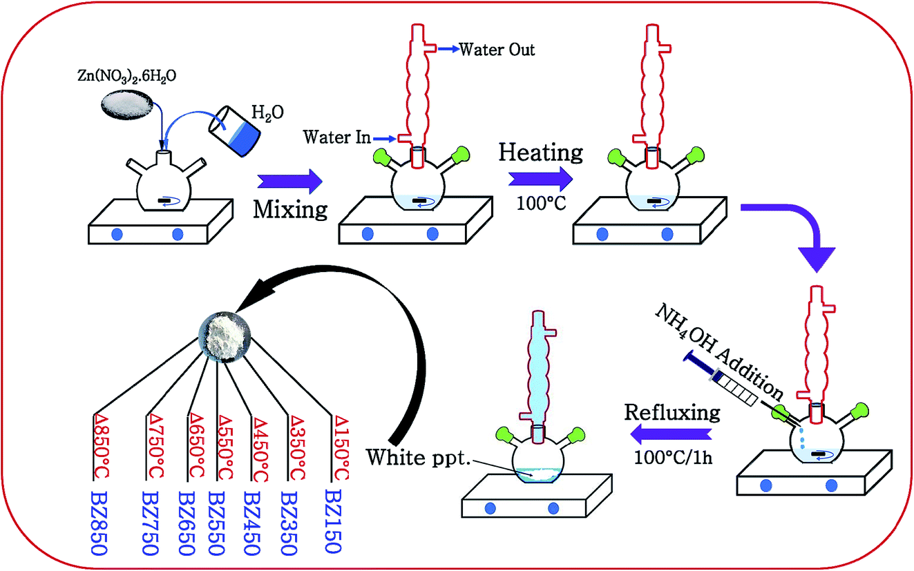 | ||
| Fig. 1 Schematic illustration of the synthesis of BZ150, BZ350, BZ450, BZ550, BZ650, BZ750, and BZ850 samples. | ||
Characterization
X-ray diffraction (XRD) patterns were recorded by Ultima III diffractometer (Cu Kα radiation, λ = 1.5404 Å, Rigaku, Japan) to identify the phases present in the samples. Particle morphologies and elemental compositions of the samples were studied by field emission scanning electron microscopy and EDX study, respectively (FESEM, Hitachi S-4800). The specific surface area of the nanopowders were determined by BET study ((NovaWin, Quantachrome Instruments). For the FESEM analysis, samples were dispersed in isopropanol using an ultrasonic bath (250 W, Rivotek) and drop coated on hard aluminium foils. Room temperature micro-Raman spectroscopy of the samples was done using an alpha 300, WITEC, Germany having a laser source at 532 nm. Photoluminescence spectra were recorded at room temperature by using a spectrofluorometer (Edinburgh FLSP-980), having a Xe lamp source with an excitation wavelength of 300 nm to study the defect induced emission and their systematic variation in intensity with annealing temperature as the parameter. An Aquarius 7200 UV-Vis spectrometer was used to carry out the optical absorption study at room temperature. The Commission Internationale de I'Eclairage (CIE) coordinates were calculated for the emission spectrum which is the superimposition of different emission spectra weighted to their concentrations. Lifetime of the photogenerated electrons for all the samples were investigated by an Edinburgh FLSP-980 make time resolved PL spectroscope.Results and discussion
Structural characterization
The XRD patterns of BZ150, BZ350, BZ450, BZ550, BZ650, BZ750, and BZ850 samples are shown in Fig. 2A. Several diffraction peaks at different positions are detectable from all the patterns. The crystallographic planes corresponding to these peaks have been marked on the diffraction pattern of BZ150 and shown in Fig. 2B. All the peak positions match well with the wurtzite ZnO (JCPDS card no. 36-1451).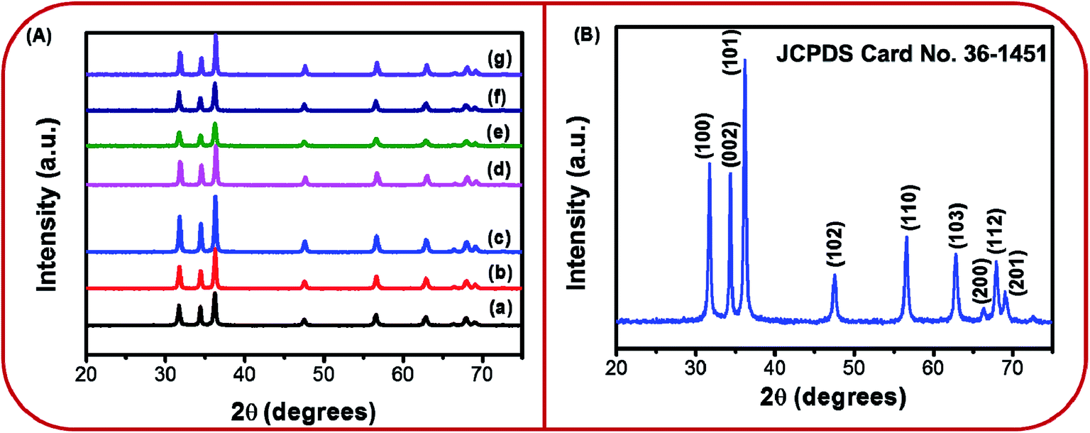 | ||
| Fig. 2 (A) XRD patterns of (a) BZ150, (b) BZ350, (c) BZ450, (d) BZ550, (e) BZ650, (f) BZ750, (g) BZ850, and (B) XRD pattern of BZ150 with detectable crystallographic planes marked on it. | ||
No extra peak suggestive of any impurity is there. Sharp peaks observed in the XRD pattern indicate highly crystalline nature of prepared ZnO nanopowder. The average crystallite sizes of BZ150, BZ350, BZ450, BZ550, BZ650, BZ750, and BZ850 samples as calculated from the Scherrer equation are found to be 27 nm, 29 nm, 32 nm, 31 nm, 25 nm, 28 nm, and 34 nm, respectively.
Fig. 3 shows the typical FESEM images of all the samples. From the images it is clear that the particles are agglomerated to some extent. In spite of agglomeration cauliflower like morphology is visible in the FESEM images of the BZ150, BZ350, BZ450, BZ550, BZ650 and BZ750 samples. However, BZ850 sample shows spherical to extended spherical morphologies. Also, the particle sizes of BZ150, BZ350, BZ450 and BZ550 samples are in the range of 50–500 nm i.e. a wide variation of particle size can be observed. However, in BZ650, BZ750, and BZ850 samples comprise of mostly large (∼500 nm) particles and small particles have almost disappeared. This indicates that at temperatures higher than 550 °C Ostwald ripening starts eliminating the smaller particles and above 750 °C sintering starts changing the cauliflower like particles into spherical ones.
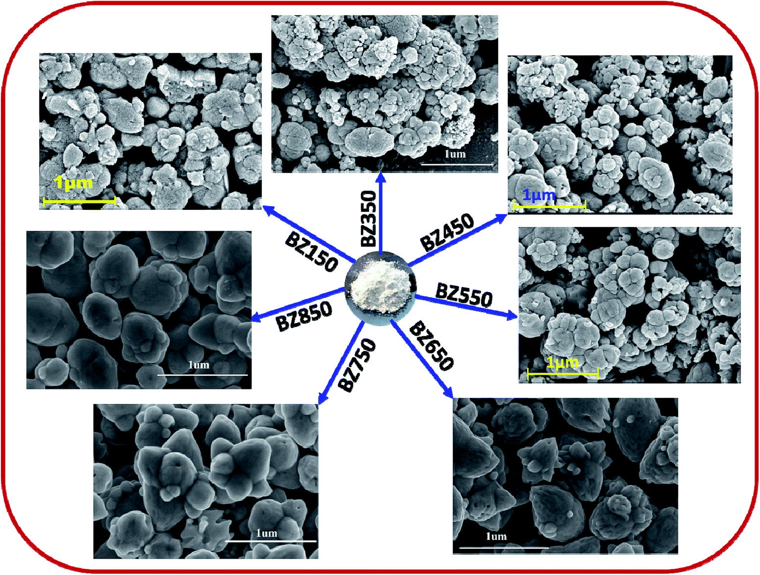 | ||
| Fig. 3 FESEM images of BZ150, BZ350, BZ450, BZ550, BZ650, BZ750, and BZ850 samples. | ||
Zn-to-O ratio for three representative samples, viz. BZ150, BZ550, and BZ850 have been determined by EDX study (ref. ESI-Fig. I† for EDX spectrums) and listed in Table 1. The Zn-to-O ratio increases from ∼0.59 in BZ150 to ∼0.85 in BZ850. The Zn to O ratio is less than one in each case. This clearly suggests the presence of oxygen interstitial (Oi) defects in all the samples. Further, this is also suggestive of the gradual annihilation of the oxygen interstitial (Oi) defects with increase in annealing temperature, especially at higher temperatures.
| Sample | Zn (atomic%) | O (atomic%) | Zn/O atomic ratio |
|---|---|---|---|
| BZ150 | 37.18 | 62.82 | 0.59 |
| BZ550-Ar | 41.38 | 58.62 | 0.70 |
| BZ550 | 40.16 | 59.84 | 0.67 |
| BZ550-O2 | 37.43 | 62.57 | 0.59 |
| BZ850 | 46.13 | 53.87 | 0.85 |
It was further observed that the Zn-to-O ratio in BZ550-Ar, BZ550, and BZ550-O2 are ∼0.70, ∼0.67, and ∼0.59, respectively (ref. Table 1). It is expected that with the increase in oxygen partial pressure in the annealing atmosphere, the removal of oxygen interstitial defect would reduce and this has been reflected in the reduction of Zn to O ratio with increasing oxygen partial pressure in the annealing atmosphere. No extra peak for any impurity element in the samples is observed in the EDX spectra (Au peaks are present as gold was sputtered on the samples for conducting FESEM and EDX studies) and this is in agreement with the XRD spectra of the samples (ref. Fig. 2) showing no peaks other than wurtzite ZnO.
It is observed from FESEM study that the particle sizes are in the range of 50–500 nm. However, the crystallite sizes as calculated from the Scherrer equation are less than 34 nm. We need to resolve this apparent inconsistency. FESEM provides particle size. However, from Scherrer equation we get crystallite size. A crystallite is essentially a single crystal. Visible particles are seldom comprised of single crystallites except for some materials such as Si, Ge, some Ni based super-alloys etc. Generally, we deal with polycrystalline particles whereby a single particle is comprised of multiple crystallites, also known as grains in case of powder materials. Therefore, the particle size of a polycrystalline material would be bigger than the crystallite size. The presence of multiple peaks in the X-ray diffraction patterns of the samples reported in this work clearly suggests that all these samples are polycrystalline. Therefore, the particle sizes observed in FESEM images are much larger than the crystallite sizes calculated by Scherrer equation. However, with increasing crystallite size particle size definitely increases. The crystallite sizes of the samples increase from BZ150 to BZ850 and this suggests that particle size should also follow the same trend.
The coarsening of the nanoparticles with increasing annealing temperature was revealed by the BET study of BZ150, BZ550, and BZ850 (ref. ESI-Fig. II†). The specific surface areas of BZ150, BZ550, and BZ850 as derived from BET study are listed in Table 2.
| Sample | Specific surface area (m2 g−1) |
|---|---|
| BZ150 | 6.793 |
| BZ550 | 5.743 |
| BZ850 | 1.858 |
BET specific surface area decreases marginally from BZ150 to BZ550. However, the BET specific surface area of BZ850 sample is considerably lower than that of BZ150 or BZ550 sample. This clearly suggests the onset of coarsening at higher temperatures. This result is also corroborated by FESEM images.
Fig. 4A(a)–(g) show the Raman spectra of all the samples in the wavenumber range of 0–3000 cm−1. Group theory predicts that the Raman active zone-center optical phonons are A1 + 2E2 + E1 + 2B1. It is known that the B1 mode is silent. The E1 and A1 modes are polar. They exhibit different frequencies for the transverse-optical (TO) and longitudinal-optical (LO) phonon modes. E1 and A1 are Raman active modes. The non-polar E2 modes are Raman active and show two different frequencies viz. E2 (high) and E2 (low).31,32
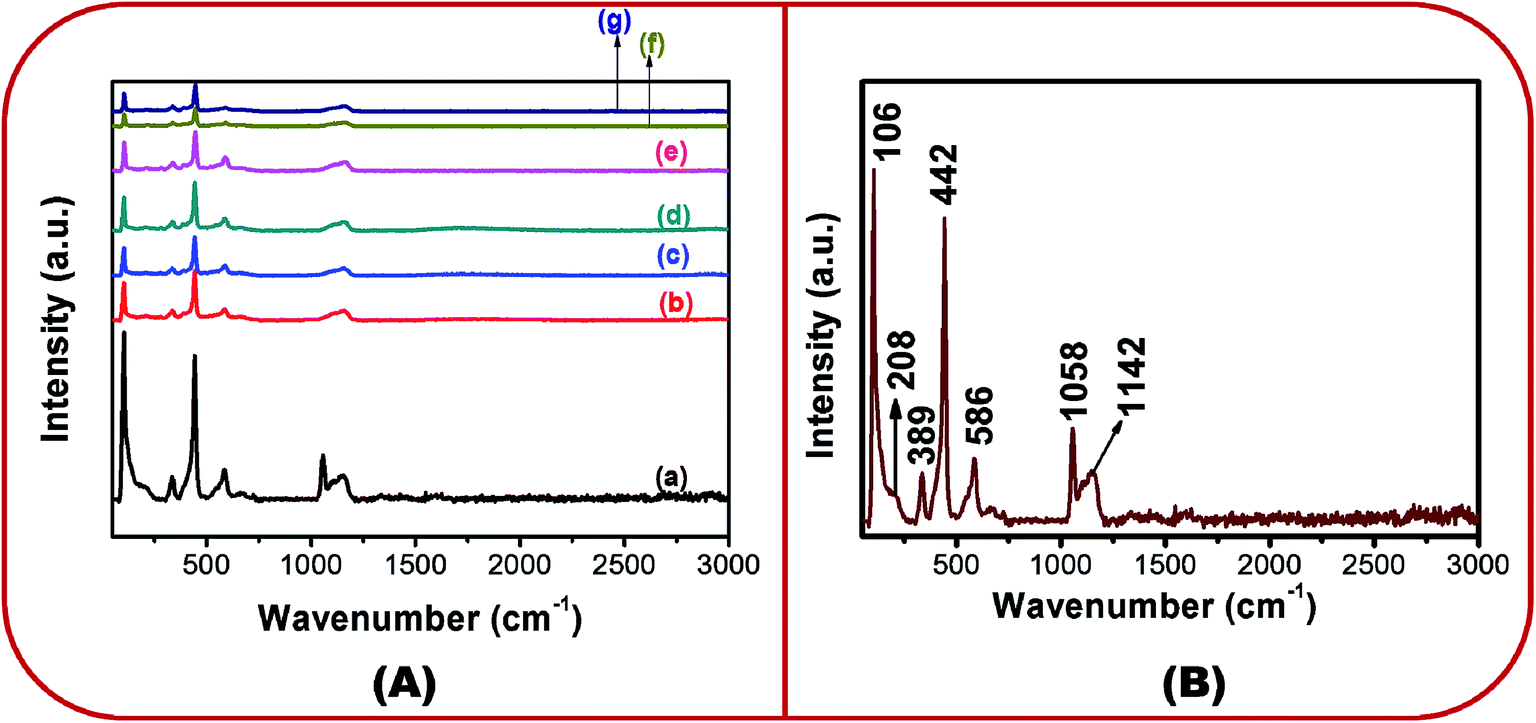 | ||
| Fig. 4 (A) Micro-Raman spectra of (a) BZ150, (b) BZ350, (c) BZ450, (d) BZ550, (e) BZ650, (f) BZ750 and (g) BZ850 samples, and (B) marked micro-Raman spectra of BZ150. | ||
In Fig. 4A, for all the samples several peaks are visible. These peaks have been marked in the micro Raman spectra of BZ150 for facile understanding (ref. Fig. 4B). The exact peak positions are listed in ESI-Table 1.† The first five peaks (ref. Fig. 4B) can be ascribed to the E2 (low), 2E2 (low), A1 (TO), E2 (high), and E1 (LO) modes, respectively.33,34 The peak at 1046 cm−1 could not be explained and the peak at ∼1150 cm−1 is ascribed to the E2 (LO) mode.35
The peak at 104 cm−1 is due to the Zn ions.33 The peak at 442 cm−1 is the band characteristic of wurtzite ZnO. Here, blue shifts of 3 cm−1, 3 cm−1, 5 cm−1, 6 cm−1, 5 cm−1, 5 cm−1, and 6 cm−1 have been observed with respect to the standard position of this peak (439 cm−1) in BZ150, BZ350, BZ450, BZ550, BZ650, BZ750, and BZ850 samples, respectively. This may be attributed to the oxygen excess defects in the lattice.35 A plausible mechanism has been proposed in a latter section in order to explain the inclusion of such oxygen excess defects.
The A1 (TO) mode is related to the crystallinity of ZnO.36 Strong blue shiftings (19 cm−1, 17 cm−1, 20 cm−1, 17 cm−1, 22 cm−1, 17 cm−1, and 24 cm−1 in BZ150, BZ350, BZ450, BZ550, BZ650, BZ750, and BZ850 samples, respectively) of the peak with respect to its standard position have been observed. Such significant blue shiftings in the peak position are suggestive of considerable anisotropy in the crystal structure of the samples. Such anisotropy might have originated from the oriented growth of the ZnO samples as shown in FESEM study (ref. Fig. 3). The peaks lying between 570–590 cm−1 are related to oxygen vacancy (VO) and/or Zni defects.37,38 The possibility of the generation of VO may be discarded owing to the use of oxygen rich precursor salt. Therefore, the peaks at ∼584 cm−1 may be ascribed to Zni defects.
Also, the 442 cm−1 peaks representing the Oi defects are far more intense than the respective ∼584 cm−1 peaks representing the Zni defects for all the samples. Thus, it is expected that the concentration of the Oi defects would be more than that of the Zni defects for all the samples. This has been further corroborated by the EDX study which clearly shows that the Zn/O ratio is less than 1 for all the samples (ref. ESI-Fig. I and Table 1†). The peak at ∼1150 cm−1 corresponds to the cationic and anionic defects.
Study of optical properties by photoluminescence (PL) and time resolved PL (τ-PL) spectroscopy
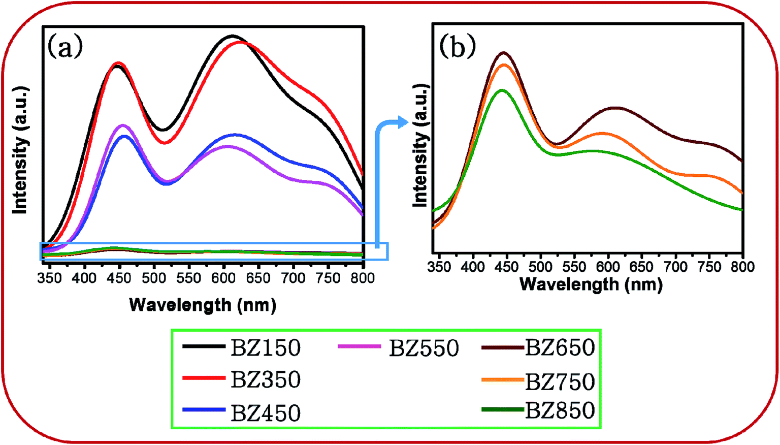 | ||
| Fig. 5 (a) PL spectra of BZ150, BZ350, BZ450, BZ550, BZ650, BZ750 and BZ850 samples, and (b) zoomed PL spectra of BZ650, BZ750 and BZ850 samples. | ||
Conventionally, PL spectra of ZnO show one peak in the UV region at ∼355 nm corresponding to the band to band transition.39 However, the peaks in the UV region corresponding to band to band and band edge transitions are absent for all the samples. It seems plausible that the tail of the high intensity visible emissions near the band edge has masked such emissions in the UV region. Since the intensities of the emissions in the UV region are inconsequential with respect to that of the visible emissions, these emissions will not be considered for further discussion.
However, band gap energy is essential information in explaining the origin of the visible emissions. UV-Vis analysis was conducted in order to get this information. Fig. 6 shows the UV-Vis plot for BZ150 sample. Two different energies, viz. 3.3 eV and 3.5 eV that are obtained from this plot can be attributed to excitonic transition40 and band to band transition.39 From these energy values the peak positions for excitonic and band to band transition are calculated as 375 nm and 355 nm, respectively. However, these peaks are not visible in the PL spectrum as mentioned earlier. Since the particle size of all the samples are much bigger than the Debye length for ZnO, it may be expected that the band gap of all the samples will be similar to that of BZ150, viz. ∼3.5 eV.
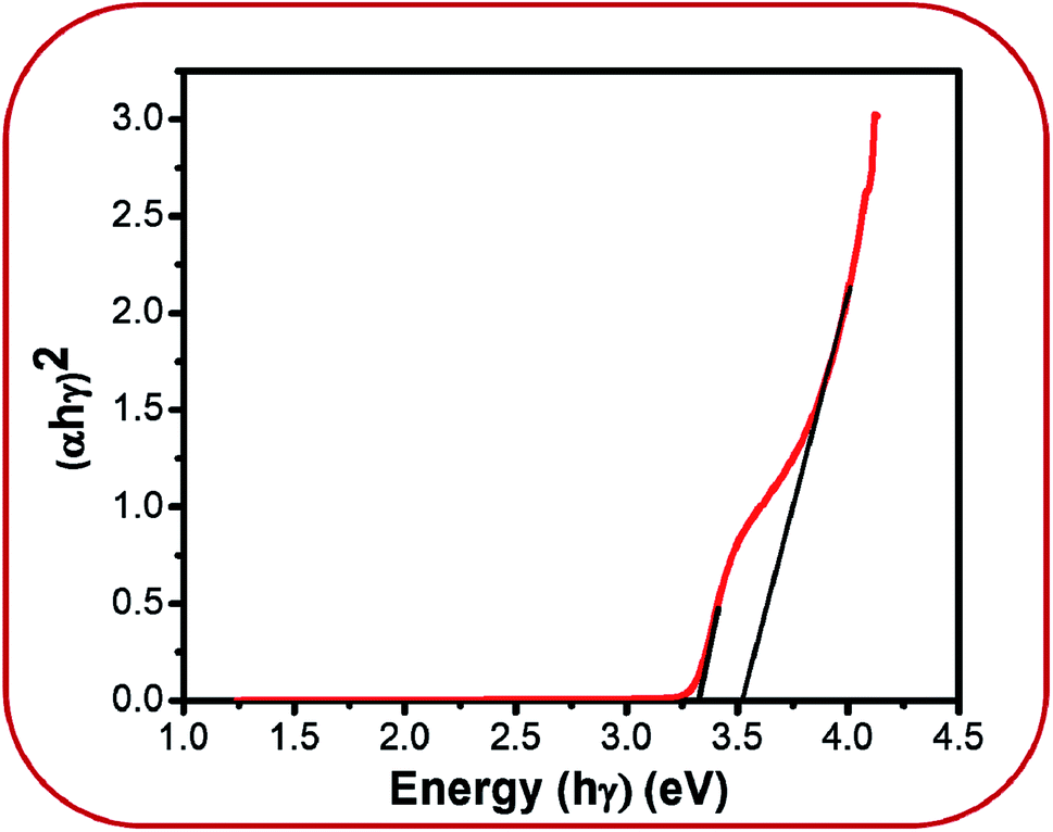 | ||
| Fig. 6 UV-Vis plot of BZ150. | ||
The visible spectra of BZ150 to BZ750 samples can be deconvoluted into 3 peaks using Gaussian equation, whereas that of BZ850 sample can be deconvoluted into 2 such peaks. The peak positions and their respective intensities derived from the Gaussian fittings have been listed in Table 3.
| Sample | Peak 1 (nm) | Intensity (×106) | Peak 2 (nm) | Intensity (×106) | Peak 3 (nm) | Intensity (×106) |
|---|---|---|---|---|---|---|
| BZ150 | 441 | 6.14 | 610 | 13.7 | 752 | 4.1 |
| BZ350 | 444 | 5.63 | 619 | 13.8 | 755 | 4.31 |
| BZ450 | 453 | 2.82 | 613 | 7.6 | 756 | 2.24 |
| BZ550 | 451 | 3.2 | 605 | 7.17 | 758 | 2.0 |
| BZ650 | 441 | 0.201 | 606 | 0.307 | 773 | 0.131 |
| BZ750 | 441 | 0.195 | 591 | 0.267 | 766 | 0.079 |
| BZ850 | 438 | 0.107 | 577 | 0.240 | — | — |
Fig. 7 shows the deconvoluted PL peaks for all the samples. It is observed that, the first peaks of all the samples are narrow and centered around 430–450 nm causing blue emission (ref. Table 3). The peaks for all the samples lying between 430–450 nm are attributed to the direct recombination of photogenerated electrons trapped in the neutral and charged Zni defect states with the holes in the valence band.41 The oxygen rich precursors are believed to have triggered the formation of this defect.24 Zni is a shallow donor level lying ∼0.4 eV below the conduction band.42 We believe that Zni and excited Zni (ex-Zni) form an almost continuous defect band designated as extended Zni band. Therefore, in all the samples the positions of blue emission peaks are slightly different from each other. Considering the fact that blue emission peaks of all the samples lie between 430–450 nm, we have calculated the width of the extended Zni band to be approximately 0.4 eV. This seems likely in view of the fact that in insulating materials such as MgO the width of point defect bands were found to be in the order of 1 eV.43
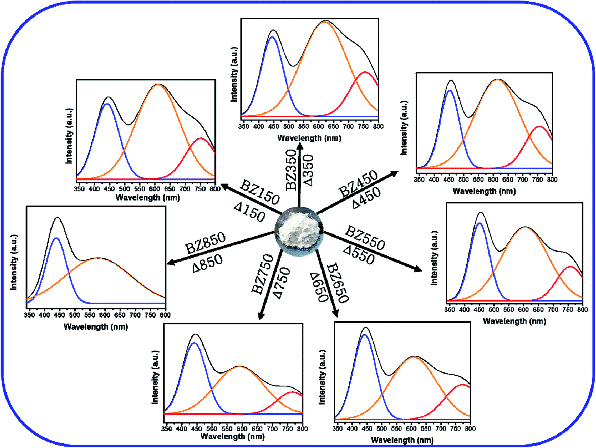 | ||
| Fig. 7 Deconvoluted PL patterns of BZ150, BZ350, BZ450, BZ550, BZ650, BZ750, and BZ850 samples. | ||
From the above discussion it may be concluded that photogenerated electrons from conduction band take a non-radiative tour to the extended Zni defect band and thereafter jump to the valence band with a blue emission to recombine with a hole. This is diagrammatically shown in Fig. 8.
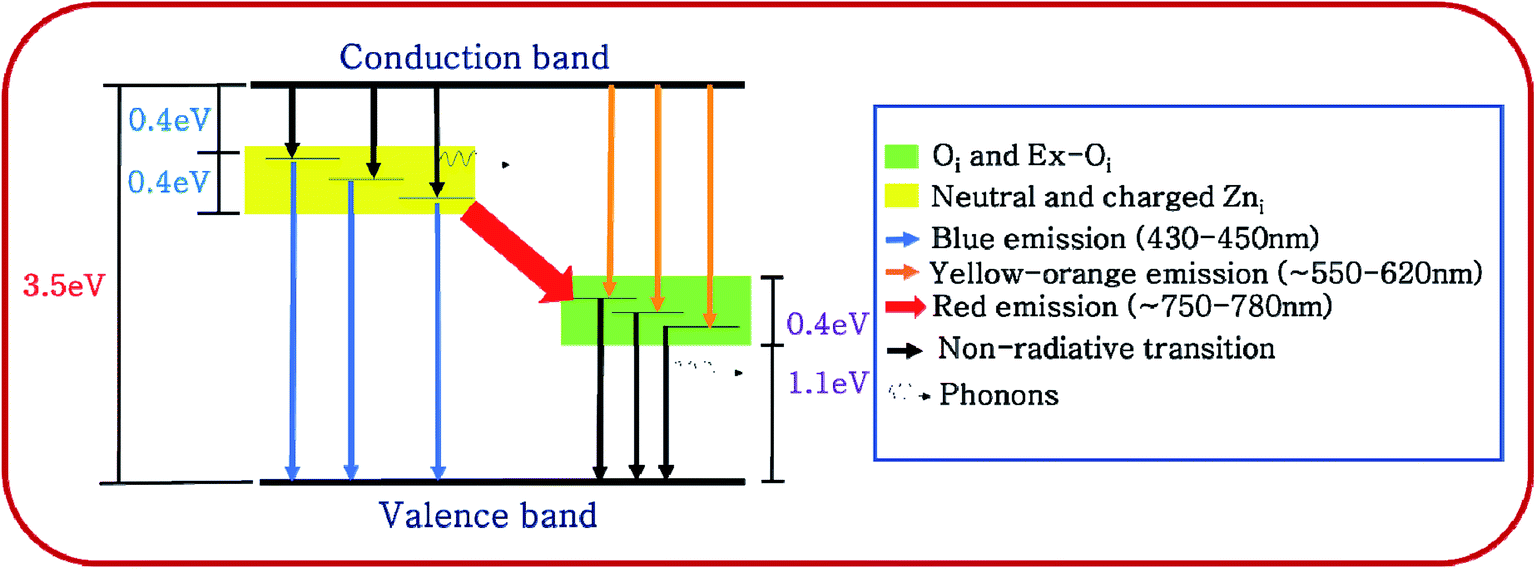 | ||
| Fig. 8 Proposed band diagram of ZnO samples (BZ150–BZ850) including the defect bands. | ||
For BZ150, BZ350, BZ450, BZ550, BZ650 and BZ750 samples the second peaks lie between 620–590 nm and cause yellow-orange emission (ref. Fig. 7 and Table 3). For BZ850 the second peak lies at 577 nm (ref. Fig. 7 and Table 3). The broad peaks lying in the region of 600–625 nm are attributed to the neutral and charged Oi defects.20 As discussed earlier, the presence of oxygen interstitial defects has also been established by Raman and EDX studies. The origin of this defect may be traced back to the oxygen rich precursors.24 From literature it was found that, it is a deep-seated acceptor level lying 1.1 eV above the valence band.42 We believe that Oi along with excited Oi (ex-Oi) forms a defect band designated here as extended Oi band. Considering the fact that the yellow-orange emission peaks for all the samples lie between 550–620 nm, the width of the band is calculated to be ∼0.4 eV and this seems logical considering the same fact that was taken into account while discussing the width of extended Zni band.43 Photogenerated electrons in the conduction band recombines radiatively with the holes present in the extended Oi band, thereby giving rise to the yellow-orange emission (ref. Fig. 8). Since, this radiative recombination involves a defect band of substantial width instead of a particular defect state, there are sample to sample variations in the positions of the yellow orange emission peak centers. The electrons trapped in the extended Oi band travel to the valence band by a non-radiative transition (ref. Fig. 8).
With increasing annealing temperature, the concentration of the Oi and ex-Oi defects reduce. Therefore, the width of the ex-Oi defect band decreases, and the average energy gap between the defect band and conduction band increases. Therefore, the yellow-orange emission shifts towards higher energy side leading to a blue-shift in peak-2.
Finally, for BZ150, BZ350, BZ450, BZ550, BZ650 and BZ750 samples the third peaks lie between 750–780 nm and cause red emission. Plausibly, there is a non-radiative transition of the photogenerated electrons from the conduction band to the extended Zni band followed by a radiative transition to the extended Oi band causing red emission, and finally another non-radiative transition to valence band (ref. Fig. 8). In BZ150, BZ350, BZ450, BZ550, BZ650 and BZ750 samples the wavelength of red emission is such that it matches well with the energy difference of the extended Zni and extended Oi bands.
Additionally, it may be noted that for BZ850 sample the red emission is invisible. Fig. 5 clearly depicts that the intensity of all the emissions are decreasing with increasing annealing temperature i.e. defects are being gradually eliminated. It might be possible that in BZ850 sample the intensity of red emission has reduced to such an extent that the overwhelming tail of the yellow-orange emission has completely masked the red emission.
Peak-3 evolves as a result of transition of electrons from ex-Zni defect band to ex-Oi defect band. The minimum energy possible for this emission is 1.2 eV corresponding to an emission wavelength of ∼1033 nm and the maximum energy possible is 2 eV corresponding to an emission wavelength of ∼620 nm for BZ150 sample (ref. Fig. 8). However, at higher temperatures the ex-Oi defect band shrinks and hence the minimum energy increases and consequently the wavelength possible for this emission shifts to ∼885 nm. Since, at higher temperatures the emission in IR region significantly shifts towards the red region, more energies of higher wavelength emissions are added to peak-3. In other words, strong tails of IR emission(s) merge with peak-3. Thus, due to the increasing addition of energies of higher wavelengths to the red emission the peak at ∼757 nm shifts towards higher wavelength (∼775 nm). This explains the red shift of peak-3.
Annihilation of defect is a diffusion-controlled process. At lower annealing temperatures (150 °C and 350 °C) diffusion kinetics of the defects is slow and hence defects were not annihilated significantly. Therefore, PL intensity did not change much from BZ150 to BZ350 sample.
However, at higher temperatures (above 350 °C) the rate of diffusion of the defects increases leading to a faster annihilation of the defects. Therefore, PL intensity reduced sharply from BZ350 to BZ450.
However, PL intensity did not reduce appreciably from BZ450 to BZ550. At higher temperatures rate of defect annihilation indeed increases. However, with increasing temperature the ionization of the neutral defects also increases. At lower temperatures the rate of ionization is negligible owing to unavailability of sufficient ionization energy. At sufficiently high temperatures ionization energy is available. However, at such high temperatures both ionized and neutral defects are annihilated owing to very high diffusivity. Therefore, PL intensity reduces sharply from BZ550 to BZ650.
The ionic lattice of ZnO poses an electrical potential field through which both neutral and ionized defects must move in order to diffuse to the surface. The ionized defects being charged species have stronger interaction with this field as compared to the neutral defects. Therefore, the activation energy barriers for the diffusion of these ionized defects are higher than those of neutral defects. At moderately high temperatures energy available is comparable to the activation energy barrier for the diffusion of neutral defects but is lower than that of the charged defects. Therefore, at such temperatures some of the neutral defects will be stabilized by ionization and hence rate of annihilation would reduce. This is what is observed at BZ550 as the PL intensity does not reduce comprehensibly from BZ450 to BZ550.
Plausible mechanism for the formation of oxygen interstitial (Oi) and excited oxygen interstitial (ex-Oi). It may be noted that Zni defect is common place but Oi defect is relatively rare. Also, the generation of Oi involves high energy as it is a deep-seated defect level and hence it is bizarre that at such low synthesis temperature Oi defects will be formed. Here we have come up with a logical reaction mechanism for the generation of Oi defect states during the synthesis.
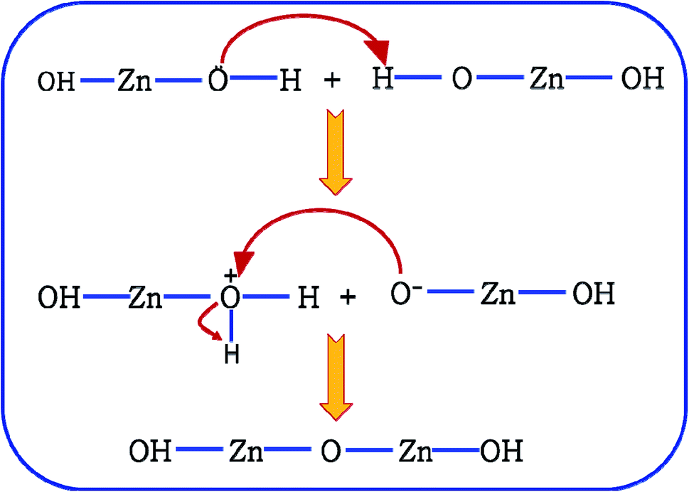
It is proposed that Oi and ex-Oi defects from during the nucleation growth of ZnO from the precursor salt. Zinc nitrate, when refluxed in ammoniacal water (∼10 pH) it initially produces zinc hydroxide with the chemical formula of Zn(OH)2. Oxygen atom in Zn(OH)2 has extra pair of electrons. Hence, O atom, a nucleophile from one Zn(OH)2 molecule attacks the H atom (electrophilic centre) of another Zn(OH)2 molecule in near proximity. This reaction involves the formation of two intermediate species viz. OH–Zn–O− and H2O+–Zn–OH. The nucleophilic centre of OH–Zn–O− (O−) attacks the electrophilic centre (Zn) of H2O+–Zn–OH leading to the elimination of one water molecule, leading to the condensation product of OH–Zn–O–Zn–OH. This reaction continues to form ZnO particles. This condensation process is schematically delineated in Fig. 9. This mechanism is an extension of the mechanism of water condensation of Si(OH)4 to form –Si–O–Si– under basic condition.44
 | ||
| Fig. 9 Mechanism of condensation of Zn(OH)2. | ||
This mechanism is now further extended to explain the presence of Oi and ex-Oi defects in the precipitate. During nucleation and growth phase lots of OH− are available owing to highly basic condition and the O atoms in that behave as nucleophiles. At the same time the Zn ion of the condensation product, OH–Zn–O–Zn–OH attains partial positive charge as its electron clouds shift towards the adjacent O atoms having high electronegativity. These Zn atoms behave like electrophilic centres and get attacked by the nucleophilic oxygen atom of a hydroxyl ion, thereby forming a weak electrostatic bond amongst them. This scenario is schematically depicted in the first step of Fig. 10a. Nucleophilic oxygen of one such weakly bonded hydroxyl ion attacks the hydrogen atom of another such hydroxyl ion in the vicinity to form an intermediate species. This species then loses the water molecule. The doubly charged oxygen atom shown in the third step of Fig. 10a will be found in the final ZnO lattice as 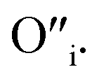 The size of oxygen atom is very small, the precipitation of ZnO involves nucleation and growth, and nuclei are extremely small in size providing very high surface areas. Therefore, it is plausible that a myriad of such
 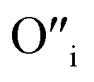 will get entrapped in the ZnO lattice during the nucleation and growth stage. Also due to the small size of the nuclei during precipitation, there would be a substantial amount of Zn terminated species such as, Zn+–O–Zn–OH etc. Such species will lead to the formation of
  and Oi as shown in Fig. 10b and c, respectively. Thus, the above is the plausible mechanism for the generation of very large concentrations of Oi and ex-Oi defects during precipitation of ZnO.
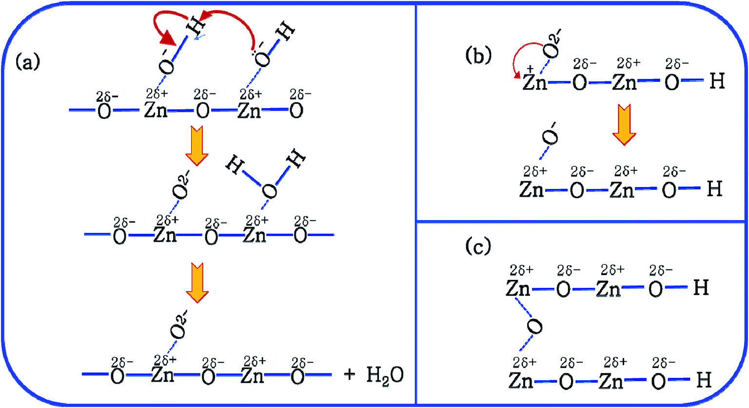 | ||
Fig. 10 Mechanism of formation of (a)  (b) (b)  and (c) Oi. and (c) Oi. | ||
Plausible mechanism for the formation of zinc interstitial (Zni) and excited zinc interstitial (ex-Zni). The size of the Zn2+ (0.74 Å) is smaller than O2− (1.42 Å). Secondly, during precipitation of ZnO nuclei formed are extremely small and consequently highly energetic. Being smaller, the energy barrier of migration of Zn2+ to the interstitial sites would be small and secondly nuclei being highly energetic, effective energy barrier would further be reduced than that of the bulk. Thus, one would expect the formation of more of Zni by Frenkel mechanism during the course of precipitation via the nucleation growth process. Subsequently, Zni could be ionized to form ex-Zni. Thus the mechanism of generation of Zni and ex-Zni could be represented as follows:
| ZnZn = Zni + VZn | (1) |
The transition of one or two electrons from Zni to the conduction band gives rise to  and
and  and can be given by,
 | (2a) |
 | (2b) |
Determination of CIE-coordinates and corresponding correlated colour temperature (CCT). The CIE plots of all the samples from BZ150 to BZ850 are shown in Fig. 11. The corresponding chromaticity coordinates (X, Y) are tabulated in Table 4. These coordinates were used to calculate the correlated color temperature (CCT) of all the samples following McCamy's relation,45 given by, CCT = 449n3 + 3525n2 + 6823.3n + 5520.3, where n = (X − 0.3320)/(0.1858 − Y). The correlated colour temperatures (CCT) (ref. Table 4) ensure that the emissions corresponding to all the samples are cool in nature as all the CCT values are more than 4000 K. This result is important as in LED based applications cool light is preferred.
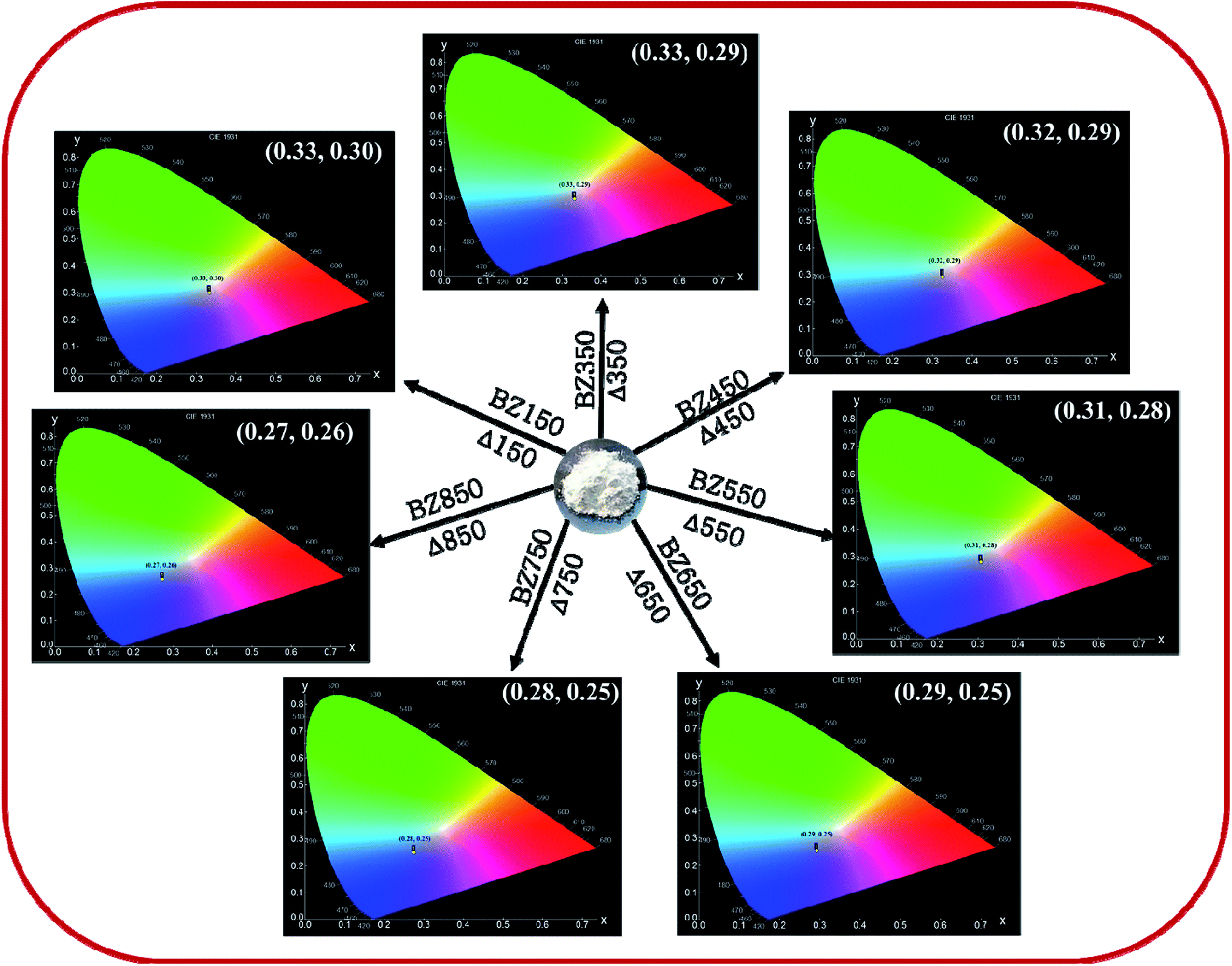 | ||
| Fig. 11 CIE plots of BZ150, BZ350, BZ450, BZ550, BZ650, BZ750, and BZ850 samples. | ||
| Sample | X | Y | CCT (K) |
|---|---|---|---|
| BZ150 | 0.33 | 0.30 | 5641 |
| BZ350 | 0.33 | 0.29 | 5651 |
| BZ450 | 0.32 | 0.29 | 6352 |
| BZ550 | 0.31 | 0.28 | 7311 |
| BZ650 | 0.29 | 0.25 | 11616 |
| BZ750 | 0.28 | 0.25 | 13585 |
| BZ850 | 0.27 | 0.26 | 13936 |
Whereas, the chromaticity co-ordinates of BZ150, BZ350 and BZ450 sit on the edge of the white spot in the CIE plot, chromaticity co-ordinates of BZ550, BZ650, BZ750, and BZ850 are clearly blue shifted. Fig. 12a shows that annealing of the as prepared ZnO sample at various temperatures from 150 °C to 850 °C in ordinary air atmosphere causes the intensity of yellow-orange emission to reduce at a much faster rate than that of blue emission. Hence, it might be expected that the CIE co-ordinates will be blue shifted and exactly that has happened. The reason for faster decay of yellow-orange emission with respect to blue emission can be explained with the diffusion kinetics of Oi and Zni defects.
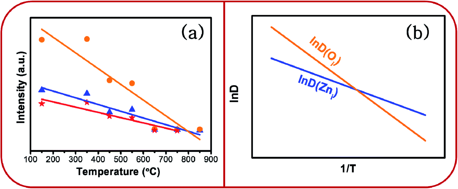 | ||
| Fig. 12 (a) Dependence of PL intensity of ZnO samples on annealing temperature and (b) schematic plot of lnD vs. 1/T. | ||
Evidently, with increasing temperature of annealing the Oi defect responsible for yellow-orange emission is annihilated at a much faster rate than the Zni defect responsible for the blue emission. The activation energy barrier to diffusion of Zni (QZni) is only about 0.3–0.5 eV.46–48 Since the size of O2− (1.42 Å) is much bigger than that of Zn2+ (0.74 Å), it might be expected that the activation energy barrier to the diffusion of oxygen interstitial (QOi) is higher than QZni. The temperature dependent variation of diffusion coefficient of Oi (D(Oi)) and Zni (D(Zni)) would be given by,
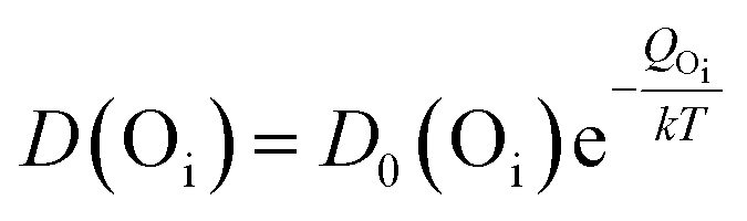 | (3) |
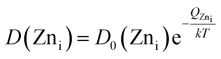 | (4) |
Fig. 12b gives the schematic plot of lnD vs. 1/T.
From the plot it is observed that lnD(Oi) increases at a much faster rate than lnD(Zni) with the increase in temperature. Therefore, diffusion flux J(Oi) would increase at a much faster rate than J(Zni) with increasing temperature. Therefore, the Oi defects would be annealed much faster than the Zni defects, especially at higher temperatures. This is observed in Fig. 12a.
However, this analysis does not answer the question why high temperature annealing under ordinary atmosphere reduces the intensity of the oxygen interstitial defects. It has already been explained in an earlier section that Oi and charged Oi was generated by a non-equilibrium process during the precipitation of ZnO by the process of nucleation. Now if this Oi concentration was to be in equilibrium with the partial pressure of oxygen, pO2 according to the following equation:
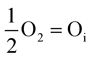 | (5) |
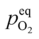 would be given by,
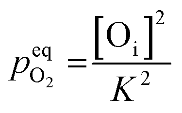 | (6) |
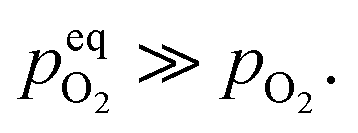 Therefore, eqn (5) should be driven in the backward direction in order to achieve
 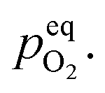 However, at lower temperature this [Oi] is stabilized by slow kinetics of diffusion. When the samples are heat treated in ordinary atmosphere at higher temperatures the diffusion kinetics of Oi becomes sufficiently fast resulting in the decrease of the [Oi]. Increasing temperature will enhance this process exponentially (ref. eqn (3)), thereby accounting for the drastic fall in the intensity of the Oi. Similar argument will be held true for ex-Oi. The decrease in the intensity of blue emission due to Zni and ex-Zni defects as a function of heat treatment of the samples at higher temperature in ordinary atmosphere could also be explained by similar arguments as delineated above.
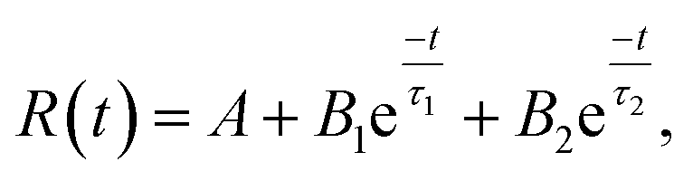 | (7) |
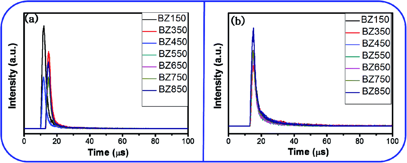 | ||
| Fig. 13 Time decay plots of the (a) the blue emission and (b) the yellow-orange emission of the BZ150, BZ350, BZ450, BZ550, BZ650, BZ750, and BZ850 samples. | ||
| Sample | Blue (nm) | τ1 (μs) | B1 | τ2 (μs) | B2 | QY (%) |
|---|---|---|---|---|---|---|
| BZ150 | 441 | 1.367 | 2208.197 | 9.128 | 129.760 | 13.0 |
| BZ350 | 444 | 1.433 | 1741.3 | 10.0 | 82.630 | 12.53 |
| BZ450 | 453 | 1.382 | 1139.285 | 9.533 | 64.850 | 12.66 |
| BZ550 | 451 | 1.414 | 1129.059 | 11.64 | 56.410 | 10.83 |
| BZ650 | 441 | 1.35 | 1139.646 | 9.643 | 56.071 | 12.28 |
| BZ750 | 441 | 1.35 | 1112.056 | 10.0 | 50.849 | 11.89 |
| BZ850 | 438 | 1.312 | 1461.115 | 10.0 | 68.224 | 11.6 |
| Sample | Yellow-orange (nm) | τ1 (μs) | B1 | τ2 (μs) | B2 | QY (%) |
|---|---|---|---|---|---|---|
| BZ150 | 610 | 1.151 | 553.147 | 11.86 | 142.21 | 8.84 |
| BZ350 | 619 | 1.707 | 630.283 | 14.1 | 114.04 | 10.79 |
| BZ450 | 614 | 1.326 | 700.916 | 10.63 | 154.32 | 9.42 |
| BZ550 | 605 | 1.41 | 952.777 | 9.445 | 146.956 | 12.9 |
| BZ650 | 606 | 1.595 | 906.816 | 10 | 121.512 | 13.75 |
| BZ750 | 591 | 1.67 | 936.85 | 10.15 | 184.4 | 14.12 |
| BZ850 | 577 | 1.434 | 1089.387 | 10 | 202.128 | 12.54 |
The average decay time periods of the blue emissions for BZ150, BZ350, BZ450, BZ550, BZ650, BZ750, and BZ850 samples are calculated as 3.55 μs, 3.56 μs, 3.68 μs, 4.4 μs, 3.51 μs, 3.54 μs, and 3.59 μs, respectively. Similarly, the average decay time periods of the yellow-orange emissions of BZ150, BZ350, BZ450, BZ550, BZ650, BZ750, and BZ850 samples are computed as 8.9 μs, 9.13 μs, 7.27 μs, 5.49 μs, 5.43 μs, 6.29 μs, and 6.26 μs, respectively. However, decay time periods for the red emission could not be determined as the intensity of the red emission was too low. It is to be noted that the integrated PL intensities of blue and red emissions (ref. Table 3) are comparable. However, the peak for blue emission is sharp and tall whereas the peak for red emission is diffused and short. Therefore, the peak intensity at the center of the peak is much higher for the blue emissions as compared to the red emissions. Time resolved PL is measured at the center of the peaks only. Therefore, τ-PL for blue emission could be measured whereas that of red emission could not be.
Calculation of quantum yield. The quantum yields (QY) of the samples were calculated using the following equation,
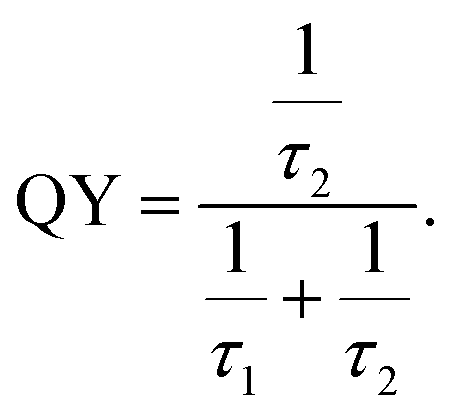 | (8) |
The QYs of the samples for the blue emissions and yellow-orange emissions are tabulated in Tables 5 and 6, respectively.
These QY values are comparable to those of the ZnO based materials reported earlier, viz. 15–21% in solid ZnO quantum dots,49 3–5% in ZnO quantum dots dispersed in ethanol,50 1.6% corresponding to the excitonic emission in bulk ZnO,51 12.7–15.2% corresponding to the visible emission in bulk ZnO15 etc.
Defects (Zni, Oi etc.) act as trap states for photogenerated electrons. Photogenerated electrons are trapped in those defect states. Eventually, those electrons recombine with the holes, both by radiative and non-radiative means. Consequently, there would be radiative and non-radiative recombination times given by τ2 and τ1, respectively. Now, eqn (8) clearly suggests that τ2 and τ1 determine the QY and these parameters may or may not vary with PL intensity. It should be noted that in this case annealing temperature has prominent effect on PL intensity (ref. Table 3) but negligible effect on τ2 and τ1 (ref. Tables 5 and 6). That is why QY here remains nearly unchanged irrespective of PL intensity.
The nanoparticles reported in here are mostly large in size which is corroborated by both FESEM and BET studies. This has an important implication on the long-term stability of the phosphorescence reported herein. It has already been stated that defect annihilation is a diffusion-controlled process and the defects (Oi and Zni) have to diffuse to the surface of the nanoparticles in order to get annihilated. Owing to the large particle size the diffusion length becomes very high. Therefore, the rate of defect annihilation reduces greatly. Further, the rate of defect annihilation is negligible in all the annealed samples (BZ150 to BZ850) at room temperature because low thermal energy is available at room temperature. This in turn would ensure the long-term stability of the defect mediated PL.
Conclusions
In summary, we have systematically studied the effect of annealing temperature on the blue phosphorescence in ZnO nanopowder. ZnO nanopowder was prepared by a facile, and cost-effective solution-precipitation method. The prepared nanopowders annealed at different temperatures were characterized by XRD, FESEM, EDX, BET, and micro-Raman spectroscopy to have an insight into the microstructure of the material. Photoluminescence emission spectra of these samples revealed the presence of blue, yellow, and red components originating from crystalline point defects, viz. zinc interstitial (Zni), and oxygen interstitial (Oi). A mechanism explaining the origin of such defects has been proposed. The concentrations of these defects and the intensity of the corresponding PL emission peaks varied as a function of annealing temperature. The corresponding CIE plots revealed that the overall color of emission gradually turned from light blue (CIE co-ordinate: (0.33, 0.30)) to dark blue (CIE co-ordinate: (0.27, 0.26)) as the annealing temperature increased from 150 °C to 850 °C. A thermodynamic interpretation to such variance in defect concentration has been proposed. τ-PL study and correlated color temperature (CCT) calculations ensured phosphorescence (decay time ∼9–12 μs) and cool lighting (CCT ∼ 5000–14000 K) in all the samples. Finally, all the samples exhibited comparable quantum yields with respect to previous ZnO based phosphorescence reports. This study suggests that thermal annealing can potentially be a technique for precise tuning of defect-mediated phosphorescence.
Funding sources
This research did not receive any specific grant from funding agencies in the public, commercial, or not-for-profit sectors.Conflicts of interest
There are no conflicts of interest to declare.Acknowledgements
The authors are greatly indebted to Dr G. C. Das, Ex-Professor, Department of Metallurgical and Material Engineering, for helpful discussions. The authors acknowledge the instrumental facilities obtained from the Department of Metallurgical and Materials Engineering and School of Materials Science and Nanotechnology, Jadavpur University. The authors are also thankful to Dr Somnath Bandyopadhyay, Head, Functional Materials and Devices Division for extending moral support. The authors gratefully acknowledge the kind support of Director, CSIR-Central Glass and Ceramic Research Institute, Kolkata.References
- M. Qiao, B. Zhang, Z. Xiao, J. Fang, and Z. Li, Power Semiconductor Devices and IC's, ISPSD '08. 20th International Symposium, 18–22 May 2008, p. 52 Search PubMed
.
- A. Morell and N. El Khiati, Green Phosphors for Large Plasma TV Screens, J. Electrochem. Soc., 1993, 140, 2019–2022 CrossRef CAS
- N. Hirosaki, R.-J. Xie, K. Inoue, T. Sekiguchi, B. Dierre and K. Tamura, Blue-emitting AlN: Eu2+ nitride phosphor for field emission displays, Appl. Phys. Lett., 2007, 91, 061101_1–061101_3 CrossRef
- M. Leskela, Rare earths in electroluminescent and field emission display phosphors, J. Alloys Compd., 1998, 275–277, 702–708 CrossRef CAS
- H. Kamikubo, ZnO: Zn phosphor for vacuum fluorescent display, US Pat.5128063A, Nec Corporation, Japan, 1992 Search PubMed
- H. Morkoc, Nitride Semiconductor Devices: Fundamentals and Applications, Wiley-VCH, Weinheim, Germany 2013, ch. 7 Search PubMed
- W. W. Holloway and M. Kestigian, Optical Properties of Cerium-Activated Garnet Crystals, J. Opt. Soc. Am., 1969, 59, 60–63 CrossRef CAS
- J. M. Robertson, M. W. van Tol, W. H. Smits and J. P. H. Heynen, Colourshift of the Ce3+ emission in monocrystalline epitaxially grown garnet layers, Philips J. Res., 1981, 36(1), 15–30 CAS
- I. Provencio, I. R. Rodriguez, G. Jiang, W. P. Haye, E. F. Moreira and M. D. Rollag, A novel human opsin in the inner retina, J. Neurosci., 2000, 20(2), 600–605 CrossRef CAS
- K. Thapan, J. Arendt and D. J. Skene, An action spectrum for melatonin suppression: evidence for a novel non-rod, non-cone photoreceptor system in humans, J. Physiol., 2001, 535(1), 261–267 CrossRef CAS
- Z. C. Wu, J. X. Shi, J. Wang, M. L. Gong and Q. Su, A novel blue-emitting phosphor LiSrPO4:Eu2+ for white LEDs, J. Solid State Chem., 2006, 179, 2356–2360 CrossRef CAS
- Z. C. Wu, J. X. Shi, J. Wang, H. Wu, Q. Su and M. L. Gong, Synthesis and luminescent properties of SrAl2O4:Eu2+ green-emitting phosphor for white LEDs, Mater. Lett., 2006, 60, 3499–3501 CrossRef CAS
- S. H. M. Poort, W. Janssen and G. Blasse, Optical properties of Eu2+-activated orthosilicates and orthophosphates, J. Alloys Compd., 1997, 260, 93–97 CrossRef CAS
- J. K. Park, K. J. Choi, J. H. Yeon, S. J. Lee and C. H. Kim, Embodiment of the warm white-light-emitting diodes by using a Ba2+ codoped Sr3SiO5:Eu phosphor, Appl. Phys. Lett., 2006, 88, 043511_1–043511_3 Search PubMed
- Y. Dai, Y. Zhang, Q. K. Li and C. W. Nan, Synthesis and optical properties of tetrapod-like zinc oxide nanorods, Chem. Phys. Lett., 2002, 358, 83–86 CrossRef CAS
- N. K. Zayer, R. Greef, K. Rogers, A. J. C. Grellier and C. N. Pannell, In situ monitoring of sputtered zinc oxide films for piezoelectric transducers, Thin Solid Films, 1999, 352, 179–184 CrossRef CAS
- Ü. Özgür, Y. I. Alivov, C. Liu, A. Teke, M. A. Reshchikov, S. Dŏgan, V. Avrutin, S.-J. Cho and H. Morkoç, A Comprehensive Review of ZnO Materials and Devices, J. Appl. Phys., 2005, 98, 041301 CrossRef
- T. M. Børseth, B. G. Svensson and A. Y. Kuznetsov, Identification of oxygen and zinc vacancy optical signals in ZnO, Appl. Phys. Lett., 2006, 89, 262112_1–262112_3 CrossRef
- N. S. Parmar, L. A. Boatner, K. G. Lynn and J.-W. Choi, Zn Vacancy Formation Energy and Diffusion Coefficient of CVT ZnO Crystals in the Sub-Surface Micron Region, Sci. Rep., 2018, 8, 13446_1–13446_8 Search PubMed
- L. E. Greene, M. Law, J. Goldberger, F. Kim, J. C. Johnson, Y. Zhang, R. J. Saykally and P. Yang, Low-temperature wafer-scale production of ZnO nanowire arrays, Angew. Chem., 2003, 115, 3139–3142 CrossRef
- M. Liu, A. H. Kitai and P. Mascher, Point defects and luminescence centres in zinc oxide and zinc oxide doped with manganese, J. Lumin., 1992, 54, 35–42 CrossRef CAS
- X. L. Wu, G. G. Siu, C. L. Fu and H. C. Ong, Photoluminescence and cathodoluminescence studies of stoichiometric and oxygen-deficient ZnO films, Appl. Phys. Lett., 2001, 78, 2285–2287 CrossRef CAS
- S. A. Studenikin, N. Golego and M. Cocivera, Fabrication of green and orange photoluminescent, undoped ZnO films using spray pyrolysis, J. Appl. Phys., 1998, 84, 2287–2294 CrossRef CAS
- A. A. Sokol, S. A. French, S. T. Bromley, C. R. A. Catlow, H. J. J. van Dam and P. Sherwood, Point defects in ZnO, Faraday Discuss., 2007, 134, 267–282 RSC
- E. Rauwel, A. Galeckas, P. Rauwel, M. F. Sunding and H. Fjellvaag, Precursor-dependent blue-green photoluminescence emission of ZnO nanoparticles, J. Phys. Chem. C, 2011, 115(51), 25227–25233 CrossRef CAS
- Y. Gong, C. Zou and Y. Yao, et al., A facile approach to synthesize rose-like ZnO/reduced graphene oxide composite: fluorescence and photocatalytic properties, J. Mater. Sci., 2014, 49(16), 5658–5666 CrossRef CAS
- G. Singh, A. Choudhary and D. Haranath, et al., ZnO decorated luminescent graphene as a potential gas sensor at room temperature, Carbon, 2012, 50(2), 385–394 CrossRef CAS
- A. B. Djurišić, Y. H. Leung, K. H. Tam, L. Ding, W. K. Ge, H. Y. Chen and S. Gwo, Green, yellow, and orange defect emission from ZnO nanostructures: Influence of excitation wavelength, Appl. Phys. Lett., 2006, 88, 103107 CrossRef
- W. C. Zhang, X. L. Wu, H. T. Chen, J. Zhu and G. S. Huang, Excitation wavelength dependence of the visible photoluminescence from amorphous ZnO granular films, J. Appl. Phys., 2008, 103, 093718 CrossRef
- C. R. Garcia, J. Oliva, L. A. Diaz-Torres, E. Montes, G. Hirata, J. Bernal Alvarado and C. Gomez-Solis, Controlling the white phosphorescence ZnGa2O4 phosphors by surface defects, Ceram. Int., 2019, 45(4), 4972–4979 CrossRef CAS
- N. Ashkenov, B. N. Mbenkum, C. Bundesmann, V. Riede, M. Lorenz, D. Spemann, E. M. Kaidashev, A. Kasic, M. Schubert and M. Grundmann, Infrared dielectric functions and phonon modes of high-quality ZnO films, J. Appl. Phys., 2003, 93, 126–133 CrossRef CAS
- J. F. Scott, UV Resonant Raman Scattering in ZnO, Phys. Rev. B: Solid State, 1970, 2, 1209–1211 CrossRef
- H. Fukushima, T. Kozu, H. Shima, H. Funakubo, H. Uchida, T. Katoda and K. Nishida, Joint IEEE International Symposium on the Applications of Ferroelectric, International Symposium on Integrated Functionalities and Piezoelectric Force Microscopy Workshop (ISAF/ISIF/PFM), 24-27 May 2015 Search PubMed
- J. Wang, S. Hou, H. Chen and L. Xiang, Defects-Induced Room Temperature Ferromagnetism in ZnO Nanorods Grown from ε-Zn(OH)2, J. Phys. Chem. C, 2014, 118, 19469–19476 CrossRef CAS
- J. Das, S. K. Pradhan, D. R. Sahu, D. K. Mishra, S. N. Sarangi, B. B. Nayak, S. Verma and B. K. Roul, Micro-Raman and XPS studies of pure ZnO ceramics, Phys. B, 2010, 405, 2492–2497 CrossRef CAS
- S. Vempati, A. Shetty, P. Dawson, K. Nanda and S. B. Krupanidhi, Cobalt-doped ZnO nanowires on quartz: synthesis by simple chemical method and characterization, J. Cryst. Growth, 2012, 343(1), 7 CrossRef CAS
- R. Cusco, E. A. Llado, J. Ibáñez, L. Artús, J. Jiménez, B. Wang and M. J. Callahan, Temperature dependence of Raman scattering in ZnO, Phys. Rev. B: Condens. Matter Mater. Phys., 2007, 75, 165202-1–165202-11 CrossRef
- S. H. Jeong, J. K. Kim and B. T. Lee, Effects of growth conditions on the emission properties of ZnO films prepared on Si (100) by rf magnetron sputtering, J. Phys. D: Appl. Phys., 2003, 36, 2017–2020 CrossRef CAS
- S. Das, U. K. Ghorai, R. Dey, C. K. Ghosh and M. Pal, Novel multiple phosphorescence in nanostructured zinc oxide and calculations of correlated colour temperature, Phys. Chem. Chem. Phys., 2017, 19, 22995–23006 RSC
- Z. Jia, L. Yue, Y. Zheng and Z. Xu, Rod-like zinc oxide constructed by nanoparticles: synthesis, characterization and optical properties, Mater. Chem. Phys., 2008, 107, 137–141 CrossRef CAS
- H. Zeng, G. Duan, Y. Li, S. Yang, X. Xu and W. Cai, Blue Luminescence of ZnO Nanoparticles Based on Non-Equilibrium Processes: Defect Origins and Emission Controls, Adv. Funct. Mater., 2010, 20(4), 561–572 CrossRef CAS
- X. Liu, X. Xing, Y. Li, N. Chen, I. Djerdj and Y. Wang, Controllable synthesis and change of emission color from green to orange of ZnO quantum dots using different solvents, New J. Chem., 2015, 39, 2881–2888 RSC
- W. D. Kingery, H. K. Bowen and D. R. Uhlmann, Introduction to Ceramics, Wiley-Interscience Publications, NY, 2nd edn, 1975 Search PubMed
- C. J. Brinker and G. W. Scherer, Sol-Gel Science: The Physics and Chemistry of Sol-Gel Processing, Elsevier Publications, 1st edn, 2013 Search PubMed
- M. Rai, G. Kaur, S. K. Singh and S. B. Rai, Probing a new approach for warm white light generation in lanthanide doped nanophosphors, Dalton Trans., 2015, 44, 6184–6192 RSC
- G.-Y. Huang, C.-Y. Wang and J.-T. Wang, First-principles study of diffusion of zinc vacancies and interstitials in ZnO, Solid State Commun., 2009, 149, 199–204 CrossRef CAS
- P. Erhart and K. Albe, Diffusion of zinc vacancies and interstitials in zinc oxide, Appl. Phys. Lett., 2006, 88, 201918_1–201918_3 CrossRef
- A. Janotti and C. G. Van de Walle, Native point defects in ZnO, Phys. Rev. B: Condens. Matter Mater. Phys., 2007, 76, 165202_1–165202_22 CrossRef
- S. Das, C. K. Ghosh, R. Dey and M. Pal, Novel green phosphorescence from pristine ZnO quantum dots: tuning of correlated color temperature, RSC Adv., 2016, 6, 236 RSC
- D. Bera, L. Qian, S. Sabui, S. Santra and P. H. Holloway, Photoluminescence of ZnO quantum dots produced by a sol–gel process, Opt. Mater., 2008, 30, 1233–1239 CrossRef CAS
- N. S. Norberg and D. R. Gamelin, Influence of Surface Modification on the Luminescence of Colloidal ZnO Nanocrystals, J. Phys. Chem. B, 2005, 109, 20810–20816 CrossRef CAS
Footnote |
| † Electronic supplementary information (ESI) available. See DOI: 10.1039/d0ra04766j |
| This journal is © The Royal Society of Chemistry 2021 |