
Ultra-stable ZnO nanobelts in electrochemical environments†
Mengyu
Hong
ab,
Jingjing
Meng
ab,
Huihui
Yu
ab,
Junli
Du
ab,
Yang
Ou
ab,
Qingliang
Liao
ab,
Zhuo
Kang
 ab,
Zheng
Zhang
*ab and
Yue
Zhang
*ab
ab,
Zheng
Zhang
*ab and
Yue
Zhang
*ab
aBeijing Advanced Innovation Centre for Materials Genome Engineering, Beijing Key Laboratory for Advanced Energy Materials and Technologies, University of Science and Technology Beijing, Beijing 100083, People's Republic of China. E-mail: yuezhang@ustb.edu.cn; zhangzheng@ustb.edu.cn
bState Key Laboratory for Advanced Metals and Materials, School of Materials Science and Engineering, University of Science and Technology Beijing, Beijing 100083, People's Republic of China
First published on 26th October 2020
Abstract
Zinc oxide (ZnO) has been widely considered as a promising candidate in electro-chemical devices due to the high electrical transport performance and easy-fabrication. However, the active chemical properties of ZnO nanobelts restrict their application in practical electro-chemical devices. Here, we adopted an indium doping strategy to improve the corrosion resistance of ZnO nanobelts. Compared with other atomic doping methods, the indium doping method not only formed several layers of indium atoms in the body of ZnO nanobelts but also created a ZnxIn1−xO passivated layer on the ZnO nanobelt surface. After doping indium atoms into ZnO nanobelts, the self-corrosion potential increased and the self-corrosion current decreased which greatly reduced its corrosion rate in the electrochemical solution. Furthermore, the electrical transport properties of indium-doped zinc oxide (In–ZnO) nanobelts presented ultrahigh stability even after being soaked in the electrochemical solution for 43 hours. The enhanced anticorrosive quasi-2D ZnO nanobelts offer a promising development of ZnO-based electro-chemical devices.
1. Introduction
The ZnO nanostructure has a direct and wide bandgap (Eg = 3.37 eV at room temperature), large exciton binding energy (60 meV), remarkable electromechanical properties, piezoelectric properties, and good biocompatibility. In recent years, great breakthroughs have been achieved on ZnO nanomaterials and provide a positive application prospect in the fields of photoelectric information,1–8 energy conversion,9–19 storage,20–28 catalysis,29–31 biosensors,32–40 quantum applications,41–46 and intelligent systems, etc.ZnO is a reactive amphoteric oxide, which can easily react with and be corroded by acids and alkalis. The corrosion phenomenon of ZnO nanostructures has been easily observed in acidic, alkaline, and biological environments. It has become a research hotspot and has been widely studied.47–57 Degen et al.54 changed the pH value of the solution from 6 to 14 and found that the ZnO reacted differently with the solution and was corroded. ZnO was also corroded in biological environments as the interaction of ZnO wires with horse blood serum caused its degradation into mineral ions after a few hours.53 It even disappeared after soaking in deionized water for 15 hours.48 The extremely corrosive nature of ZnO greatly limits its use in a wide range of electro-chemical devices. To solve this problem, researchers have put much effort and most studies focused on structure design.58–67 Some used ZnO as the core covered by other materials, such as BiFeO3,62 Ta2O5,61 and TiO2,68etc. to form a cell-shell structure, or built a protective layer on ZnO made by chemical synthesis, spin coating, or atomic layer deposition (ALD). However, these methods have certain limitations, for instance, during the TiO2 deposition process on ZnO nanowires conducted by ALD, the corrosion of ZnO can be aggravated by the reaction gas.68 Besides, when a shell is formed on the surface of one-dimensional photocorrosion sensitive materials such as ZnO, CdS, and PbS, the shell-enhanced photocorrosion effect is prone to affect their stability in photovoltaic devices.60 Previous researches, which used the first-principles calculations, has confirmed that indium doping greatly reduces the surface energy of ZnO. The surface energy decreases with the increasing number of doped indium atoms.69 Here, we experimentally proposed a new strategy to increase the anti-corrosion performance of ZnO nanobelts by doping indium atoms. We doped indium into ZnO nanobelts, the morphology, height, and electrical properties of indium-doped zinc oxide (In–ZnO) nanobelts remained stable after immersion in the electrochemical environment for a long time, the corrosion resistance of In–ZnO nanobelts has been improved significantly. The mechanism of the improvement of corrosion resistance has been explained through electrochemical experiments and first-principles analysis.
2. Results and discussion
2.1 Synthesis of In–ZnO nanobelts
The In–ZnO nanobelts were synthesized by the chemical vapor deposition (CVD) method. Firstly, the Zn powder (Aladdin, >99.99%), In2O3 powder (Aladdin, >99.99%), and C powder (Aladdin, >99.5%) were mixed with a molar ratio of 3![[thin space (1/6-em)]](https://www.rsc.org/images/entities/char_2009.gif) :1:2 as the precursor. Secondly, a 1 × 1 cm2 cleaned SiO2/Si (300 nm SiO2) substrate was filmed by Au through direct current sputtering. The 80 nm-thick Au film plays the role of catalyst in the growing process of In–ZnO nanobelts. After that, the SiO2/Si substrate was placed face-down on the porcelain boat which was loaded with the precursor. Then, the boat was put into the quartz tube furnace with a constant gas flow of 300 sccm Ar and 4.5 sccm O2. At the same time, the quartz tube was heated up to 980 °C. Under this circumstance, the reacting time of the precursor lasted for 15 min. Finally, the SiO2/Si substrate was cooled in the air to room temperature and the light-yellow In–ZnO nanobelts grew upon it. The In–ZnO nanobelts used in this work were grown using the same method described above.
:1:2 as the precursor. Secondly, a 1 × 1 cm2 cleaned SiO2/Si (300 nm SiO2) substrate was filmed by Au through direct current sputtering. The 80 nm-thick Au film plays the role of catalyst in the growing process of In–ZnO nanobelts. After that, the SiO2/Si substrate was placed face-down on the porcelain boat which was loaded with the precursor. Then, the boat was put into the quartz tube furnace with a constant gas flow of 300 sccm Ar and 4.5 sccm O2. At the same time, the quartz tube was heated up to 980 °C. Under this circumstance, the reacting time of the precursor lasted for 15 min. Finally, the SiO2/Si substrate was cooled in the air to room temperature and the light-yellow In–ZnO nanobelts grew upon it. The In–ZnO nanobelts used in this work were grown using the same method described above.
2.2 Characterization of In–ZnO nanobelts
The scanning electron microscopy (SEM) was used to characterize the morphology of In–ZnO nanobelts prepared by the CVD method, as shown in Fig. S1(a and b) (ESI†). It can be seen that the nanobelts have good uniformity. The Auger electron spectrum (AES) and energy dispersive spectroscopy (EDS) results (Fig. 1) indicate that the indium indeed exists in In–ZnO nanobelts. The X-ray photoelectron spectroscopy (XPS) method was used to analyze the composition and chemical state of the In–ZnO. The atomic concentrations of Zn, In, and O estimated in this experiment were 30.81%, 7.55%, and 61.64%, respectively. The ratio of oxygen atoms was high, mainly because of the adsorption of oxygen under the non-vacuum situation. The XPS spectral shown in Fig. S1(e) (ESI†) indicated that indium atoms and oxygen atoms had formed chemical bonds.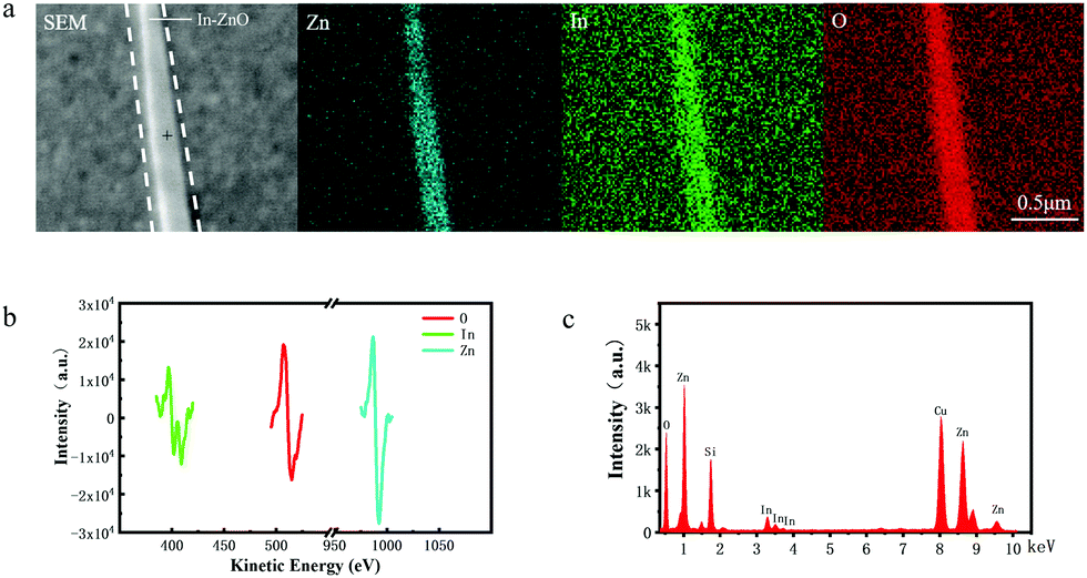 | ||
| Fig. 1 The morphology and composition characterization of In–ZnO nanobelts. (a) The SEM image and the AES elemental mapping images of Zn, In, and O of the In–ZnO nanobelt. (b) The AES spectrum of the In–ZnO nanobelt on the silicon substrate. (c) The EDS spectrum of In–ZnO nanobelts on the copper grid. | ||
2.3 Morphological stability of In–ZnO nanobelts in acids
The hydrochloric acidic solution (HCl) is a typical electrochemical environment. The hydrochloric acidic solution of pH 6 was used to simulate the electrochemical environment in this work. In–ZnO nanobelts were soaked into the HCl solution to study the morphological stability. A unique clean-dry transfer method was used in this experiment to avoid the effects of liquid. The targeted clean SiO2/Si (300 nm SiO2) substrate B was put face-down squarely on the SiO2/Si substrate A (growing with the In–ZnO nanobelts), and then gently rub the substrate B along the surface of substrate A to transfer the sample (the schematic processes are shown in Fig. S2, ESI†). Then, the SiO2/Si substrate B with In–ZnO nanobelts was carefully soaked into HCl solution for a certain time. After that, the SiO2/Si substrate B was removed and cleaned with deionized water for more than 5 times. Then the samples should be dried by N2 as soon as possible to reduce the influence of deionized water. The surface morphology of In–ZnO nanobelts stayed intact after being placed in the HCl solution for 25 min. In Fig. 2(a), it shows that there was no obvious morphological corrosion phenomenon. A control group using pure ZnO nanobelts under the same conditions was also carried out. The surface of pure ZnO nanobelts became rough and the morphology was not uniform anymore after soaking in HCl solution for 25 min, as shown in Fig. 2(b).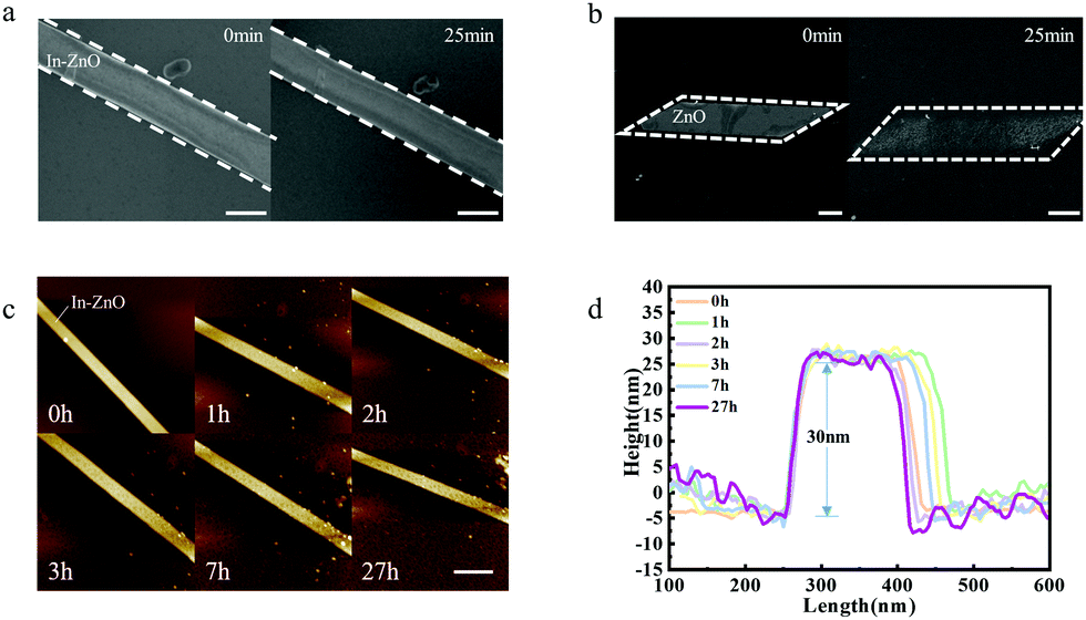 | ||
| Fig. 2 The morphology and height characterizations of In–ZnO nanobelts after corrosion in the acidic solution for different time lengths. (a and b) FE-SEM images of In–ZnO and pure ZnO nanobelts after corrosion for 0 min and 25 min. Scale bars = 20 μm. (c and d) AFM images and corresponding height profiles for different corrosion time lengths. Scale bar = 0.5 μm. | ||
To verify the morphological variation of In–ZnO nanobelts, the atomic force microscope (AFM) was employed. Soaked in HCl solution for several hours, the In–ZnO nanobelts generated negligible fluctuations in its height, and it still maintained about 30 nm even after 27 hours in acidic solution, as shown in Fig. 2(c and d). There is no doubt that indium doping could largely strengthen the structure stability of ZnO nanobelts in the electrochemical environment.
2.4 Electrical stability of In–ZnO nanobelts in acids
A single In–ZnO nanobelt field-effect transistor (FET) was constructed and tested to investigate its electrical performance in the HCl solution. The Cr/Au patterned surface of the insulating SiO2/Si (300 nm SiO2) substrate was processed by the ultraviolet lithography and thermal evaporation deposition. Then the In–ZnO nanobelts were dispersed on the insulating SiO2/Si substrate through the above-mentioned direct dry transfer method; among which, the nanobelts with intact morphology were chosen as the experiment samples. Next, the two ends of In–ZnO nanobelts were carefully fixed with Pt by the focused ion beam system (FIB). To avoid being affected by the acid on the contact electrodes, first, a layer of polymethyl methacrylate (PMMA) was coated on the entire film sample, and then a small area of the chosen In–ZnO nanobelt was exposed by the electron beam lithography (EBL) technology; meanwhile, the rest, including the electrodes, was still covered by PMMA to keep from the electrochemical environment.After that, the single In–ZnO nanobelt FET was soaked in HCl solution for a different corrosion time (Fig. 3(a and b)). The electrical transport property of the single In–ZnO nanobelt FET was tested by Keithley 4200 semiconductor tester. Soaked in HCl solution for different hours, the electrical transport property of the single In–ZnO nanobelt FET has tiny fluctuations yet has no obvious decrease. Fig. 3(c) shows the current–voltage (I–V) curves of the single In–ZnO nanobelt FET being soaked in the electrochemical environment for a different time. These I–V curves change little, while the appearance of slight rectification characteristic is likely caused by the Schottky barrier between In–ZnO and the platinum electrodes. The current variations at the bias voltage of ±1 V are plotted in Fig. 3(d) and it is clear to see that the current values tested in different soaking times are relatively stable. The current at a bias voltage of ±1 V kept about ±15 μA after 43 hour corrosion. Indicating a stable electric transport of In–ZnO under electrochemical environments.
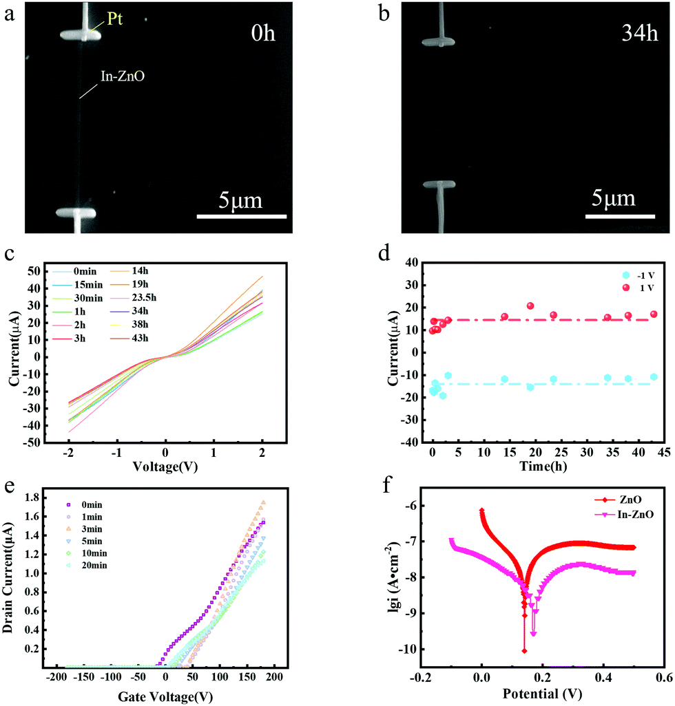 | ||
| Fig. 3 The electric transport performance analysis of In–ZnO nanobelts after corrosion in the acidic solution for different time lengths. (a) The original device structure diagram. (b) The morphology of the device after corroding in the acidic solution for 34 h. (c) The electrical transport property (I–V) curves for different corrosion time lengths. (d) The I–T curves at the potential of ±1 V for different corrosion time lengths. (e) The transfer characteristic curves of the In–ZnO nanobelts after different corrosion time lengths. (f) The Tafel polarization curves of the pure ZnO and In–ZnO nanobelts in the acidic solution of pH ≈ 6. | ||
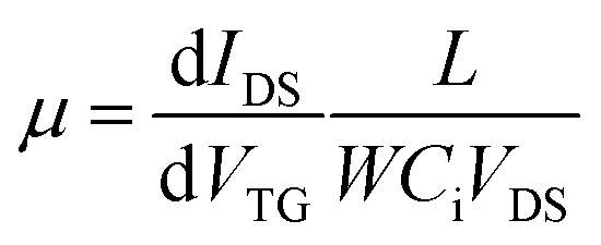
The transfer curves of the single In–ZnO nanobelt FET soaked in different time lengths are shown in Fig. 3(e). The slopes of the transfer characteristic curves show negligible variation. The carrier mobility calculated by the following formula fluctuates between 20 to 40 cm2 V−1 s−1, without the change in the order of magnitude.
 | (1) |
2.5 Anticorrosion mechanism of ZnO nanobelts in acids
An electrochemical experiment was adopted to investigate the difference in the self-corrosion potential (Ecorr) and self-corrosion current density (icorr) of pure ZnO and In–ZnO nanobelts. A three-electrode system was used to test the corrosion behaviour of the pure ZnO and In–ZnO nanobelts in HCl solution of pH ≈ 6. With a 1 × 1 cm2 area exposed to the acidic corrosive medium and the remainder were sealed with the epoxy resin adhesive, the as-grown nanobelts worked as a working electrode. The auxiliary electrode was a pure platinum electrode and the reference electrode was Ag/AgCl electrode. The experiments were conducted at room temperature in the acidic solution that did not exclude oxygen. Before the electrochemical tests, the open circuit potential–time curves of all samples were obtained after light-emitting for 10 min without applied voltage until the potential stabilized in the acidic solution. The potential dynamic scanning polarization curves were tested by an electrochemical workstation. The Tafel curves of the pure ZnO and In–ZnO nanobelts were obtained by scanning (scanning speed was 0.5 mV s−1) the open circuit near the potential range of ±250 mV as shown in Fig. 3(f). The Ecorr and icorr of pure ZnO nanobelts were 0.14 V and 17.8 nA cm−2, respectively. Under the same test condition, the Ecorr and icorr of In–ZnO nanobelts were 0.172 V and 3.16 nA cm−2. It is apparent that In–ZnO nanobelts have a higher Ecorr and lower icorr than pure ZnO nanobelts. The corrosion behaviour is unlikely to happen when the Ecorr value is getting increased or the icorr value reducing, thus, the above results demonstrate that the anticorrosion behaviour of ZnO nanobelts is strengthened by indium atom doping.Secondly, the atomic structure of In–ZnO nanobelts was investigated to further study the mechanism of the improving stability of In–ZnO nanobelts. The high-resolution transmission electron (HRTEM) image and selected electron diffraction image (Fig. 4(a and b)) show an excellent periodic lattice arrangement of the In–ZnO nanobelt. To further study its internal structure, the FIB technique with Pt used as a deposition source was used to cut the In–ZnO nanobelt and make a cross-sectional transmission electron microscopy (TEM) sample. Then, the atom arrangement of the In–ZnO nanobelt cross-section could be clearly observed in cross-sectional TEM images as shown in Fig. 5(a). In the high-angle annular dark-field scanning transmission electron microscopy (HAADF-STEM) images, the brightness of the atoms increases along with the rising ordinal number in the periodic table of elements. Therefore, the brighter atoms in Fig. 5(a) were indium atoms and the darker atoms were zinc atoms, while Oxygen atoms were too light to be examined by TEM. It shows the alternate stacking structures of one In–O layer and Zn–O layers stack along the c-axis ([0001] direction); the growing direction of In–ZnO nanobelt is vertical to the c-axis. It was recognized that the layered indium atoms were doped into the ZnO nanobelt and formed in a superlattice-like structure. In this selected ZnO nanobelt, four layers of indium atoms were inserted, and the rest zinc and oxygen atoms still maintained a perfect lattice arrangement. However, Fig. 5(a) indicates that the periphery of the sample, where the nanobelt is bonded to the SiO2/Si substrate and Pt deposits, is slightly brighter than the central portion of the nanobelt. This is attributed to the indium doped into the ZnO lattices. Subsequently, EDS analysis confirmed this speculation in Fig. 5(a–f). In Fig. 5(b), the content of indium in the orange rectangle area is significantly higher than that in the blue rectangle area. Fig. 5(f) is the line sweep curves of the sky-blue rectangle area in Fig. 5(a). It shows that, except for the four indium layers inserted into the nanobelt, the density of indium atoms on the top and bottom surfaces of the nanobelt has increased. It can also be inferred that the indium atoms added by doping tend to aggregate on the surface of nanobelt.
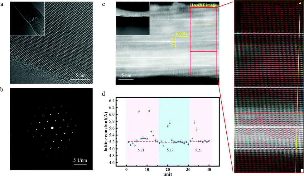 | ||
| Fig. 4 The TEM analysis of In–ZnO nanobelt. (a) The HRTEM image and the inset is the low-magnification TEM image of In–ZnO nanobelt. (b) The selected area electron diffraction (SAED) pattern of the as-synthesized In–ZnO nanobelt. (c) The HAADF cross-sectional image of In–ZnO nanobelt and the partial enlarged image. (d) The lattice constant curve from bottom to up of the cross-sectional of In–ZnO nanobelt. | ||
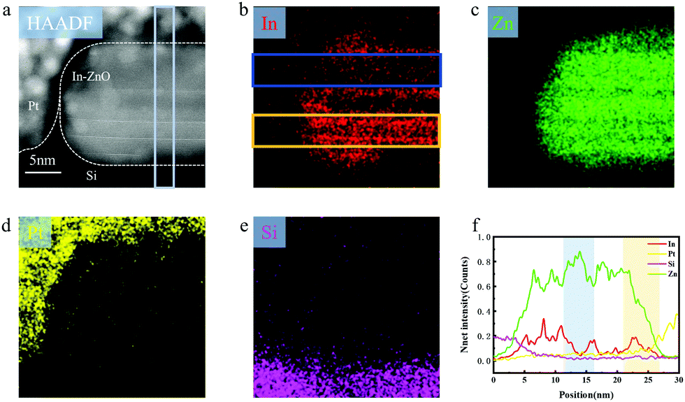 | ||
| Fig. 5 The cross-section analysis of the In–ZnO nanobelt. (a) The HAADF cross-sectional image of In–ZnO nanobelt and the corresponding EDS mapping of (b) In, (c) Zn, (d) Pt, and (e) Si. (f) The corresponding line sweep curves of the sky-blue rectangle area in (a). | ||
This phenomenon was also confirmed by measuring the change of the In–ZnO's lattice constants along the c-axis (indicated by the yellow arrow in Fig. 4(c)). The lattice constants of the upper and lower surface layers of the nanobelt (5.21 Å) are larger than the middle layers of the nanobelt (5.17 Å) (the influence of four inserted layers of indium atoms were eliminated) (Fig. 4(d)). It can be easily inferred that the indium atoms in the upper and lower surface layers of the nanobelt are more than that in the middle layers of the nanobelt. Because the radius of In element (the ionic radius is 0.81 Å, the covalent radius is 1.44 Å) is larger than that of Zn element (the ionic radius is 0.74 Å, the covalent radius is 1.22 Å), so the doping of indium element contributed to the stereo-hindrance effect.70–72 The stereo-hindrance effect would reduce the atomic interaction space and decrease the number of hydrogen ions that intruded into the internal structure during the corrosion process. Meanwhile, the ion-exchange became weaker, so that the corrosion rate decreased. This finding showed that the In–ZnO nanobelts formed a dense ZnxIn1−xO protective layer on the upper and lower surfaces and could protect In–ZnO nanobelts from being further corroded.
The occurrence of the corrosion behavior of ZnO nanobelts closely related to the hydrogen (H+) in the electrochemical environment, it has also been simulated in this work. The first-principles calculations were taken to explore the changes in the adsorption energy of ZnO nanobelts to hydrogen atom before and after indium doping. The adsorption energy refers to the part of energy released during the adsorption process. The larger adsorption energy, the easier the adsorption leading to heavier corrosion. The detailed calculation procedure is written in the methods section. An undoped pure ZnO model and a model in which indium atoms doped into ZnO by a layer form have been established to simulate the ZnO nanobelt in the experiment as closely as possible (as shown in Fig. 6). It is calculated that the adsorption energy of H atom of pure ZnO is 2.782 eV, while the adsorption energy of H atom of ZnO doped with a whole layer of indium atoms is reduced to 2.273 eV, and the adsorption energy is reduced by 0.509 eV. The large decrease in absorption energy means that H ions are less likely to react with ZnO and indicates an increasing resistance to the corrosion of ZnO in electrochemical solution. It also can explain the improvement of morphological and electrical stability of ZnO in electrochemical solution after indium atom doping.
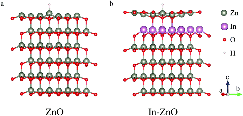 | ||
| Fig. 6 The calculation models of different indium atom doping concentrations. (a) The pure ZnO. (b) ZnO with a layer of Zn atoms substituted by indium atoms. | ||
3. Methods
The process of the first-principles calculations: the adsorption energy is calculated via density functional theory (DFT). A 2 × 2 × 1 supercell of ZnO was used to simulate the ZnO(0001) surface (as shown in Fig. 6a). A layer of Zn atoms was substituted by indium atoms to simulate the actual doping situation (as shown in Fig. 6b). The adsorption energy of considered heterostructures is calculated as follows:| Eb = |Etotal − (Ea + EZnO)| | (2) |
All the density-functional theory (DFT) computations were performed using the Cambridge Sequential Total Energy Package (CASTEP) based on the pseudopotential plane wave (PPW) method. Electron–ion interactions were described using the ultrasoft (USP) potentials. A plane-wave basis set was employed to expand the wave functions with a cutoff kinetic energy of 520 eV. For the electron–electron exchange and correlation interactions, the functional parametrized by Perdew–Burke–Ernzerhof (PBE), a form of the general gradient approximation (GGA), was used throughout. The van der Waals interaction was described using the DFT-D2 method proposed by Grimme.
During the geometry optimizations, the bottom atoms were fixed at the bulk position. In this work, the Brillouin-zone integrations were conducted using Monkhorst–Pack (MP) grids of special points. A (2 × 2 × 1) k-point grid was used for the model supercell. The self-consistent dipole correction was applied to eliminate the pseudo dipole interaction between the periodic images of the slab. The convergence criterion for the electronic self-consistent field (SCF) loop was set to 1 × 10⁻⁶ eV per atom. The atomic structures were optimized until the residual forces were below 0.01 eV Å−1.
Test characterization: the AES test was carried out by Scanning Auger Nanoprobe PHI710. The AFM measurements were performed with a Bruker Dimension Icon at room temperature in an atmospheric environment. The XPS analysis was carried out using Thermo Scientific ESCA Lab 250Xi XPS with a monochromatic KR Al X-ray line. The TEM and EDS characterization were carried out by FEI Titan G2 80-300 TEM/STEM. The Tafel curves were tested through the electrochemical workstation (CHI660C). Electrical analyses were performed using a Keithley 4200 semiconductor tester.
4. Conclusions
In this work, we fabricated In–ZnO nanobelts with perfect resistance to corrosion at the electrochemical environment. The In–ZnO nanobelts generated negligible fluctuations in its morphology and thickness after soaking for 27 hours in the electrochemical environment. By introducing the doped In atoms, the self-corrosion potential increased to 0.172 V and the self-corrosion current density decreased to 3.16 nA cm−2, which indicated an improvement in the anti-corrosion performance of In–ZnO nanobelts. Besides, the electric transport behaviors with the transfer characteristic curves and carrier mobility were relatively stable despite its immersion in the electrochemical solution. Furthermore, the theory calculation confirmed the anticorrosion mechanism of the In–ZnO, in which the indium doping decreases the adsorption energy of ZnO. This finding offers a promising opportunity to enhance the stability and prolongs the lifetime of ZnO-based nanodevices in the electrochemical environment.Conflicts of interest
There is no conflict to declare.Acknowledgements
This work was supported by the National Natural Science Foundation of China (Grant No. 51991340, 51991342, 51527802, 51972022, 51722203, 51672026), the Overseas Expertise Introduction Projects for Discipline Innovation (Grant No. B14003), the National Key Research and Development Program of China (Grant No. 2018YFA0703503, 2016YFA0202701), the Natural Science Foundation of Beijing Municipality (Grant No. Z180011), and the Fundamental Research Funds for the Central Universities (Grant No. FRF-TP-18-004A2, FRF-TP-18-001C1, FRF-TP-19-025A3).References
- J. Chang, Z. Lin, C. Zhu, C. Chi, J. Zhang and J. Wu, Solution-processed LiF-poped ZnO films for high performance low temperature field effect transistors and inverted solar cells, ACS Appl. Mater. Interfaces, 2013, 5, 6687–6693 CrossRef CAS.
- T.-S. Lin and C.-T. Leea, Homostructured ZnO-based metal-oxide-semiconductor field-effect transistors deposited at low temperature by vapor cooling condensation system, Appl. Surf. Sci., 2015, 354, 71–73 CrossRef CAS.
- S. Thiemann, M. Gruber, I. Lokteva, J. Hirschmann, M. Halik and J. Zaumseil, High-mobility ZnO nanorod field-effect transistors by self-alignment and electrolyte-gating, ACS Appl. Mater. Interfaces, 2013, 5, 1656–1662 CrossRef CAS.
- X. Zheng, Y. Sun, X. Yan, X. Chen, Z. Bai, P. Lin, Y. Shen, Y. Zhao and Y. Zhang, Tunable channel width of a UV-gate field effect transistor based on ZnO micro-nano wire, RSC Adv., 2014, 4, 18378 RSC.
- L. Chen, F. Xue, X. Li, X. Huang, L. Wang, J. Kou and Z. L. Wang, Strain-gated field effect transistor of a MoS2-ZnO 2D-1D hybrid structure, ACS Nano, 2016, 10, 1546–1551 CrossRef CAS.
- S. Liu, Q. Liao, Z. Zhang, X. Zhang, S. Lu, L. Zhou, M. Hong, Z. Kang and Y. Zhang, Strain modulation on graphene/ZnO nanowire mixed-dimensional van der Waals heterostructure for high-performance photosensor, Nano Res., 2017, 10, 3476–3485 CrossRef CAS.
- S. H. Shokouh, A. Pezeshki, S. R. Ali Raza, H. S. Lee, S. W. Min, P. J. Jeon, J. M. Shin and S. Im, High-gain subnanowatt power consumption hybrid complementary logic inverter with WSe2 nanosheet and ZnO nanowire transistors on glass, Adv. Mater., 2015, 27, 150–156 CrossRef CAS.
- F. Xue, L. Chen, J. Chen, J. Liu, L. Wang, M. Chen, Y. Pang, X. Yang, G. Gao, J. Zhai and Z. L. Wang, p-type MoS2 and n-type ZnO diode and its performance enhancement by the piezophototronic effect, Adv. Mater., 2016, 28, 3391–3398 CrossRef CAS.
- H. Dong, Y. Liu, J. Lu, Z. Chen, J. Wang and L. Zhang, Single-crystalline tower-like ZnO microrod UV lasers, J. Mater. Chem. C, 2013, 1, 202–206 RSC.
- J. Huang, S. Chu, J. Kong, L. Zhang, C. M. Schwarz, G. Wang, L. Chernyak, Z. Chen and J. Liu, ZnO p-n homojunction random laser diode based on nitrogen-doped p-type nanowires, Adv. Opt. Mater., 2013, 1, 179–185 CrossRef.
- J. B. L. Martins, C. A. Taft, E. Longo and J. Andres, Ab initio study of CO and H2 interaction on ZnO surfaces using a small cluster model, THEOCHEM, 1997, 398–399, 457–466 CrossRef CAS.
- X. Yin, C. Wang, D. Zhao, N. Shrestha, C. R. Grice, L. Guan, Z. Song, C. Chen, C. Li, G. Chi, B. Zhou, J. Yu, Z. Zhang, R. J. Ellingson, J. Zhou, Y. Yan and W. Tang, Binary hole transport materials blending to linearly tune HOMO level for high efficiency and stable perovskite solar cells, Nano Energy, 2018, 51, 680–687 CrossRef CAS.
- J. Cao, B. Wu, R. Chen, Y. Wu, Y. Hui, B. W. Mao and N. Zheng, Efficient, hysteresis-free, and stable perovskite solar cells with ZnO as electron-transport layer: effect of surface passivation, Adv. Mater., 2018, 30, 1705596 CrossRef.
- R. Azmi, W. T. Hadmojo, S. Sinaga, C.-L. Lee, S. C. Yoon, I. H. Jung and S.-Y. Jang, High-efficiency low-temperature ZnO based perovskite solar cells based on highly polar, nonwetting self-assembled molecular layers, Adv. Energy Mater., 2018, 8, 1701683 CrossRef.
- P. Zhang, J. Wu, T. Zhang, Y. Wang, D. Liu, H. Chen, L. Ji, C. Liu, W. Ahmad, Z. D. Chen and S. Li, Perovskite solar cells with ZnO electron-transporting materials, Adv. Mater., 2018, 30, 1703737 CrossRef.
- Y. H. Chou, K. B. Hong, C. T. Chang, T. C. Chang, Z. T. Huang, P. J. Cheng, J. H. Yang, M. H. Lin, T. R. Lin, K. P. Chen, S. Gwo and T. C. Lu, Ultra-compact pseudowedge plasmonic lasers and laser arrays, Nano Lett., 2018, 18, 747–753 CrossRef CAS.
- S. Chu, G. Wang, W. Zhou, Y. Lin, L. Chernyak, J. Zhao, J. Kong, L. Li, J. Ren and J. Liu, Electrically pumped waveguide lasing from ZnO nanowires, Nat. Nanotechnol., 2011, 6, 506–510 CrossRef CAS.
- C. Xu, F. Qin, Q. Zhu, J. Lu, Y. Wang, J. Li, Y. Lin, Q. Cui, Z. Shi and A. G. Manohari, Plasmon-enhanced ZnO whispering-gallery mode lasing, Nano Res., 2018, 11, 3050–3064 CrossRef CAS.
- Z. Kang, H. Si, S. Zhang, J. Wu, Y. Sun, Q. Liao, Z. Zhang and Y. Zhang, Interface engineering for modulation of charge carrier behavior in ZnO photoelectrochemical water splitting, Adv. Funct. Mater., 2019, 29, 1808032 CrossRef.
- R. Azmi, C.-L. Lee, I. H. Jung and S.-Y. Jang, Simultaneous improvement in efficiency and stability of low-temperature-processed perovskite solar cells by interfacial control, Adv. Energy Mater., 2018, 8, 1702934 CrossRef.
- X. Han, W. Du, M. Chen, X. Wang, X. Zhang, X. Li, J. Li, Z. Peng, C. Pan and Z. L. Wang, Visualization recording and storage of pressure distribution through a smart matrix based on the piezotronic effect, Adv. Mater., 2017, 29, 1701253 CrossRef.
- L. Hu, J. Yuan, Y. Ren, Y. Wang, J. Q. Yang, Y. Zhou, Y. J. Zeng, S. T. Han and S. Ruan, Phosphorene/ZnO nano-heterojunctions for broadband photonic nonvolatile memory applications, Adv. Mater., 2018, 30, e1801232 CrossRef.
- J. Kegel, I. M. Povey and M. E. Pemble, Zinc oxide for solar water splitting: A brief review of the material's challenges and associated opportunities, Nano Energy, 2018, 54, 409–428 CrossRef CAS.
- J. Li, Z. Li, W. Huang, L. Chen, F. Lv, M. Zou, F. Qian, Z. Huang, J. Lu and Y. Li, A facile strategy to construct silver-modified, ZnO-incorporated and carbon-coated silicon/porous-carbon nanofibers with enhanced lithium storage, Small, 2019, 15, e1900436 CrossRef.
- Y. Ma, Y. Ma, D. Geiger, U. Kaiser, H. Zhang, G.-T. Kim, T. Diemant, R. J. Behm, A. Varzi and S. Passerini, ZnO/ZnFe2O4/N-doped C micro-polyhedrons with hierarchical hollow structure as high-performance anodes for lithium-ion batteries, Nano Energy, 2017, 42, 341–352 CrossRef CAS.
- H. Song, J. Su and C. Wang, In situ subangstrom-thick organic engineering enables mono-scale, ultrasmall ZnO nanocrystals for a high initial coulombic efficiency, fully reversible conversion, and cycle-stable Li-ion storage, Adv. Energy Mater., 2019, 9, 1900426 CrossRef.
- X. Song, S. Chen, L. Guo, Y. Sun, X. Li, X. Cao, Z. Wang, J. Sun, C. Lin and Y. Wang, General dimension-controlled synthesis of hollow carbon embedded with metal singe atoms or core-shell nanoparticles for energy storage applications, Adv. Energy Mater., 2018, 8, 1801101 CrossRef.
- L. Wang, G. Zhang, Q. Liu and H. Duan, Recent progress in Zn-based anodes for advanced lithium ion batteries, Mater. Chem. Front., 2018, 2, 1414–1435 RSC.
- J. Ma, J. Ren, Y. Jia, Z. Wu, L. Chen, N. O. Haugen, H. Huang and Y. Liu, High efficiency bi-harvesting light/vibration energy using piezoelectric zinc oxide nanorods for dye decomposition, Nano Energy, 2019, 62, 376–383 CrossRef CAS.
- R. Zhang, J. Jiang, J. Zhou, Y. Xu, R. Xiao, X. Xia and Z. Rao, Biofunctionalized “Kiwifruit-assembly” of oxidoreductases in mesoporous ZnO/carbon nanoparticles for efficient asymmetric catalysis, Adv. Mater., 2018, 30, 1705443 CrossRef.
- G. Kale, S. Arbuj, U. Kawade, S. Rane, J. Ambekar and B. Kale, Synthesis of porous nitrogen doped zinc oxide nanostructures using a novel paper mediated template method and their photocatalytic study for dye degradation under natural sunlight, Mater. Chem. Front., 2018, 2, 163–170 RSC.
- M. Ahmad, C. Pan, Z. Luo and J. Zhu, A single ZnO nanofiber-based highly sensitive amperometric glucose biosensor, J. Phys. Chem. C, 2010, 114, 9308–9313 CrossRef CAS.
- S. K. Arya, S. Saha, J. E. Ramirez-Vick, V. Gupta, S. Bhansali and S. P. Singh, Recent advances in ZnO nanostructures and thin films for biosensor applications: Review, Anal. Chim. Acta, 2012, 737, 1–21 CrossRef CAS.
- N. Izyumskaya, A. Tahira, Z. H. Ibupoto, N. Lewinski, V. Avrutin, Ü. Özgür, E. Topsakal, M. Willander and H. Morkoç, Review—Electrochemical biosensors based on ZnO nanostructures, ECS J. Solid State Sci. Technol., 2017, 6, Q84–Q100 CrossRef CAS.
- C. J. Landry, F. P. Burns, F. Baerlocher and K. Ghandi, Novel solid-state microbial sensors based on ZnO nanorod arrays, Adv. Funct. Mater., 2018, 28, 1706309 CrossRef.
- Y. Lei, X. Liu, X. Yan, Y. Song, Z. Kang, N. Luo and Y. Zhang, Multicenter uric acid biosensor based on tetrapod-shaped ZnO nanostructures, J. Nanosci. Nanotechnol., 2012, 12, 513–518 CrossRef CAS.
- Y. Lei, N. Luo, X. Yan, Y. Zhao, G. Zhang and Y. Zhang, A highly sensitive electrochemical biosensor based on zinc oxide nanotetrapods for L-lactic acid detection, Nanoscale, 2012, 4, 3438–3443 RSC.
- M. Tak, V. Gupta and M. Tomar, Flower-like ZnO nanostructure based electrochemical DNA biosensor for bacterial meningitis detection, Biosens. Bioelectron., 2014, 59, 200–207 CrossRef CAS.
- N. Tripathy and D. H. Kim, Metal oxide modified ZnO nanomaterials for biosensor applications, Nano Convergence, 2018, 5, 27 CrossRef.
- X. Cao, A. Halder, Y. Tang, C. Hou, H. Wang, J. Ø. Duus and Q. Chi, Engineering two-dimensional layered nanomaterials for wearable biomedical sensors and power devices, Mater. Chem. Front., 2018, 2, 1944–1986 RSC.
- M. Gong, Q. Liu, B. Cook, B. Kattel, T. Wang, W. L. Chan, D. Ewing, M. Casper, A. Stramel and J. Z. Wu, All-printable ZnO quantum dots/graphene van der Waals heterostructures for ultrasensitive detection of ultraviolet light, ACS Nano, 2017, 11, 4114–4123 CrossRef CAS.
- F. Li, Y. Meng, R. Dong, S. Yip, C. Lan, X. Kang, F. Wang, K. S. Chan and J. C. Ho, High-performance transparent ultraviolet photodetectors based on InGaZnO superlattice nanowire arrays, ACS Nano, 2019, 13, 12042–12051 CrossRef CAS.
- L. Li, L. Gu, Z. Lou, Z. Fan and G. Shen, ZnO quantum dot decorated Zn2SnO4 nanowire heterojunction photodetectors with drastic performance enhancement and flexible ultraviolet image sensors, ACS Nano, 2017, 11, 4067–4076 CrossRef CAS.
- T. Michalsky, M. Wille, M. Grundmann and R. Schmidt-Grund, Spatiotemporal evolution of coherent polariton modes in ZnO microwire cavities at room temperature, Nano Lett., 2018, 18, 6820–6825 CrossRef CAS.
- A. Pieniazek, H. Teisseyre, D. Jarosz, J. Suffczynski, B. S. Witkowski, S. Kret, M. Bockowski, A. Reszka, M. Godlewski, A. Kozanecki and B. J. Kowalski, Growth and optical properties of ZnO/Zn1-xMgxO quantum wells on ZnO microrods, Nanoscale, 2019, 11, 2275–2281 RSC.
- G. Zhang, S. Hou, H. Zhang, W. Zeng, F. Yan, C. C. Li and H. Duan, High-performance and ultra-stable lithium-ion batteries based on MOF-derived ZnO@ZnO quantum dots/C core–shell nanorod arrays on a carbon cloth anode, Adv. Mater., 2015, 27, 2400–2405 CrossRef CAS.
- J. P. Becker, S. E. Pust and J. Hüpkes, Effects of the electrolyte species on the electrochemical dissolution of polycrystalline ZnO:Al thin films, Electrochim. Acta, 2013, 112, 976–982 CrossRef CAS.
- C. Dagdeviren, S. W. Hwang, Y. Su, S. Kim, H. Cheng, O. Gur, R. Haney, F. G. Omenetto, Y. Huang and J. A. Rogers, Transient, biocompatible electronics and energy harvesters based on ZnO, Small, 2013, 9, 3398–3404 CrossRef CAS.
- A. Fulati, S. M. Ali, M. Riaz, G. Amin, O. Nur and M. Willander, Miniaturized pH sensors based on Zinc Oxide nanotubes/nanorods, Sensors, 2009, 9, 8911–8923 CrossRef CAS.
- H. Hong, J. Shi, Y. Yang, Y. Zhang, J. W. Engle, R. J. Nickles, X. Wang and W. Cai, Cancer-targeted optical imaging with fluorescent zinc oxide nanowires, Nano Lett., 2011, 11, 3744–3750 CrossRef CAS.
- R. B. Reed, D. A. Ladner, C. P. Higgins, P. Westerhoff and J. F. Ranville, Solubility of nano-zinc oxide in environmentally and biologically important matrices, Environ. Toxicol. Chem., 2012, 31, 93–99 CrossRef CAS.
- K. Zhang, J. Qi, Y. Tian, S. Lu, Q. Liang and Y. Zhang, Influence of piezoelectric effect on dissolving behavior and stability of ZnO micro/nanowires in solution, RSC Adv., 2015, 5, 3365–3369 RSC.
- J. Zhou, N. S. Xu and Z. L. Wang, Dissolving behavior and stability of ZnO wires in biofluids: A study on biodegradability and biocompatibility of ZnO nanostructures, Adv. Mater., 2006, 18, 2432–2435 CrossRef CAS.
- A. Degen and M. Kosec, Effect of pH and impurities on the surface charge of zinc oxide in aqueous solution, J. Eur. Ceram. Soc., 2000, 20, 667–673 CrossRef CAS.
- E. A. Meulenkamp, Size dependence of the dissolution of ZnO nanoparticles, J. Phys. Chem. B, 1998, 102, 7764–7769 CrossRef CAS.
- P. Spathis and I. Poulios, The corrosion and photocorrosion of zinc and zinc oxide coatings, Corros. Sci., 1995, 37, 673–680 CrossRef CAS.
- H. Gerischer and N. Sorg, Chemical dissolution of zinc oxide crystals in aqueous electrolytes—An analysis of the kinetics, Electrochim. Acta, 1992, 37, 827–835 CrossRef CAS.
- T. Hirao, M. Furuta, H. Furuta, T. Matsuda, T. Hiramatsu, H. Hokari, M. Yoshida, H. Ishii and M. Kakegawa, Novel top-gate zinc oxide thin-film transistors (ZnO TFTs) for AMLCDs, J. Soc. Inf. Disp., 2007, 15, 17–22 CrossRef CAS.
- L. W. Zhang, H. Y. Cheng, R. L. Zong and Y. F. Zhu, Photocorrosion suppression of ZnO nanoparticles via hybridization with graphite-like carbon and enhanced photocatalytic activity, J. Phys. Chem. C, 2009, 113, 2368–2374 CrossRef.
- Y. Yang, D. S. Kim, Y. Qin, A. Berger, R. Scholz, H. Kim, M. Knez and U. Goesele, Unexpected long-term instability of ZnO nanowires “protected” by a TiO2 shell, J. Am. Chem. Soc., 2009, 131, 13920–13921 CrossRef CAS.
- C. Li, T. Wang, Z. Luo, D. Zhang and J. Gong, Transparent ALD-grown Ta2O5 protective layer for highly stable ZnO photoelectrode in solar water splitting, Chem. Commun., 2015, 51, 7290–7293 RSC.
- L. Loh, J. Briscoe and S. Dunn, Chemical protection of ZnO nanorods at ultralow pH to form a hierarchical BiFeO3/ZnO core-shell structure, ACS Appl. Mater. Interfaces, 2015, 7, 152–157 CrossRef CAS.
- A. D. Mason, C. C. Huang, S. Kondo, M. T. Koesdjojo, Y. H. Tennico, V. T. Remcho and J. F. Conley, Synthesis, functionalization, and environmental stabilization of ZnO nanobridge transducers for gas and liquid-phase sensing, Sens. Actuators, B, 2011, 155, 245–252 CrossRef CAS.
- A. Menzel, K. Subannajui, F. Guder, D. Moser, O. Paul and M. Zacharias, Multifunctional ZnO-nanowire-based sensor, Adv. Funct. Mater., 2011, 21, 4342–4348 CrossRef CAS.
- S.-H. K. Park, C.-S. Hwang, M. Ryu, S. Yang, C. Byun, J. Shin, J.-I. Lee, K. Lee, M. S. Oh and S. Im, Transparent and photo-stable ZnO thin-film transistors to drive an active matrix organic-light emitting-diode display panel, Adv. Mater., 2009, 21, 678–682 CrossRef CAS.
- Z. Qin, Y. Huang, Q. Liao, Z. Zhang, X. Zhang and Y. Zhang, Stability improvement of the ZnO nanowire array electrode modified with Al2O3 and SiO2 for dye-sensitized solar cells, Mater. Lett., 2012, 70, 177–180 CrossRef CAS.
- J. Tian, Q. Zhang, E. Uchaker, Z. Liang, R. Gao, X. Qu, S. Zhang and G. Cao, Constructing ZnO nanorod array photoelectrodes for highly efficient quantum dot sensitized solar cells, J. Mater. Chem. A, 2013, 1, 6770 RSC.
- Y. Yu, X. Yin, A. Kvit and X. Wang, Evolution of hollow TiO2 nanostructures via the Kirkendall effect driven by cation exchange with enhanced photoelectrochemical performance, Nano Lett., 2014, 14, 2528–2535 CrossRef CAS.
- Y. S. Gu, J. J. Qi and Y. Zhang, Surface energy of In-doped ZnO studied by PAW + U method, Mater. Sci. Forum, 2007, 561–565, 1861–1864 CAS.
- Z. Niu, S. Fang, J. G. Ma, X. P. Zhang and P. Cheng, Enhancement of adsorption selectivity for MOFs under mild activation and regeneration conditions, Chem. Commun., 2014, 50, 7797–7799 RSC.
- H. Zhang, D. Yu, Y. Zhao and A. Fan, Turn-on chemiluminescent sensing platform for label-free protease detection using streptavidin-modified magnetic beads, Biosens. Bioelectron., 2014, 61, 45–50 CrossRef CAS.
- Y. Zhao, C. Yao, G. Chen and Q. Yuan, Highly efficient synthesis of cyclic carbonate with CO2 catalyzed by ionic liquid in a microreactor, Green Chem., 2013, 15, 446–452 RSC.
Footnote |
| † Electronic supplementary information (ESI) available. See DOI: 10.1039/d0qm00709a |
| This journal is © the Partner Organisations 2021 |