
Organic–inorganic doped nickel oxide nanocrystals for hole transport layers in inverted polymer solar cells with color tuning†
Riva
Alkarsifi
a,
Yatzil Alejandra
Avalos-Quiroz
a,
Pavlo
Perkhun
a,
Xianjie
Liu
b,
Mats
Fahlman
b,
Anil Kumar
Bharwal
c,
Carmen M.
Ruiz
c,
David
Duché
c,
Jean-Jacques
Simon
c,
Christine
Videlot-Ackermann
a,
Olivier
Margeat
 *a and
Jörg
Ackermann
*a
*a and
Jörg
Ackermann
*a
aAix Marseille Univ., CNRS, CINaM, FUN-PV Group, Marseille, France. E-mail: olivier.margeat@univ-amu.fr; ackermann@cinam.univ-mrs.fr
bLaboratory for Organic Electronics, ITN, Linköping University, Norrköping, Sweden
cAix Marseille Univ., Université de Toulon, CNRS, IM2NP, FUN-PV Group, Marseille, France
First published on 4th November 2020
Abstract
Polymer solar cells using non-fullerene acceptors are nowadays amongst the most promising approaches for next generation photovoltaic applications. However, there are still remaining challenges related to large-scale fully solution-processing of high efficiency solar cells as high efficiencies are obtained only for very small areas using hole transport layers based on evaporated molybdenum oxide. Solution-processable hole transport materials compatible with non-fullerene acceptor materials are still scarce and thus considered as one of the major challenges nowadays. In this work, we present copper-doped nickel oxide nanocrystals that form highly stable inks in alcohol-based solutions. This allows processing of efficient hole transport layers in both regular and inverted device structures of polymer solar cells. As the initial work function of these ionic doped materials is too low for efficient hole extraction, doping the nanocrystals with an organic electron acceptor, namely 2,3,5,6-tetrafluoro-7,7,8,8-tetracyanoquino dimethane (F4-TCNQ), was additionally applied to make the work function more suitable for hole extraction. The resulting hybrid hole transport layers were first studied in polymer solar cells based on fullerene acceptors using regular device structures yielding 7.4% efficiency identical to that of reference cells based on poly(3,4-ethylenedioxythiophene):polystyrene sulfonate (PEDOT:PSS). For inverted device structures, the hybrid hole transport layers were processed on top of blends based on the non-fullerene acceptor IT-4F and PBDB-T-2F donor. The corresponding solar cells showed promising efficiencies up to 7.9% while the reference devices using PEDOT:PSS showed inferior performances. We further show that the hybrid hole transport layer can be used to tune the color of the polymer solar cells using optical spacer effects.
1. Introduction
The low cost, flexibility, light weight and solution-processability enable polymer solar cell (PSC) technology to be used in large-scale industrial applications. Intense research in the field of polymer photovoltaics during the last 10 years has brought the power conversion efficiency (PCE) up to over 18%.1 This high efficiency drives PSCs to be one of the most promising new generations of photovoltaic solar panels. This technological progress was made possible by developing new materials in the active layer, especially the new low band gap donor materials as well as the non-fullerene acceptors (NFAs). The presence of interfacial layers (ILs) between the photoactive layer and the electrodes is also one of the critical aspects for the fabrication of highly efficient and stable optoelectronic devices. Efficient ILs improve the charge carrier extraction toward the electrodes, avoid non-ohmic contact losses as well as charge carrier recombination and exciton quenching at the interfaces.2 Typically, an effective hole transport layer (HTL) should possess good optical transparency and efficient electron-blocking ability with suitable hole transport properties.3 Furthermore, the conductivity should be high enough to process layers up to several hundreds of nanometers to guarantee robust printing of HTLs. Poly(3,4-ethylenedioxythiophene):poly(styrene-sulfonate) (PEDOT:PSS) with a work function (WF) of 5.10 eV has been widely used as a HTL in regular device structures.4 It has even been used in highly conductive formulations, after treatment with acid5 or polar solvents,6 as an electrode itself for ITO replacement.Despite the high efficiencies obtained, most of the commercial PEDOT:PSS solutions have a pH value between 1 and 3 at 20 °C that causes etching of indium from the ITO electrode. Indium diffusion into the photoactive layer induces fast device degradation. Thus, to overcome the acidity problem, and thereby improve device stability, Meng et al.7 introduced pH neutral PEDOT:PSS as the HTL in bulk heterojunction (BHJ) devices with a photoactive layer of poly[N-9′′-hepta-decanyl-2,7-carbazole-alt-5,5-(4′,7′-di-2-thienyl-2′,1′,3′-benzothiadiazole)] (PCDTBT) and [6,6]-phenyl C71 butyric acid methyl ester (PC70BM). Interestingly, the double treatment of the pH-neutral PEDOT:PSS surface with UV–ozone and oxygen plasma not only improved the PCE to 6.60% when compared to the acidic PEDOT:PSS-based devices (6.28%) but also enhanced air stability.
However, as PEDOT:PSS is highly hydrophilic, processing inverted device structures in which PEDOT:PSS has to be solution-processed on top of the photoactive layer leads to poor film morphology and worse electrical properties.8 Such wettability problems on hydrophobic surfaces can be solved by adding suitable additives capable of reducing the hydrophilic nature of PEDOT:PSS. However, by using modified PEDOT:PSS HTLs for inverted device structures, low efficiencies were still obtained.8–10 Thus, these limitations necessitate the replacement of PEDOT:PSS with other solution-processed hole transport materials,11 especially for processing inverted device structures. Other materials stand out as promising candidates to replace PEDOT:PSS HTLs such as the well-known stable transition metal oxides (TMOs) including molybdenum oxide (MoO3), tungsten oxide (WO3), vanadium oxide (V2O5), nickel oxide (NiOx)11,12 and ternary metal oxides.13–15 Indeed for the latter ones, the features of low-cost, low-temperature, simplicity, ligand-free, and solution processability expose the opportunities to use these for large-scale and flexible high performance PSCs.
Among all metal oxides, NiOx shows advantages including a good electron-blocking ability, p-type conductivity and a wide band gap with high ionization potential that promotes an ohmic contact at the BHJ/anode interface.16 Additionally, the valence band of NiOx is well aligned with the highest occupied molecular orbital (HOMO) levels of many typical p-type conjugated polymers for hole transport which is distinct from other typical oxide-based materials.17,18
NiOx HTLs have been prepared for PSCs by various processing methods, such as pulsed laser deposition,19 sputtering,20 thermal evaporation,21 atomic layer deposition22 and solution processes.23 Among these, solution-processed methods are highly desirable as they meet the requirements for low-cost, large-scale and roll-to-roll production.
Primarily, the studies on solution-processed NiOx HTLs were focused on utilizing the sol–gel method.24 Normally, this method requires post-treatments such as high temperature annealing or oxygen-plasma exposure to convert the deposited precursor solution into NiOx thin films. Such treatments limit the incorporation of the prepared NiOx in flexible and inverted device structures. Thus, an alternative colloidal nanocrystal approach is favored. The main advantage of this approach is decoupling the particle synthesis from the film-formation process with the utilization of a lower temperature annealing step,18,25 allowing for their use in flexible and inverted PSCs.26
In this work, we focused on the solution-processed NiOx HTLs prepared by the chemical precipitation method. So far, pristine NiOx nanoparticles (NPs) synthesized using the chemical precipitation method were employed mostly for inverted structure-based perovskite solar cells.27–29 The only example utilizing the chemically precipitated aqueous NiOx solutions in PSCs was given by Jiang et al.18 The HTLs were prepared by spin-coating without any post-treatments during device fabrication and resulted in a PCE of 9.16% and 7.96% with PTB7-Th:PC70BM and PTB7:PC70BM-based regular PSCs, respectively. Importantly, the reported NiOx NPs were dispersed in water, and thus they are not compatible for processing on top of hydrophobic photoactive layers. Recently, a self-assembled quasi-3D nanocomposite of NiOx nanocrystals and graphene oxide (GO) nano-sheets in ethanol has been developed for highly efficient and stable inverted organic solar cells based on fullerene and non-fullerene acceptors. Due to the enhanced conductivity and electron blocking ability of the nanocomposite, JSC and FF were both enhanced and the highest PCE obtained was 12.31% using a combination of the polymer donor named poly[(2,6-(4,8-bis(5-(2-ethylhexyl)thiophen-2-yl)benzo[1,2-b:4,5-b′]dithiophene)-co-(1,3-di(5-thiophene-2-yl)5,7-bis(2-ethylhexyl)-benzo[1,2-c:4,5-c′]dithiophene-4,8-dione)] (PBDB-T) and the non-fullerene acceptor named 3,9-bis(2-methylene-((3-(1,1-dicyanomethylene)-6/7-methyl)-indanone))-5,5,11,11-tetrakis(4-hexylphenyl)-dithieno[2,3-d:2′,3′-d′]-s-indaceno[1,2-b:5,6-b′]dithiophene (IT-M).30 The self-assembled quasi-3D nanocomposite could also break the conductivity limitation of the 2D-GO material, as up to 32 nm thick HTLs could be included in the device without generation of any important performance loss. To further increase the layer thickness and thus the processing robustness of HTLs for industrial printing processes, the increase of the electrical conductivity of NiOxvia metal ion doping is an effective approach. Jung et al.31 demonstrated a Cu-doped NiOx HTL prepared via the combustion method with greatly enhanced electrical conductivity that improved the performance of the inverted planar perovskite solar cells to 17.74%. For solution-processed Cu-doped NiOx prepared by the chemical precipitation method, the only example was given for the inverted structure based perovskite solar cells.32 Thus, to our knowledge, there exist no reported chemically precipitated Cu–NiOx HTLs used for both regular and inverted device structures of PSCs.
Herein, we developed a strategy to produce chemically precipitated Cu–NiOx NPs that form aggregate-free solution in isopropanol (IPA) suitable for processing the HTL on top of photoactive layers. We found out that the Cu doping level impacts directly the solubility of Cu–NiOx NPs in IPA. This allows optimal conditions to obtain highly soluble NP solutions stable over several months. The Cu–NiOx IPA solutions were used to process both regular and inverted device structures of PSCs. The initial work function of Cu–NiOx HTLs was found around 4.5 eV and had to be increased in order to prevent energy loss at the interfaces.33 By introducing a strong electron acceptor such as 2,3,5,6-tetrafluoro-7,7,8,8-tetracyanoquino-dimethane (F4-TCNQ) into Cu–NiOx layers, the WF was tuned from 4.47 eV to 5.45 eV, favoring an energy level alignment of Cu–NiOx with several donor materials having different HOMO energy levels. F4-TCNQ is a well-known p-type dopant used to dope not only interfacial layers but also photoactive layers.34 The organic–inorganic doped NiOx nanoparticle composites form highly effective HTLs for regular device structures, leading to PCEs of 7.4% in fullerene solar cells using PTB7:PC70BM blends. When applied to NFA-based solar cells using the polymer donor named poly[(2,6-(4,8-bis(5-(2-ethylhexyl-3-fluoro)thiophen-2-yl)-benzo[1,2-b:4,5-b′]dithiophene))-alt-(5,5-(1′,3′-di-2-thienyl-5′,7′-bis(2-ethylhexyl))benzo[1′,2′-c:4′,5′-c′]dithiophene-4,8-dione)] (PBDB-T-2F) and the non-fullerene acceptor named 3,9-bis(2-methylene-((3-(1,1-dicyanomethylene)-6,7-difluoro)-indanone))-5,5,11,11-tetrakis(4-hexylphenyl)-dithieno[2,3-d:2′,3′-d′]-s-indaceno[1,2-b:5,6-b′]dithiophene (IT-4F) with an inverted device structure, these hybrid HTLs lead to a PCE of 7.9% compared to 11% obtained with evaporated MoOx and 6.3% reached with PEDOT:PSS. In both normal and inverted device structures, the losses are induced by optical losses and not by the thickness of the HTL. This demonstrates that the developed solution-processed organic–inorganic Cu–NiOx NPs are a first step towards efficient HTLs for NFA-based solar cells with inverted device structures without thickness limitation. Additionally, we show for the first time that Cu–NiOx HTLs can introduce the so-called optical spacer (OSP) effects in inverted device structures that were so far only reported in regular structures using electron transport materials (such as ZnO).35 These OSPs modify the light distribution inside the devices,36 allow color tuning and optimize the generated photocurrent of the PBDB-T-2F:IT-4F based polymer solar cells by simply varying the thickness of both the photoactive layer and the Cu–NiOx HTL.
2. Results and discussion
2.1 Synthesis and characterization of nickel oxide nanoparticles
Non-stoichiometric NiOx NPs were obtained using the chemical precipitation method reported by Jiang et al.18 with some modifications starting with the commercially available nickel nitrate hexahydrate (Ni(NO3)2·6H2O) and sodium hydroxide (NaOH). These materials were easily dissolved in deionized water. After the dropwise addition of NaOH into the nickel nitrate, the clear green aqueous solution turned turbid. By accurately controlling the solution pH value to 10, nickel hydroxide (Ni(OH)2) was obtained in a considerable yield. The obtained apple green product was washed twice, then dried and calcined at 270 °C for 2 hours in air to produce a dark-black powder. This calcination procedure was based on the thermal decomposition of Ni(OH)2 to produce non-stoichiometric NiOx NPs. In fact, 270 °C is the optimal calcination temperature for NiOx that allows the presence of small amounts of unreacted nickel hydroxide and nitrate ions critical for stabilizing the dispersion.28The same procedure was followed for synthesizing Cu-doped NiOx but with the addition of the copper nitrate hydrate (Cu(NO3)2·xH2O) metal precursor in the starting solution. Cu–NiOx NPs with copper doping levels ranging from 2% up to 20% were produced by varying the initial molar ratio of the metal precursor with respect to nickel nitrate while keeping all the other parameters and synthetic steps unchanged. Importantly, and as expected, it was proven that the nominal doping levels corresponding to the initial precursor ratios of the metal dopants to nickel atoms have resulted in lower doping levels inside the NPs as determined by elemental analysis using Atomic Absorption Spectroscopy (AAS). The results are summarized in Table S1 (ESI†).
Transmission Electron Microscopy (TEM) analysis was performed to determine the particle size and the crystallinity of the NiOx NPs. Fig. 1a and b present the low magnification TEM images of the pristine NiOx and the Cu–NiOx(12.2%) NPs, respectively. It was obvious that the crystal size of the doped NiOx NPs (5 nm) was smaller than that of the pristine NiOx NPs (10 nm). Meanwhile, both of them show clear lattice fringes, suggesting good crystalline properties of these NPs.
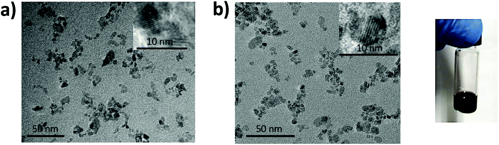 | ||
| Fig. 1 TEM images of non-stoichiometric (a) pristine NiOx and (b) Cu–NiOx(12.2%) NPs with a scale bar of 50 nm. | ||
X-Ray Diffraction (XRD) measurements were performed to explore the crystal structure of both pristine and Cu-doped NiOx NPs. XRD diffractograms are shown in Fig. 2a. The diffraction peaks of the pristine NiOx NPs revealed a cubic crystal structure with three prominent characteristic diffraction peaks at 37.29°, 43.34° and 62.91°, which could be assigned to (111), (200) and (220) planes of NiOx, respectively. Meanwhile, no extra diffraction peaks related to the metallic Cu or copper oxide phase were observed in the XRD diffractogram of Cu-doped NiOx NPs, indicating that doping with Cu did not hardly change the phase structure of NiOx. Furthermore, it could be observed that the diffraction peaks were slightly shifted toward lower angles upon increasing the Cu-doping content. This suggests that the lattice parameter of NiOx was increased upon doping. This was originated from the substitution of Ni ions (ionic radius: 69 pm) with the slightly larger Cu ions (ionic radius: 73 pm).37 The broadening of the diffraction peaks by increasing the content of Cu ions from 2 to 15% could be related to the presence of smaller crystallites since the incorporation of impurities in oxide semiconductors is known to suppress the grain growth and thus result in smaller particles.32 These results are consistent with the TEM results.
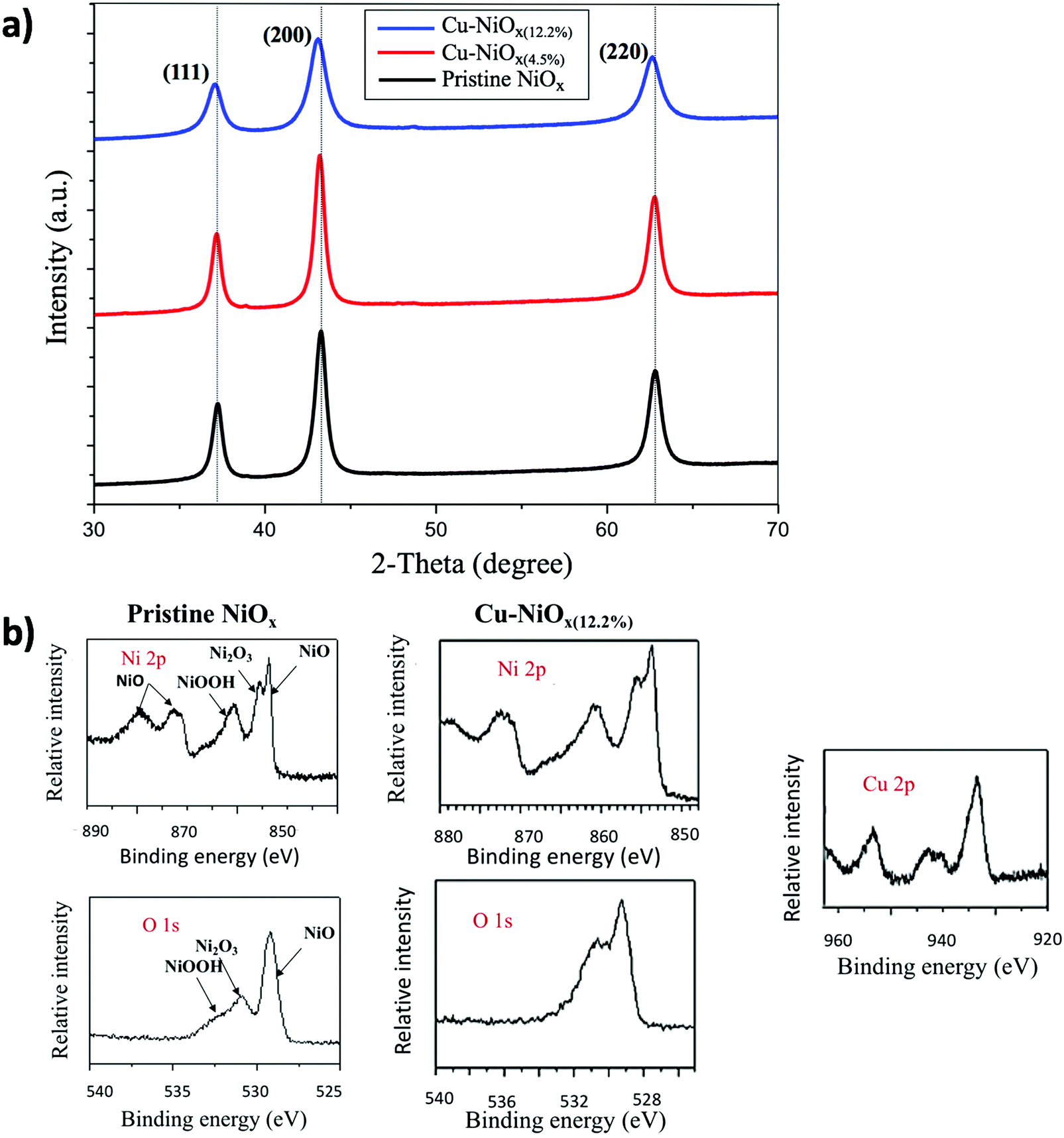 | ||
| Fig. 2 (a) XRD diffractograms and (b) XPS spectra of the pristine and the Cu–NiOx(12.2%) films showing the Ni 2p, O 1s and Cu 2p core level peaks. | ||
Although no crystal phase other than NiOx was detected using XRD, X-Ray Photoelectron Spectroscopy (XPS) measurements were done to demonstrate the effective doping of the NiOx NPs with Cu and to investigate the chemical components of the pristine and the doped NiOx films. The XPS spectra for the pristine NiOx films are shown in Fig. 2b. The Ni 2p3/2 level at 860 eV and the O 1s level at 532.2 eV correspond to the Ni3+ state of the NiOOH species. The Ni 2p3/2 level at 855 eV and the O 1s level at 531 eV peaks can be assigned to the Ni3+ state of Ni2O3. In addition, the presence of the Ni2+ state of NiOx is revealed by the Ni 2p3/2 level at 853.6 eV and the O 1s level at 529 eV peaks as well as the Ni 2p1/2 peak and its satellites at 873.6 and 878.5 eV. These results are consistent with the XPS measurements of the previously synthesized NiOx NPs by Jiang et al.18 The coexistence of Ni2+ and Ni3+ states is a confirmation of the non-stoichiometric nature of NiOx. The XPS spectra of the Cu–NiOx(12.2%) films proved that Cu atoms have been successfully incorporated into the NiOx NPs due to the presence of two peaks located at 933.3 and 953.5 eV corresponding to Cu 2p3/2 and Cu 2p1/2 levels, respectively. These peaks revealed that Cu2+ ions substituted the Ni atom in the NiOx crystal lattice.32
The ultraviolet-visible (UV-vis) absorption spectra of the NiOx solutions were primarily used to find any possible modification in the energy band structure upon doping. As can be observed in Fig. S1 (ESI†), the absorption edge was red-shifted to the visible region upon Cu-doping. This indicates the narrowing of the optical band gap. The band gap of the pristine NiOx as determined from the Tauc plot (3.74 eV) is in good agreement with the reported band gaps.32 By increasing the Cu-doping level, the band gap was decreased to 3.65, 3.6 and 3.56 eV for Cu–NiOx(2.4%), Cu–NiOx(12.2%) and Cu–NiOx(28.2%), respectively. It was reported that the particle size in the metal oxide systems may affect the electronic properties (such as the band gap) of the NPs due to the quantum confinement effect. However, it was also proven that not only quantum confinement can affect the electronic structure, but also doping can have an impact by introducing defect centers into the lattice. These defects can interact with the host lattice to alter the band structure and cause large changes in the electronic properties.38 This phenomenon proved again that Cu was successfully included into the NiOx NPs.
2.2 Solution-processing of NiOx nanocrystals (NCs)
It is known that water-based NiOx solutions can be easily deposited on top of ITO substrates. However, it is not possible to directly deposit such aqueous solutions on top of photoactive layers in PSCs. As seen in the AFM image of Fig. 3a, the deposition of Cu–NiOx(12.2%) solution on top of the PTB7:PC70BM photoactive layer resulted in a bad morphology due to the poor wettability of the water-based solutions on the hydrophobic organic blend. This effect is similar to the case of water-based PEDOT:PSS solutions. Normally, wetting agents such as 2,5,8,11-tetramethyl-6-dodecyn-5,8-diolethoxylate (Dynol 604), Zonyl FS300 fluorosurfactant (Zonyl)40 or Triton-X41 can be added to the PEDOT:PSS water-based solution to decrease the surface tension, thus improving the wettability on top of photoactive layers. However, such additives showed no effect with the synthesized NiOx NPs. Therefore, we followed another strategy to transfer the NiOx dispersion from water into isopropanol by using probe ultrasonication in a mixture of water, isopropanol and methoxy acetic acid surfactant that stabilizes the Cu–NiOx NPs when transferred into IPA solution. The use of this intermediate step allows producing monodispersed cluster-free IPA-based NiOx solutions. Dynamic Light Scattering (DLS) measurements show that the size of the aggregate inside the isopropanol-based solutions corresponds to the size of single NC as determined by TEM.
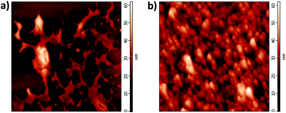 | ||
| Fig. 3 AFM images of (a) water-based Cu–NiOx(12.2%) and (b) IPA-based Cu–NiOx(12.2%) films deposited on top of the PTB7:PC70BM layer. | ||
Additionally, we found that the doping level of the Cu–NiOx NPs impacts the dispersion of the nanoparticles in IPA. Indeed, the highest solubility and most stable solution in IPA were found for 12.2% of Cu-doping, while pristine NiOx or NPs with other doping levels showed lower stability. Importantly, the Cu–NiOx(12.2%) IPA-based solutions were stable for more than six months without the occurrence of any NC aggregation, as confirmed by regular DLS measurements, unlike the aqueous-based solutions having stability not exceeding a few days as can be seen in Fig. S2 (ESI†).
Transmission spectra of the cast NiOx films as a function of Cu-doping levels are shown in Fig. S4 (ESI†). The 40 nm-thick pristine NiOx films revealed a high transmission (>80%) in the visible region. As expected, the optical transmittance was slightly decreased with the increase of the Cu-doping level. This is attributed to the presence of defect states that are responsible for additional absorption, thus lowering the transmittance as seen before for the doped TiO2 NPs.43 Despite this decrease in transmittance due to Cu-doping, the Cu–NiOx(12.2%) layers still present a percentage of transmittance higher than 78% in the visible region. This allows them to function as efficient semi-transparent interfacial layers in polymer solar cells.
2.3 Solar cell devices using Cu–NiOx HTLs
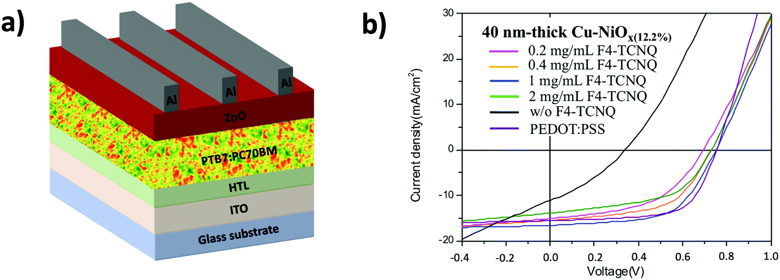 | ||
| Fig. 4 (a) The architecture of the studied regular device structure and (b) typical J–V curves of the PTB7:PC70BM-based devices using different HTLs. | ||
The UPS measurements of the Cu–NiOx(12.2%) layers with and without F4-TCNQ are shown in Fig. S5 (ESI†). The WF was increased from 4.94 eV to 5.45 eV by increasing the F4-TCNQ concentration from 0.2 to 2 mg mL−1, similarly to the NiOx:F4-TCNQ nanocomposite reported by Cheng et al.16 Consequently, solar cells using a 40 nm-thick Cu–NiOx(12.2%) layer with different F4-TCNQ concentrations from 0.2 to 1 mg mL−1 were processed in order to study the impact of the WF tuning on the photovoltaic parameters of the devices. The J–V curves of the devices are shown in Fig. 4b and the photovoltaic parameters are summarized in Table 1. An optimal performance was found for 1 mg mL−1 F4-TCNQ leading to a PCE of 7.4%, a FF of 60%, a VOC of 751 mV and a JSC of 16.6 mA cm−2. This is comparable to that obtained using PEDOT:PSS HTLs with a PCE of 7.6%. A further increase in the F4-TCNQ concentration causes a drop in VOC and FF. These losses could be related to the high WF (5.45 eV) as well as the potential additional resistances generated by the F4-TCNQ layer. We also studied the impact of the HTL thickness on the device performance. The optimized Cu–NiOx(12.2%) thickness was found at 40 nm, as thinner layers of 15 nm showed less compact layer morphology, while a further increase in the HTL thickness caused a decrease in efficiency mainly due to a drop in JSC (see Fig. S6, ESI†). The latter can be related to the increased absorption of the thicker Cu–NiOx HTLs.
| [F4-TCNQ] (mg mL−1) | V OC (mV) | J SC (mA cm−2) | FF (%) | PCE (%) |
|---|---|---|---|---|
| w/o | 340 | 11.05 | 33 | 1.2 |
| 0.2 | 693 | 15 | 50 | 5.2 |
| 0.4 | 730 | 15.5 | 55.2 | 6.2 |
| 1 | 751 | 16.6 | 60 | 7.4 |
| 2 | 729 | 13.9 | 53 | 5.3 |
| PEDOT:PSS | 752 | 15.5 | 65 | 7.6 |
In this regard, we focused our studies on the inverted device structures using PBDB-T-2F:IT-4F photoactive layers. The studied device architecture is ITO/ZnO/80 nm-thick PBDB-T-2F:IT-4F/HTL/Ag as shown in Fig. 5a. The J–V curves of the corresponding devices are presented in Fig. 5b and the photovoltaic parameters are summarized in Table 2. As a reference cell, an efficiency of 11% was obtained using a 2 nm-thick evaporated MoO3 HTL with a 62% FF after post-annealing the whole device at 100 °C for 10 minutes. By replacing the evaporated HTL with a 40 nm-thick molecularly doped Cu–NiOx(12.2%) HTL, the optimized efficiency obtained was 7.92% with a FF of 53.3%, a VOC of 827 mV and a JSC of 18 mA cm−2. The lower PCE, compared to the reference cells using MoOx, is due to losses in all photovoltaic parameters indicating that the HTL is not yet fully optimized for NFA-based solar cells.
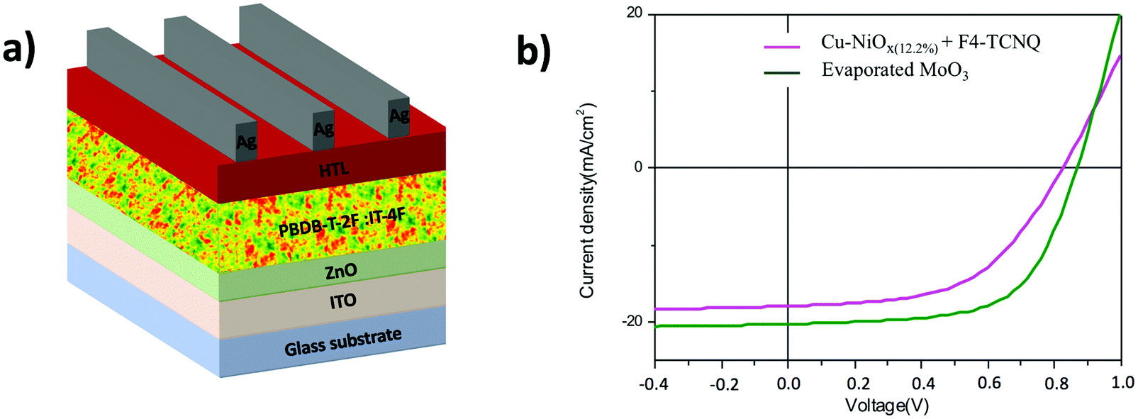 | ||
| Fig. 5 (a) The architecture of the studied inverted device structure and (b) the J–V curves of the PBDB-T-2F:IT-4F-based inverted device structures using different HTLs. | ||
| HTL | V OC (mV) | J SC (mA cm−2) | FF (%) | PCE (%) |
|---|---|---|---|---|
| 2 nm e-MoO3 | 871 | 20.3 | 62 | 11 |
| 40 nm Cu–NiOx(12.2%) + F4-TCNQ | 827 | 18 | 53.3 | 7.92 |
| 40 nm modified PEDOT:PSS | 700 | 19 | 46.3 | 6.3 |
The decrease in VOC and FF indicates still residual misalignment of the interface levels leading to barriers for hole extraction. For comparison, we also processed devices using modified PEDOT:PSS inks with suitable wettability properties for processing on top of the polymer blend. These inks have been previously optimized for fullerene-based blends. As can be seen in Fig. S7 (ESI†) and Table 2, these devices show clearly lower performances compared to the devices processed with the hybrid HTLs. Indeed, even stronger losses in VOC and FF are found for PEDOT:PSS-based devices, indicating the occurrence of strong interfacial losses compared to cells using fullerene acceptors. While the performance losses in VOC and FF need further improvement in the electronic properties of the hybrid HTL, we focus in the following paragraph on the losses in JSC that may be related to optical spacer effects.
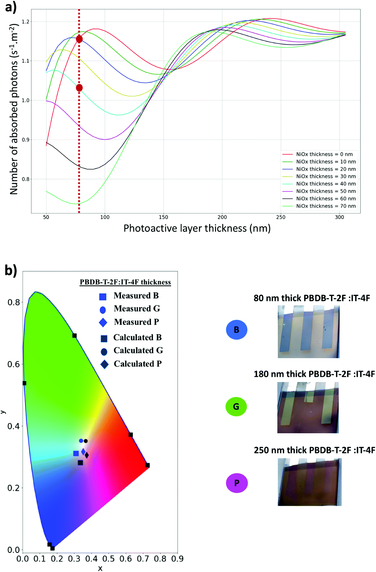 | ||
| Fig. 6 (a) The theoretical total number of photons absorbed inside the PBDB-T-2F:IT-4F photoactive layer as a function of photoactive layer thickness for different Cu–NiOx(12.2%) thicknesses. (b) Measured (blue dots) and calculated (grey dots) color coordinates for the three experimental blue, green and pink solar cells (left) and photographic images of the corresponding cells (right). | ||
The first maximum corresponds to blend thickness ranging from 50 to 90 nm with the exact position of each maximum depending on the Cu–NiOx layer thickness. The second maximum is broader with photoactive layer thickness ranging from 170 to 250 nm. These simulations reveal that, for thin photoactive layers, the Cu–NiOx-based HTLs always lead to a reduction of light absorption inside the active layer compared to solar cells processed without any HTL. In contrast, using thick blend layers, light absorption is almost unchanged as long as the HTL is not surpassing the 40–50 nm range. This finding is identical to the case of solar cells using the regular device structures with ZnO or aluminum-doped ZnO as optical spacers.35,42 Here, the solar cells using the Cu–NiOx(12.2%) HTL have 80 nm-thick photoactive layers that were optimized for the ultrathin MoO3 HTLs. This is comparable to the situation of the red curve in Fig. 6a, considering that devices using a 2 nm-thick MoO3 have almost equivalent absorption to those processed without any HTL. The use of a 40 nm-thick Cu–NiOx(12.2%) HTL reduced strongly the amount of absorbed light in the photoactive layer by approximately 10–15%, as shown by the vertical red dotted line as a guide to the eye. By considering these calculations, we indeed find the corresponding losses in JSC for the devices fabricated with Cu–NiOx(12.2%) (18 mA cm−2) when compared to the reference cells fabricated with MoO3 generating 20.3 mA cm−2. These calculations also allow us to discuss the most suitable conditions for the developed Cu–NiOx(12.2%):F4-TCNQ bilayers used in inverted device structures. By considering a 40 nm-thick Cu–NiOx(12.2%) HTL, the photoactive layer should be at least 180 nm in order to limit the optical losses.
As it was shown recently, the use of optical spacers also allows modifying the color of polymer solar cells.35 Indeed, the HTLs not only modify the amount of light absorbed inside the active layer but also determine the light reflection of the solar cell, thus affecting the color of the devices. To estimate the potential of the Cu–NiOx optical spacers in generating colored polymer solar cells, we calculated the color coordinates of the devices in the reflection mode as a function of the photoactive layer and Cu–NiOx thickness. Thus, for a 40 nm-thick Cu–NiOx(12.2%) HTL, the color coordinates corresponding to the reflected light were calculated for photoactive layer thickness ranging between 80 and 250 nm. Fig. 6b is a chromaticity diagram showing a comparison between the calculated and the measured color coordinates of three different solar cells (B, G and P) with different blend thicknesses (80, 180 and 250 nm, respectively). One can first notice that, as expected, the color of the devices can be strongly tuned by adjusting the photoactive layer thickness, thus comparable to the case of solar cells elaborated in regular device structure having ZnO electron transport layers. For an 80 nm-thick photoactive layer, the devices have a blue color. They become successively green and pink when the active layer thickness is increased to 180 and 250 nm, respectively. Importantly, very good agreements were found between the color coordinates obtained from simulations with the different measured colors of the three solar cells. Thus, these results show that a large palette of colors can be produced with this technique, making fine-tuning of the color possible via adjusting the Cu–NiOx optical spacer and the photoactive layer thickness, owing to the control in the light absorption amount.
3. Conclusion
Nickel oxide nanoparticles in alcoholic solutions were developed in this work for processing hole transport layers and were applied to non-fullerene acceptor-based solar cells using inverted device structures. We show that copper doping of NiOx nanoparticles is beneficial to reach aggregate-free solution suitable for processing the HTL on top of photoactive layers. Further doping of these nanoparticles with the organic electron acceptor F4-TCNQ was necessary to optimize the work function of the HTL for efficient hole extraction. Solar cells using normal device structures revealed that such hybrid HTL can be processed up to 45 nm without inducing electric losses due to optimized work function and high conductivity. Processing the hybrid HTLs on top of polymer blends based on IT-4F and PBDB-T-2F led to solar cells with promising efficiencies up to 7.9%, while further work function optimization is needed to reach fully optimized solution-processed organic–inorganic Cu–NiOx nanoparticles for NFA-based solar cells using inverted device structures. We also demonstrated for the first time that the use of the hybrid HTL in the inverted device structure of polymer solar cells allows for color tuning over a large palette using optical spacer effects. Our future work will focus on the optimization of the work function and transport properties of the organic–inorganic doped NiOx HTL by combining 2D-materials such as graphene oxide to generate highly efficient HTLs for fully solution-processed solar cells using NFAs with improved air stability.4. Experimental section
4.1 Synthesis of highly soluble NiOx NPs
All the materials were purchased from Sigma Aldrich unless specified elsewhere. NiOx NPs were prepared by a chemical precipitation method according to a previous report.18 Typically, 0.05 mole of Ni(NO3)2·6H2O was dispersed in 100 mL of deionized water. A dark green solution was obtained. Under continuous magnetic stirring, the pH of the solution was adjusted to 10 by dropwise addition of 10 M NaOH aqueous solution. The pH value was measured using a pH meter (Hanna HI 8417 pH meter). After stirring for 10 minutes, the green colloidal precipitate was washed twice with deionized water using centrifugation and dried at 80 °C overnight. To ensure complete calcination, the obtained green solid was ground to a fine powder using a pestle and a mortar, then calcined at 270 °C for 2 hours to yield a black powder. For the Cu–NiOx NPs, the same procedure was followed. The only difference is the addition of the Cu(NO3)2·xH2O precursor in the initial solution at various molar ratios (from 2 to 20%).4.2 Preparation of the NiOx solutions
NiOx NPs were dispersed in water to the desired concentration. Then, the solution was transferred to IPA solvent and dispersed by probe ultrasonication until obtaining an aggregate-free solution.4.3 Preparation of the ZnO solutions
ZnO NPs were prepared as published elsewhere.46,47 The cluster-free ZnO nanoparticle solution of 5 mg mL−1 was prepared by transferring the as-synthesized ZnO nanoparticles from methanol into isopropanol mixed with ethanolamine (0.2 vol%).4.4 Characterization methods
The NiOx NCs were characterized by HR-TEM (JEOL 3010, acceleration voltage of 300 kV). The samples were prepared by drop-casting a diluted isopropanol solution of NiOx NCs onto a carbon-coated copper grid. UV-vis absorption of the NiOx NCs in solution and on films was recorded using a Varian CARY 50 spectrophotometer. Size distribution of the NCs within the solution was determined by DLS using a Nano ZetaSizer from Malvern. The crystallinity of the NiOx NCs was measured by XRD using an INEL with a linear detector. AFM was realized using a NTEGRA Prima of the brand NT-MDT in tapping mode to study the quality of the NiOx NCs layers. The layer thickness was determined using a mechanical profilometer. Photoemission spectroscopy using UV (UPS, HeI 21.2 eV) and X-ray (XPS, monochromatized Al Kα 1486.7 eV) light sources was performed at Linkoping University in Sweden.4.5 Optical simulations of the solar cells
Ellipsometry was used to extract the optical indices of Cu–NiOx thin films. The measurements were performed for wavelengths ranging between 380 and 1000 nm using a Semilab rotating compensator ellipsometer equipped with a microspot which focuses the beam on a very small area of the sample (a circle with a diameter of 100 μm).The layers were coated on glass substrates. SEA software (Semilab company) was used to fit the SE measurements of tan(Ψ) and cos(Δ) and extract the optical indices n(λ) and k(λ) of the materials. The dielectric functions ε = ε1 + i × ε2 of PBDB-T-2F:IT-4F were fitted with the Gaussian model that is adequate for the parameterization of the optical functions of amorphous thin films in the interband region.48 The dielectric functions of Cu–NiOx(12.2%) were fitted with a Gauss–Sellmeyer model in order to take into account both the dielectric and the absorbing character of this material. The optical indices of PBDB-T-2F:IT-4F and Cu–NiOx(12.2%) are shown in Fig. S8 (ESI†). On the other hand, the optical indices of ITO, ZnO and Ag were taken from the literature.42,44 The CIE xyY (1931) model was employed for the color prediction of the polymer solar cells. This model allows calculating the normalized color coordinates (x, y) of solar cells from their reflection spectra by considering the human eye sensitivity. Using the optical indices of the materials as input parameters, the reflection spectra of the solar cells were calculated using a transfer matrix method.45 The reflection spectra of the cells were measured using a PerkinElmer spectrophotometer Lambda 950.
4.6 Solar cell fabrication
The organic-BHJ solar cells were prepared following several steps. First, the ITO substrates (15 Ω sq−1) were cleaned by using deionized water, acetone, ethanol, and isopropanol with ultrasonication. Then, the pre-cleaned ITO substrates were exposed to UV-ozone treatment for 15 min to reform the surface. In the case of regular device structures, a thin layer of PEDOT:PSS (Heraeus, CLEVIOS PVP AI 4083) was spin-coated on the pre-cleaned ITO substrates at a speed of 3500 rpm for 60 s followed by heating on a hotplate at 140 °C for 20 min to obtain a film thickness of ≈40 nm. The NiOx HTLs were spin-coated at 2500 rpm for 60 s from solutions of different concentrations (10 to 30 mg mL−1) to obtain different film thicknesses. These NiOx films were then annealed on a hot plate in air at 80 °C for 10 min. A solution of F4-TCNQ (Ossilla) with different concentrations (from 0.2 to 2 mg mL−1) was spin-coated with the same speed and annealed at 80 °C for 30 min. The substrates were then transferred into a nitrogen-filled glovebox. The PTB7:PC70BM blend solution was prepared from a weight ratio of 1![[thin space (1/6-em)]](https://www.rsc.org/images/entities/char_2009.gif) :1.5 and a total concentration of 25 mg mL−1 in chlorobenzene with 0.3 vol% 1,8-diiodooctane processing additive. After stirring overnight at 60 °C, the BHJ thin films (90 nm) were obtained from spin-coating the solution at 1800 rpm for 120 s. The active layers were then subjected to high vacuum overnight. ZnO NCs were processed by spin-coating a 5 mg mL−1 solution on top of the active layers at 1500 rpm for 60 s followed by annealing for 2 min at 80 °C. The top Al metal electrode (100 nm) was thermally evaporated at 1 × 10⁻⁶ Torr pressure through a shadow mask with a device area of 0.27 cm2.
:1.5 and a total concentration of 25 mg mL−1 in chlorobenzene with 0.3 vol% 1,8-diiodooctane processing additive. After stirring overnight at 60 °C, the BHJ thin films (90 nm) were obtained from spin-coating the solution at 1800 rpm for 120 s. The active layers were then subjected to high vacuum overnight. ZnO NCs were processed by spin-coating a 5 mg mL−1 solution on top of the active layers at 1500 rpm for 60 s followed by annealing for 2 min at 80 °C. The top Al metal electrode (100 nm) was thermally evaporated at 1 × 10⁻⁶ Torr pressure through a shadow mask with a device area of 0.27 cm2.
For the inverted device structures, 1 wt% ZnO (Avantama) was spin-coated on top of the pre-cleaned ITO substrates at 5000 rpm for 60 s and then annealed at 120 °C for 10 min in air. The PBDB-T-2F:IT-4F solution was prepared from a weight ratio of 1:1 and a total concentration of 20 mg mL−1 in o-xylene. After stirring overnight at room temperature, the active layers were prepared by spin-casting the ink at 2200 rpm for 2 min (without annealing). A 2 nm-thick MoO3 layer and a 100 nm-thick silver layer were then thermally evaporated onto the surface of the active layer at 2 × 10⁻⁶ Torr pressure through a shadow mask. For each device configuration, a total of six cells were measured. The current density–voltage (J–V) characteristics of the devices were measured using a Keithley 238 Source Measure Unit. Solar cell performance was measured using a Newport classe AAA 1.5 Global solar simulator (Oriel Sol3ATM model no. 94043A) with an irradiation intensity of 100 mW cm−2. The light intensity was determined with a Si reference cell (Newport Company, Oriel no. 94043A) calibrated by National Renewable Energy Laboratory (NREL).
Conflicts of interest
There are no conflicts to declare.Acknowledgements
The authors thank Alain Ranguis, Damien Chaudanson and Vasile Heresanu from CINaM laboratory for their assistance in the use of AFM, TEM and XRD facilities. They also acknowledge Igor Ozerov and Frédéric Bedu for the profilometer measurements performed at the PLANETE CT PACA cleanroom facility. RA thanks the french Ministère de l'Enseignement Supérieur, de la Recherche et de l'Innovation for Ph.D. grant funding.References
- Q. Liu, Y. Jiang, K. Jin, J. Qin, J. Xu, W. Li, J. Xiong, J. Liu, Z. Xiao, K. Sun, S. Yang, X. Zhang and L. Ding, 18% Efficiency organic solar cells, Sci. Bull., 2020, 65, 272–275 CrossRef CAS.
- R. Po, C. Carbonera, A. Bernardi and N. Camaioni, The role of buffer layers in polymer solar cells, Energy Environ. Sci., 2011, 4, 285–310 RSC.
- A. N. Bartynski, C. Trinh, A. Panda, K. Bergemann, B. E. Lassiter, J. D. Zimmerman, S. R. Forrest and M. E. Thompson, A Fullerene-Based Organic Exciton Blocking Layer with High Electron Conductivity, Nano Lett., 2013, 13, 3315–3320 CrossRef CAS.
- M. C. Scharber, D. Mühlbacher, M. Koppe, P. Denk, C. Waldauf, A. J. Heeger and C. J. Brabec, Design Rules for Donors in Bulk-Heterojunction Cells—Towards 10% Energy-Conversion Efficiency, Adv. Mater., 2006, 18, 789–794 CrossRef CAS.
- Y. Xia, K. Sun and J. Ouyang, Solution-Processed Metallic Conducting Polymer Films as Transparent Electrode of Optoelectronic Devices, Adv. Mater., 2012, 24, 2436–2440 CrossRef CAS.
- Q. Li, J. Yang, S. Chen, J. Zou, W. Xie and X. Zeng, Highly Conductive PEDOT:PSS Transparent Hole Transporting Layer with Solvent Treatment for High Performance Silicon/Organic Hybrid Solar Cells, Nanoscale Res. Lett., 2017, 12, 506 CrossRef.
- Y. Meng, Z. Hu, N. Ai, Z. Jiang, J. Wang, J. Peng and Y. Cao, Improving the Stability of Bulk Heterojunction Solar Cells by Incorporating pH-Neutral PEDOT:PSS as the Hole Transport Layer, ACS Appl. Mater. Interfaces, 2014, 6, 5122–5129 CrossRef CAS.
- W.-H. Baek, M. Choi, T.-S. Yoon, H. H. Lee and Y.-S. Kim, Use of fluorine-doped tin oxide instead of indium tin oxide in highly efficient air-fabricated inverted polymer solar cells, Appl. Phys. Lett., 2010, 96, 133506 CrossRef.
- Y.-J. Cheng, C.-H. Hsieh, Y. He, C.-S. Hsu and Y. Li, Combination of Indene-C60 Bis-Adduct and Cross-Linked Fullerene Interlayer Leading to Highly Efficient Inverted Polymer Solar Cells, J. Am. Chem. Soc., 2010, 132, 17381–17383 CrossRef CAS.
- S. K. Hau, H.-L. Yip, H. Ma and A. K.-Y. Jen, High performance ambient processed inverted polymer solar cells through interfacial modification with a fullerene self-assembled monolayer, Appl. Phys. Lett., 2008, 93, 233304 CrossRef.
- F. Wang, Z. Tan and Y. Li, Solution-processable metal oxides/chelates as electrode buffer layers for efficient and stable polymer solar cells, Energy Environ. Sci., 2015, 8, 1059–1091 RSC.
- D. Ouyang, Z. Huang and W. C. H. Choy, Solution-Processed Metal Oxide Nanocrystals as Carrier Transport Layers in Organic and Perovskite Solar Cells, Adv. Funct. Mater., 2019, 29, 1804660 CrossRef.
- D. Ouyang, J. Xiao, F. Ye, Z. Huang, H. Zhang, L. Zhu, J. Cheng and W. C. H. Choy, Strategic Synthesis of Ultrasmall NiCo2O4 NPs as Hole Transport Layer for Highly Efficient Perovskite Solar Cells, Adv. Energy Mater., 2018, 8, 1702722 CrossRef.
- B. Yang, D. Ouyang, Z. Huang, X. Ren, H. Zhang and W. C. H. Choy, Multifunctional Synthesis Approach of In:CuCrO2 Nanoparticles for Hole Transport Layer in High-Performance Perovskite Solar Cells, Adv. Funct. Mater., 2019, 29, 1902600 CrossRef.
- Z. Huang, D. Ouyang, R. Ma, W. Wu, V. A. L. Roy and W. C. H. Choy, A General Method: Designing a Hypocrystalline Hydroxide Intermediate to Achieve Ultrasmall and Well-Dispersed Ternary Metal Oxide for Efficient Photovoltaic Devices, Adv. Funct. Mater., 2019, 29, 1904684 CrossRef CAS.
- J. Cheng, X. Ren, H. L. Zhu, J. Mao, C. Liang, J. Zhuang, V. A. L. Roy and W. C. H. Choy, Pre- and post-treatments free nanocomposite based hole transport layer for high performance organic solar cells with considerably enhanced reproducibility, Nano Energy, 2017, 34, 76–85 CrossRef CAS.
- Z. Huang, G. Natu, Z. Ji, M. He, M. Yu and Y. Wu, Probing the Low Fill Factor of NiO p-Type Dye-Sensitized Solar Cells, J. Phys. Chem. C, 2012, 116, 26239–26246 CrossRef CAS.
- F. Jiang, W. C. H. Choy, X. Li, D. Zhang and J. Cheng, Post-treatment-Free Solution-Processed Non-stoichiometric NiO(x) Nanoparticles for Efficient Hole-Transport Layers of Organic Optoelectronic Devices, Adv. Mater., 2015, 27, 2930–2937 CrossRef CAS.
- M. D. Irwin, D. B. Buchholz, A. W. Hains, R. P. H. Chang and T. J. Marks, p-Type semiconducting nickel oxide as an efficiency-enhancing anode interfacial layer in polymer bulk-heterojunction solar cells, Proc. Natl. Acad. Sci. U. S. A., 2008, 105, 2783–2787 CrossRef CAS.
- S.-Y. Park, H.-R. Kim, Y.-J. Kang, D.-H. Kim and J.-W. Kang, Organic solar cells employing magnetron sputtered p-type nickel oxide thin film as the anode buffer layer, Sol. Energy Mater. Sol. Cells, 2010, 94, 2332–2336 CrossRef CAS.
- Z. Yi Wang, S.-H. Lee, D.-H. Kim, J.-H. Kim and J.-G. Park, Effect of NiOx thin layer fabricated by oxygen-plasma treatment on polymer photovoltaic cell, Sol. Energy Mater. Sol. Cells, 2010, 94, 1591–1596 CrossRef.
- S. Seo, I. J. Park, M. Kim, S. Lee, C. Bae, H. S. Jung, N.-G. Park, J. Y. Kim and H. Shin, An ultra-thin, un-doped NiO hole transporting layer of highly efficient (16.4%) organicntingancti hybrid perovskite solar cells, Nanoscale, 2016, 8, 11403–11412 RSC.
- A. Garcia, G. C. Welch, E. L. Ratcliff, D. S. Ginley, G. C. Bazan and D. C. Olson, Improvement of Interfacial Contacts for New Small-Molecule Bulk-Heterojunction Organic Photovoltaics, Adv. Mater., 2012, 24, 5368–5373 CrossRef CAS.
- S. Yoon and D.-W. Kang, Solution-processed nickel oxide hole transport layer for highly efficient perovskite-based photovoltaics, Ceram. Int., 2018, 44, 9347–9352 CrossRef CAS.
- K. Zilberberg, J. Meyer and T. Riedl, Solution processed metal-oxides for organic electronic devices, J. Mater. Chem. C, 2013, 1, 4796–4815 RSC.
- H. Zhang, J. Cheng, D. Li, F. Lin, J. Mao, C. Liang, A. K.-Y. Jen, M. Grätzel and W. C. H. Choy, Toward All Room-Temperature, Solution-Processed, High-Performance Planar Perovskite Solar Cells: A New Scheme of Pyridine-Promoted Perovskite Formation, Adv. Mater., 2017, 29, 1604695 CrossRef.
- X. Yin, P. Chen, M. Que, Y. Xing, W. Que, C. Niu and J. Shao, Highly Efficient Flexible Perovskite Solar Cells Using Solution-Derived NiOx Hole Contacts, ACS Nano, 2016, 10, 3630–3636 CrossRef CAS.
- J. Ciro, D. Ramoact, M. A. Mejoa Escobar, J. F. Montoya, S. Mesa, R. Betancur and F. Jaramillo, Self-Functionalization Behind a Solution-Processed NiOx Film Used As Hole Transporting Layer for Efficient Perovskite Solar Cells, ACS Appl. Mater. Interfaces, 2017, 9, 12348–12354 CrossRef CAS.
- H. Zhang, J. Cheng, F. Lin, H. He, J. Mao, K. S. Wong, A. K.-Y. Jen and W. C. H. Choy, Pinhole-Free and Surface-Nanostructured NiOx Film by Room-Temperature Solution Process for High-Performance Flexible Perovskite Solar Cells with Good Stability and Reproducibility, ACS Nano, 2016, 10, 1503–1511 CrossRef CAS.
- J. Cheng, H. Zhang, Y. Zhao, J. Mao, C. Li, S. Zhang, K. S. Wong, J. Hou and W. C. H. Choy, Self-Assembled Quasi-3D Nanocomposite: A Novel p-Type Hole Transport Layer for High Performance Inverted Organic Solar Cells, Adv. Funct. Mater., 2018, 28, 1706403 CrossRef.
- J. W. Jung, C.-C. Chueh and A. K.-Y. Jen, A Low-Temperature, Solution-Processable, Cu-Doped Nickel Oxide Hole-Transporting Layer via the Combustion Method for High-Performance Thin-Film Perovskite Solar Cells, Adv. Mater., 2015, 27, 7874–7880 CrossRef CAS.
- Q. He, K. Yao, X. Wang, X. Xia, S. Leng and F. Li, Room-Temperature and Solution-Processable Cu-Doped Nickel Oxide Nanoparticles for Efficient Hole-Transport Layers of Flexible Large-Area Perovskite Solar Cells, ACS Appl. Mater. Interfaces, 2017, 9, 41887–41897 CrossRef CAS.
- J.-Y. Jeng, M.-W. Lin, Y.-J. Hsu, T.-C. Wen and T.-F. Guo, The Roles of Poly(Ethylene Oxide) Electrode Buffers in Efficient Polymer Photovoltaics, Adv. Energy Mater., 2011, 1, 1192–1198 CrossRef CAS.
- F. Guillain, J. Endres, L. Bourgeois, A. Kahn, L. Vignau and G. Wantz, Solution-Processed p-Dopant as Interlayer in Polymer Solar Cells, ACS Appl. Mater. Interfaces, 2016, 8, 9262–9267 CrossRef CAS.
- M. Gaceur, S. B. Dkhil, D. Duchl, F. Bencheikh, J.-J. Simon, L. Escoubas, M. Mansour, A. Guerrero, G. Garcia-Belmonte, X. Liu, M. Fahlman, W. Dachraoui, A. K. Diallo, C. Videlot-Ackermann, O. Margeat and J. Ackermann, Ligand-Free Synthesis of Aluminum-Doped Zinc Oxide Nanocrystals and their Use as Optical Spacers in Color-Tuned Highly Efficient Organic Solar Cells, Adv. Funct. Mater., 2016, 26, 243–253 CrossRef CAS.
- A. K. K. Kyaw, D. H. Wang, D. Wynands, J. Zhang, T.-Q. Nguyen, G. C. Bazan and A. J. Heeger, Improved Light Harvesting and Improved Efficiency by Insertion of an Optical Spacer (ZnO) in Solution-Processed Small-Molecule Solar Cells, Nano Lett., 2013, 13, 3796–3801 CrossRef CAS.
- R. D. Shannon, Revised effective ionic radii and systematic studies of interatomic distances in halides and chalcogenides, Acta Crystallogr., Sect. A: Cryst. Phys., Diffr., Theor. Gen. Crystallogr., 1976, 32, 751–767 CrossRef.
- M. Singh, M. Goyal and K. Devlal, Size and shape effects on the band gap of semiconductor compound nanomaterials, J. Taibah Univ. Sci., 2018, 12, 470–475 CrossRef.
- T. N. Ramesh and P. V. Kamath, Synthesis of nickel hydroxide: effect of precipitation conditions on phase selectivity and structural disorder, J. Power Sources, 2006, 156, 655–661 CrossRef CAS.
- A. Savva, M. Neophytou, C. Koutsides, K. Kalli and S. A. Choulis, Synergistic effects of buffer layer processing additives for enhanced hole carrier selectivity in inverted Organic Photovoltaics, Org. Electron., 2013, 14, 3123–3130 CrossRef CAS.
- M. Wagner, C. D. O’Connell, D. G. Harman, R. Sullivan, A. Ivaska, M. J. Higgins and G. G. Wallace, Synthesis and optimization of PEDOT:PSS based ink for printing nanoarrays using Dip-Pen Nanolithography, Synth. Met., 2013, 181, 64–71 CrossRef CAS.
- S. B. Dkhil, D. Duchl, M. Gaceur, A. K. Thakur, F. B. Aboura, L. Escoubas, J.-J. Simon, A. Guerrero, J. Bisquert, G. Garcia-Belmonte, Q. Bao, M. Fahlman, C. Videlot-Ackermann, O. Margeat and J. Ackermann, Interplay of Optical, Morphological, and Electronic Effects of ZnO Optical Spacers in Highly Efficient Polymer Solar Cells, Adv. Energy Mater., 2014, 4, 1400805 CrossRef.
- V. R. Akshay, B. Arun, G. Mandal and M. Vasundhara, Visible range optical absorption, Urbach energy estimation and paramagnetic response in Cr-doped TiO2 nanocrystals derived by a solived method, Phys. Chem. Chem. Phys., 2019, 21, 12991–13004 RSC.
- D. Duch, E. Drouard, J. J. Simon, L. Escoubas, P. Torchio, J. Le Rouzo and S. Vedraine, Light harvesting in organic solar cells, Sol. Energy Mater. Sol. Cells, 2011, 95, S18–S25 CrossRef.
- D. Duchs, F. Bencheikh, S. B. Dkhil, M. Gaceur, N. Berton, O. Margeat, J. Ackermann, J. J. Simon and L. Escoubas, Optical performance and color investigations of hybrid solar cells based on P3HT:ZnO, PCPDTBT:ZnO, PTB7:ZnO and DTS(PTTh2)2:ZnO, Sol. Energy Mater. Sol. Cells, 2014, 126, 197–204 CrossRef.
- G. E. Jellison and F. A. Modine, Parameterization of the optical functions of amorphous materials in the interband region, Appl. Phys. Lett., 1996, 69, 371–373 CrossRef CAS.
- G. Mattioli, S. B. Dkhil, M. I. Saba, G. Malloci, C. Melis, P. Alippi, F. Filippone, P. Giannozzi, A. K. Thakur, M. Gaceur, O. Margeat, A. K. Diallo, C. Videlot-Ackermann, J. Ackermann, A. A. Bonapasta and A. Mattoni, Interfacial Engineering of P3HT/ZnO Hybrid Solar Cells Using Phthalocyanines: A Joint Theoretical and Experimental Investigation, Adv. Energy Mater, 2014, 4, 1301694 CrossRef.
- F. Bencheikh, D. Duchh, C. M. Ruiz, J.-J. Simon and L. Escoubas, Study of Optical Properties and Molecular Aggregation of Conjugated Low Band Gap Copolymers: PTB7 and PTB7-Th, J. Phys. Chem. C, 2015, 119, 24643–24648 CrossRef CAS.
Footnote |
| † Electronic supplementary information (ESI) available. See DOI: 10.1039/d0qm00619j |
| This journal is © the Partner Organisations 2021 |