DOI:
10.1039/D0QM00553C
(Research Article)
Mater. Chem. Front., 2021,
5, 324-332
Ultra-low thermal conductivity and high thermoelectric performance realized in a Cu3SbSe4 based system†
Received
29th July 2020
, Accepted 11th September 2020
First published on 15th September 2020
Abstract
Cu3SbSe4-Based materials were fabricated through Sn-doping and AgSb0.98Ge0.02Se2 incorporation and their thermoelectric properties were investigated in the temperature range from 300 K to 675 K. A remarkable enhancement in thermoelectric performance was obtained, which can be ascribed to the synergistic adjustment of electrical and thermal transport. The introduction of AgSb0.98Ge0.02Se2 nanoparticles strengthened phonon scattering in the composites, resulting in a low thermal conductivity. Simultaneously, a high power factor was maintained. As a result, a maximum figure of merit of 1.23 was obtained at 675 K for the sample Cu3Sb0.96Sn0.04Se4–3 wt% AgSb0.98Ge0.02Se2, which is one of the highest values ever reported in the Cu3SbSe4-based system.
1. Introduction
Energy shortages and environmental degradation have become major issues that have increasingly haunted humanity with the development of industrial society.1 In this context, thermoelectric (TE) materials can be used as solid state refrigerators or heat pumps that can directly convert waste heat from industrial production into electricity and provide possible solutions to address energy shortages.2,3 It is known that the TE energy conversion efficiency is defined by the dimensionless figure-of-merit ZT = S2σT/κ, where S, σ, T and κ are the Seebeck coefficient, electrical conductivity, absolute temperature and thermal conductivity, respectively.4 As one of the novel chalcogenide thermoelectric materials, the ternary cooper-based p-type semiconductor Cu3SbSe4 has attracted more attention due to its relatively low thermal conductivity and comparatively narrow band gap of ∼0.29 eV.5–7 It has two Cu sites with different Cu–Se bond lengths and the Cu–Se framework provides paths for carrier transport with comparatively high mobility. Furthermore, a relatively complex crystal structure hinders the phonon transport effectively, resulting in a comparatively low thermal conductivity. So far, many efforts have been devoted to enhancing the TE performance of Cu3SbSe4, such as optimizing the carrier concentration or enhancing the Seebeck coefficient through doping using solid state reaction or chemical methods.8–10 Tian Zhou et al. carried out research on 3D flower-like hierarchical Ti-doped Cu3SbSe4 microspheres, which possessed an ultra-low thermal conductivity of 0.38 W m−1 K−1 at 623 K and eventually reached the promising ZT value of ∼0.59 at this temperature.11 Boyi Wang et al. developed a synergistic modulation of the thermal conductivity and power factor of Cu3SbSe4 based materials through Sn and Zr or Hf co-doping by using a facile microwave-assisted solvothermal method, yielding a peak ZT value of ∼0.82 for Cu3Sb0.91Sn0.03Hf0.06Se4 at 623 K, which was ∼228% higher than that of pristine Cu3SbSe4.12 Zhang Dan et al. carried out research on weakening p–d hybridization via Ag substitution at the Cu site, wherein the impaired Cu–Se bonding increased the hole concentration and the second phase AgSbSe2 gave rise to large strain fluctuations, which reduced the lattice thermal conductivity remarkably. The peak ZT value of ∼ 0.9 was achieved in the sample Cu2.85Ag0.15SbSe4. Xie Dandan et al. investigated (Ag and Sn) co-doped Cu3SbSe4 nanocrystals using the microwave-assisted solvothermal method. The results demonstrated that Cu2−xSe nanoinclusions served as additional scattering centers for phonons. A maximum ZT of 1.18 at 623 K for Cu2.8Ag0.2Sb0.95Sn0.05Se4 was obtained. We fabricated large-scale nanostructured Sn-doped samples through a low-temperature co-precipitation route and the highest ZT obtained for Cu3Sb0.98Sn0.02Se4 was 1.05.13 As an effective means to enhance the thermoelectric performance, low thermal conductivity was derived from increasing phonon scattering at grain boundaries and nanoparticles by nanostructuring.14,15 In our previous work, second nanoparticles of Cu3Sb0.94Sn0.06Se2.5S1.5 were introduced into the Cu3Sb0.96Sn0.04Se4 matrix and we obtained a minimum κL of about 0.62 W m−1 K−1 for the nanocomposites, which was about a 34% reduction compared with that of the matrix.16 Unfortunately, the introduction of nanoparticles resulted in a decrease of power factor and weakened the thermoelectric performance. Up to now, few effective methods can simultaneously realize a significant enhancement of power factor and reduction of thermal conductivity for the Cu3SbSe4 based system.
In order to further modulate electrical and thermal transport properties, we chose nanoparticles embedded in the Cu3Sb0.96Sn0.04Se4 matrix, introducing scattering centers, through which the power factor can be enhanced and κL can be decreased simultaneously. In this work, AgSb0.98Ge0.02Se2 has been selected as the second nanophase because of its intrinsic low thermal conductivity and high TE performance.17,18 The experimental results demonstrate that the incorporation of AgSb0.98Ge0.02Se2 nanoinclusions in Cu3Sb0.96Sn0.04Se4 results in an enhancement of power factor due to the enhanced carrier mobility. In addition, thermal conductivity is reduced due to the enhanced scattering, which is consistent with our calculation of lattice thermal conductivity. As a result, a 9.5% enhancement of power factor as well as a 57.3% reduction of lattice thermal conductivity is realized in the composite sample with y = 3 wt%. Consequently, a record high ZT of 1.23 (at 675 K) is achieved, which is larger than that of any reported Cu3SbSe4-based materials.
2. Experimental section
Polycrystals of Cu3Sb0.96Sn0.04Se4 were prepared using a melting method. Elementary Cu (99.99%), Sb (99.5%), Sn (99.9%) and Se (99.95%) were precisely weighed according to the stoichiometric proportion and the mixed powders were sealed in evacuated quartz ampoules under a vacuum of 4 × 10⁻³ Pa. The ampoules were placed in a muffle furnace, slowly heated to 1173 K, kept at this temperature for 12 h, and then cooled to 773 K with the rate fixed at 1 K min−1. After this, the tubes were quenched and then annealed at 573 K for 48 h to obtain uniform and homogeneous ingots. AgSb0.98Ge0.02Se2 ingots were also prepared using a fusion method; the component elements, Ag (99.99%), Sb (99.5%), Sn (99.9%) and Se (99.95%), were sealed into evacuated quartz tubes at a pressure of 4.5 × 10⁻³ Pa. The samples were first heated to 723 K and held for one hour, then heated up to 1123 K and isothermally kept for 5 days, and finally cooled to room temperature. The resulting ingots were pulverized into a fine powder. Then, the obtained Cu3Sb0.96Sn0.04Se4 and AgSb0.98Ge0.02Se2 powders were mixed on the basis of weight ratios of 1%, 3%, 5% and 7% by hand-grinding for 0.5 h. Finally, the bulk samples were obtained via spark plasma sintering (SPS) under a pressure of 50 MPa at 623 K for 5 minutes.
The room temperature phase constitution of the prepared powder was detected via X-ray diffraction using a Philips X’Pert PRO X-ray diffractometer with Cu Kα radiation (λ = 1.54056 Å). The operating voltage and current were kept at 40 kV and 400 mA, respectively. The morphology and fractographs were observed via field emission scanning electron microscopy (FE-SEM). In addition, the microstructure was investigated by using high-resolution transmission electron microscopy (HRTEM; JEOL JEM-2010) operating at a 200 kV accelerating voltage. The electrical properties and Seebeck coefficient were measured using the standard four-probe method with a ZEM-3 (ULVAC-RIKO) in a He atmosphere. Thermal conductivity κ was calculated by using the equation: κ = DdCp, where D is the thermal diffusivity measured using a Netzsch LFA-457 in the temperature range from 300 K to 673 K. The density of the bulk sample (d) was measured using Archimedes’ method. The d values obtained for Cu3Sb0.96Sn0.04Se4–yAgSb0.98Ge0.02Se2 (y = 0, 1, 3, 5, and 7 wt%) samples were 5.45 g cm−3, 5.55 g cm−3, 5.60 g cm−3, 5.51 g cm−3 and 5.61g cm−3. Special heat capacity Cp was determined via differential scanning calorimetry (DSC, PerkinElmer). Moreover, the Hall coefficient (RH) was measured using the van der Pauw method under a magnetic field of 1.5T. The carrier concentration (p) and hall mobility (μ) of charge carriers were calculated from the relations p = 1/(RHe) and μ = RH/p, where e is the electron charge. LabVIEW software was used to calculate the lattice thermal conductivity using the Callaway equation.
3. Result and discussion
The XRD patterns of AgSb0.98Ge0.02Se2 and Cu3Sb0.96Sn0.04Se4-y AgSb0.98Ge0.02Se2 (y = 0, 1, 3, 5, and 7 wt%) samples are shown in Fig. 1. One can see from the curves that all the diffraction peaks can be indexed well to the tetragonal structure phase of Cu3Sb0.96Sn0.04Se4 (JCPDS NO. 85-0003, space group I![[4 with combining macron]](https://www.rsc.org/images/entities/char_0034_0304.gif) 2m) with lattice constants a = b = 5.63 Å and c = 11.23 Å. Moreover, in the patterns of the composite samples shown in curves from y = 3 wt% to y = 7 wt%, other than the reflection peaks from Cu3Sb0.96Sn0.04Se4, there are some small peaks at 2θ ≈ 31° and 44°, which become more evident with increasing AgSb0.98Ge0.02Se2 content, and these peaks correspond to the (2 0 0) and (2 2 0) planes of AgSbSe2 (JCPDS No. 12-0379, space group Fm
2m) with lattice constants a = b = 5.63 Å and c = 11.23 Å. Moreover, in the patterns of the composite samples shown in curves from y = 3 wt% to y = 7 wt%, other than the reflection peaks from Cu3Sb0.96Sn0.04Se4, there are some small peaks at 2θ ≈ 31° and 44°, which become more evident with increasing AgSb0.98Ge0.02Se2 content, and these peaks correspond to the (2 0 0) and (2 2 0) planes of AgSbSe2 (JCPDS No. 12-0379, space group Fm![[3 with combining macron]](https://www.rsc.org/images/entities/char_0033_0304.gif) m) with lattice constants a = b = c = 5.786 Å, indicating that there are two phases in the composite samples.
m) with lattice constants a = b = c = 5.786 Å, indicating that there are two phases in the composite samples.
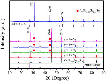 |
| | Fig. 1 XRD patterns of the Cu3Sb0.96Sn0.04Se4 matrix and Cu3Sb0.96Sn0.04Se4-yAgSb0.98Ge0.02Se2 (y = 1, 3, 5, 7 wt%) composite samples. The inset shows the XRD pattern of AgSb0.98Sn0.02Se2. | |
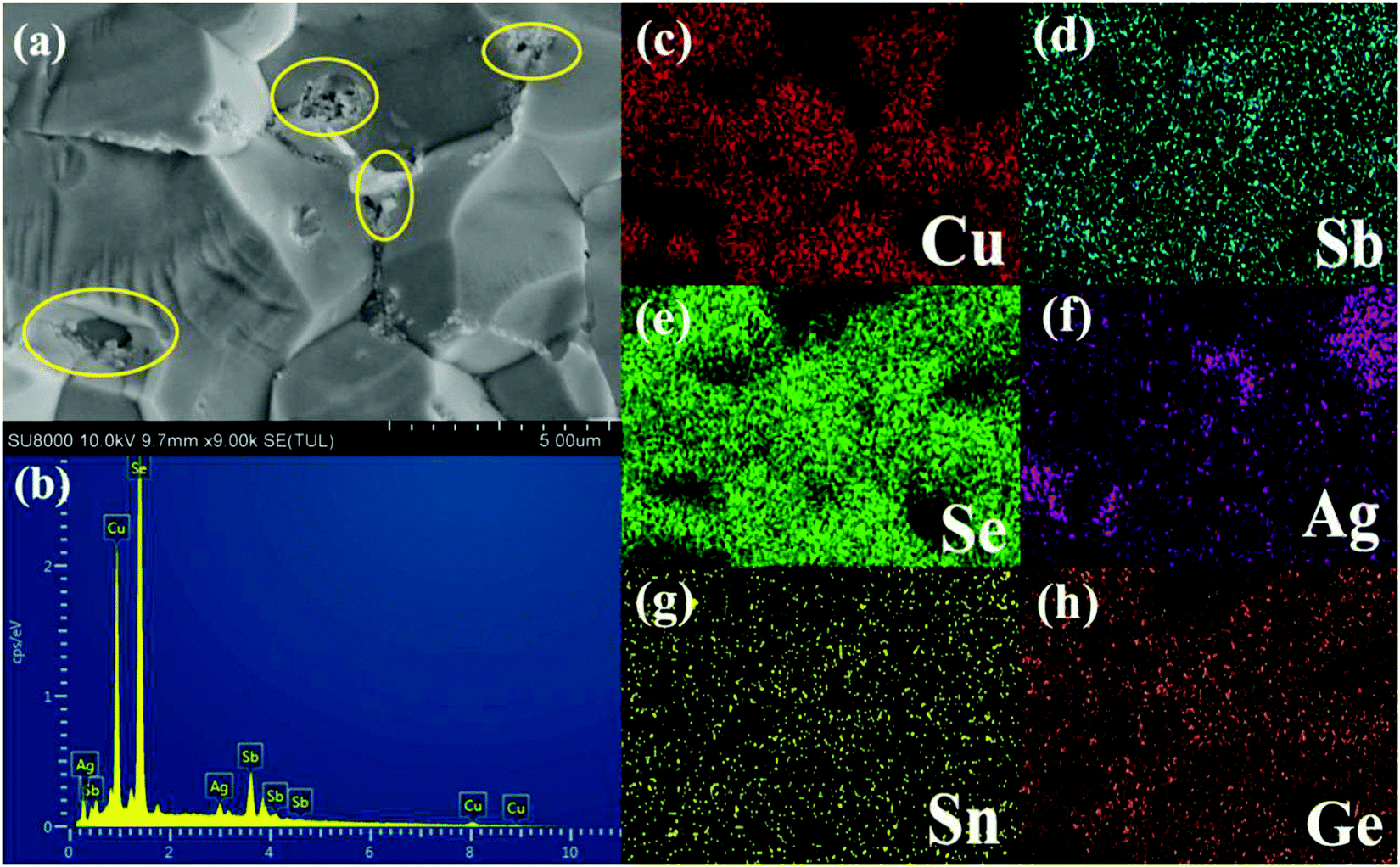
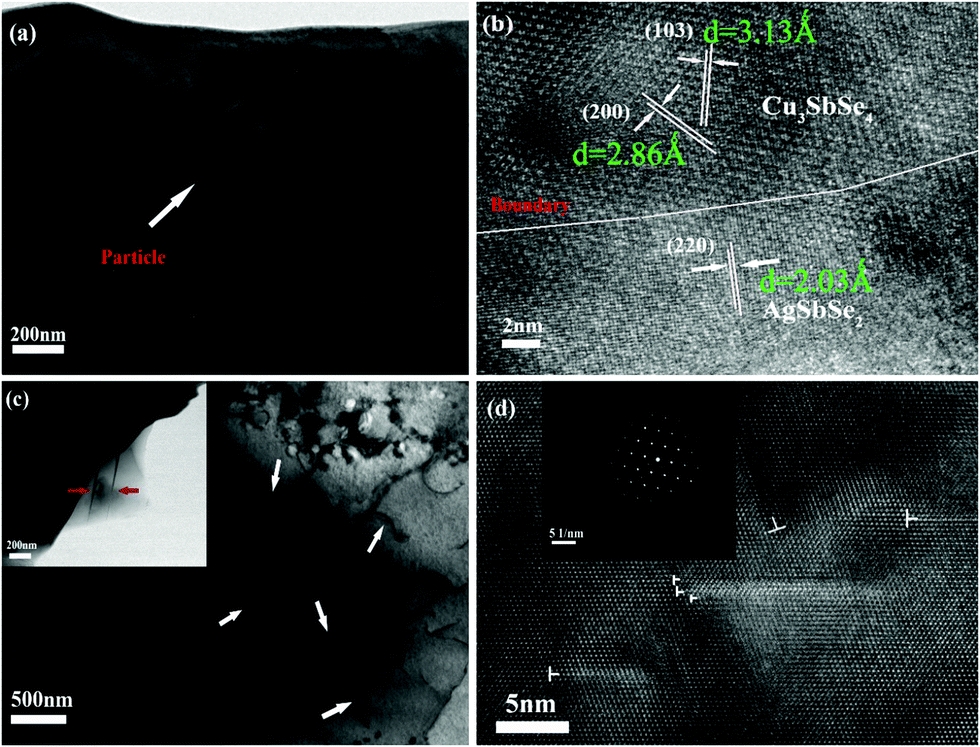
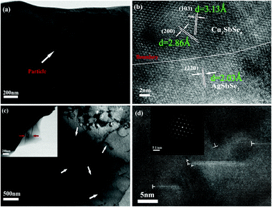
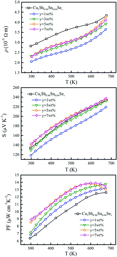
Fig. 2 shows the FESEM image of the fracture surface for the sample Cu3Sb0.96Sn0.04Se4-5 wt% AgSb0.98Ge0.02Se2. One can observe from Fig. 2(a) that many nanoparticles (marked by yellow ellipses) with a size of about 50–100 nm are embedded well in the Cu3Sb0.96Sn0.04Se4 matrix, which agrees well with the EDS analysis and elemental mapping, where the bright zones correspond to the AgSb0.98Ge0.02Se2-rich area. The SEM results confirmed that these particles are dispersed AgSb0.98Ge0.02Se2, indicating that Cu3Sb0.96Sn0.04Se4-yAgSb0.98Ge0.02Se2 (y = 1, 3, 5, 7 wt%) composites were prepared well. In order to further explore the microstructure of the composite samples, we conducted TEM analysis on Cu3Sb0.96Sn0.04Se4–5 wt% AgSb0.98Ge0.02Se2. As shown in Fig. 3(a), we observed that the particles with a size of around 200 nm are well embedded in the matrix with bright contrast. A high-resolution image is shown in Fig. 3(b).
 |
| | Fig. 2 (a) Morphology of the bulk fracture of the sample Cu3Sb0.96Sn0.04Se4-5 wt% AgSb0.98Ge0.02Se2; (b) EDS analysis of the areas marked in (a) by yellow ellipses; (c–h) EDX elemental mapping analysis of the sample Cu3Sb0.96Sn0.04Se4-5 wt% AgSb0.98Ge0.02Se2 corresponding to (a). | |
 |
| | Fig. 3 (a and b) Low magnification TEM image and HRTEM image for the bulk fracture of the sample Cu3Sb0.96Sn0.04Se4–5wt% AgSb0.98Ge0.02Se2; (c and d) low magnification TEM image and HRTEM image of the Cu3Sb0.96Sn0.04Se4 matrix and dislocation distribution; the inset shows the SAED image of the dislocation areas. | |
The matrices with interplanar distances of 3.13 Å and 2.86 Å correspond to the lattice planes of (1 0 3) and (2 0 0) of the doped tetragonal Cu3SbSe4 compound. The lattice spacing of about 2.03 Å corresponds to the (2 2 0) plane of cubic AgSbSe2. Obvious grain boundaries (GBs) are observed between the Cu3SbSe4 matrix and AgSbSe2 inclusions. We also find the existence of a large number of dislocations and faults in the matrix (marked with arrows). Fig. 3(c) and (d) present the low resolution and HRTEM images of a dislocation, where we can see clear dislocation lines and crystal defects such as twin crystals. From the SAED pattern of the dislocation line shown in the inset of Fig. 3(d), we can observe that many light diffraction circles are regularly arrayed between the diffraction spots of tetragonal Cu3SbSe4, which indicates the distinguished feature of dislocations in the crystal.
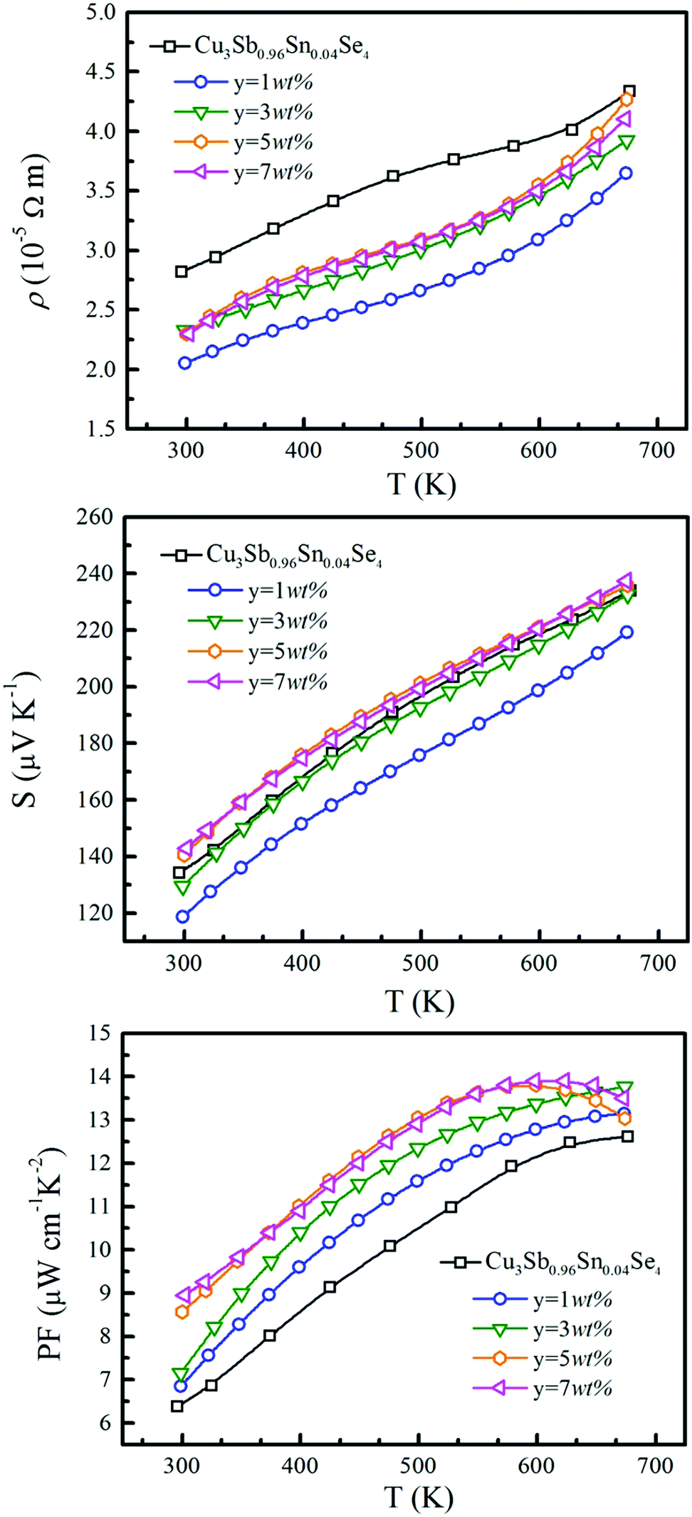
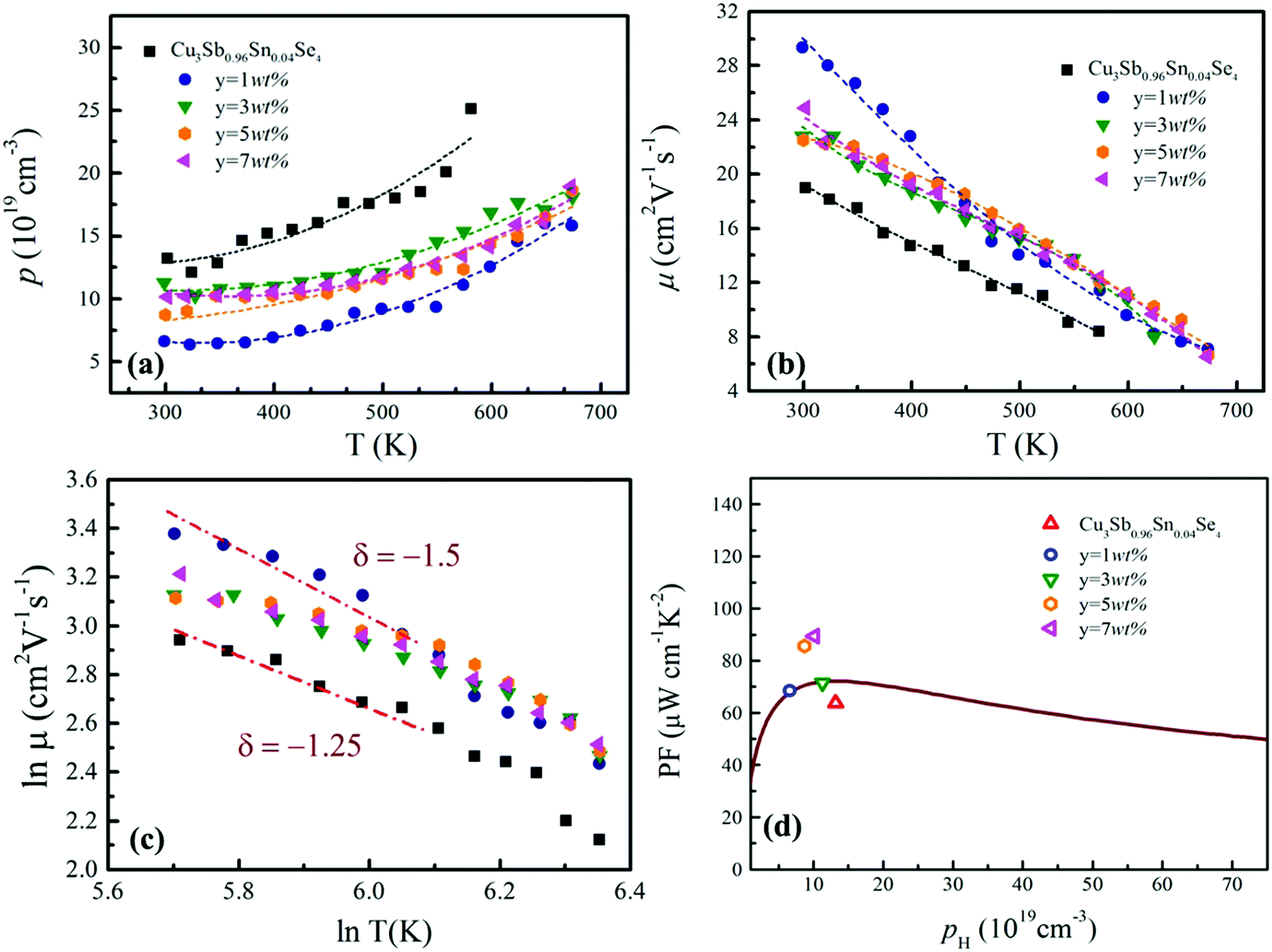
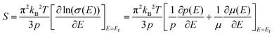
The temperature dependence of electrical resistivity (ρ) for samples of Cu3Sb0.96Sn0.04Se4–yAgSb0.98Ge0.02Se2 (y = 0, 1, 3, 5, and 7 wt%) is shown in Fig. 4(a). For all samples, ρ increases with increasing temperature, indicating representative degenerate semiconductor behavior. In addition, the existence of AgSb0.98Ge0.02Se2 inclusions causes a remarkable decrease of ρ for samples of Cu3Sb0.96Sn0.04Se4-yAgSb0.98Ge0.02Se2 (y = 1, 3, 5, and 7 wt%) in the whole temperature range investigated. For example, the ρ value decreases from 2.8 × 10⁻⁵ Ω m to 2.05 × 10⁻⁵ Ω m with y increasing from 0 to 1 wt% at 300 K, respectively. However, with the increase of the nanoparticle content, ρ of the composite samples increases slightly and there is no significant change with the variation of the second phase content. The variation in carrier concentration (p) for samples of Cu3Sb0.96Sn0.04Se4–yAgSb0.98Ge0.02Se2 (y = 0, 1, 3, 5, and 7 wt%) with temperature is shown in Fig. 5(a). It can be seen that the p value for all samples increases with increasing temperature, which is due to the thermal excitation of carriers. In addition, the p value decreases remarkably with a AgSb0.98Ge0.02Se2 content of 1 wt%, while it increases with further increasing the AgSb0.98Ge0.02Se2 content. For example, the p values at 300 K for samples with y = 0, 1, 3, 5, and 7 wt% are 1.32 × 1020 cm−3, 6.59 × 1019 cm−3, 1.13 × 1020 cm−3, 8.72 × 1019 cm−3, and 1.01 × 1020 cm−3, respectively. When the AgSb0.98Ge0.02Se2 nanoparticles are imbedded in the Cu3Sb0.96Sn0.04Se4 matrix, there are a lot of interfaces. A deep acceptor energy level will be formed, ascribed to interfacial defects, which can lead to a decrease in carrier concentration. However, due to the high carrier concentration of the AgSbSe2 system as compared to that of the Cu3SbSe4 system,19 the higher content of AgSb0.98Ge0.02Se2 embedded into the Cu3Sb0.96Sn0.04Se4 matrix will cause an increase of p as compared to the sample with y = 1 wt%.
 |
| | Fig. 4 Temperature dependence of electrical resistivity, Seebeck coefficient and power factor for composite samples Cu3Sb0.96Sn0.04Se4-yAgSb0.98Sn0.02Se2 (y = 1, 3, 5, and 7 wt%) in the temperature range from 300 K to 675 K. | |
 |
| | Fig. 5 (a) Temperature dependence of the carrier concentration; (b) plot of carrier mobility with temperature; (c and d) carrier concentration dependence of Seebeck coefficient (Pisarenko relation) and power factor at 300 K for all samples in this research. | |
The calculated values of carrier mobility (μ) are shown in Fig. 5(b). μ values for all composite samples are larger than that for the Cu3Sb0.96Sn0.04Se4 matrix. For instance, μ values at 300 K are 19 cm2 (V s)−1, 29.3 cm2 (V s)−1, 22.8 cm2 (V s)−1, 22.5 cm2 (V s)−1 and 24.8 cm2 (V s)−1 for samples with y = 0, 1, 3, 5 and 7 wt%, respectively. Meanwhile, we analyzed the relationship between ln![[thin space (1/6-em)]](https://www.rsc.org/images/entities/char_2009.gif) μ and lnT. As shown in Fig. 5(c), the calculated slope (δ) ranges from −1.25 to −1.5, indicating that the main mechanism of carrier scattering results from lattice vibration. The decrease of carrier concentration due to a deep acceptor energy level causes an increase in mobility. As the AgSb0.98Ge0.02Se2 content y is further increased, the decrease of mobility for the composite samples as compared to the sample with y = 1 wt% originates from the increasing grain boundaries. In this work, the trend of ρ with AgSb0.98Sn0.02Se2 content is determined by the mobility μ values for samples Cu3Sb0.96Sn0.04Se4-yAgSb0.98Ge0.02Se2 (y = 0, 1, 3, 5, and 7 wt%).
μ and lnT. As shown in Fig. 5(c), the calculated slope (δ) ranges from −1.25 to −1.5, indicating that the main mechanism of carrier scattering results from lattice vibration. The decrease of carrier concentration due to a deep acceptor energy level causes an increase in mobility. As the AgSb0.98Ge0.02Se2 content y is further increased, the decrease of mobility for the composite samples as compared to the sample with y = 1 wt% originates from the increasing grain boundaries. In this work, the trend of ρ with AgSb0.98Sn0.02Se2 content is determined by the mobility μ values for samples Cu3Sb0.96Sn0.04Se4-yAgSb0.98Ge0.02Se2 (y = 0, 1, 3, 5, and 7 wt%).
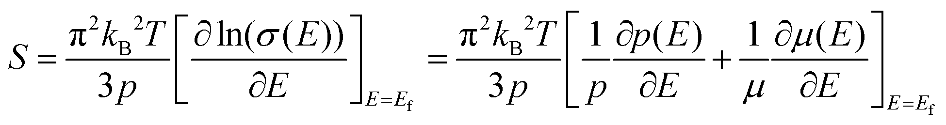
The temperature dependence of S is shown in Fig. 4(b), and the Seebeck coefficients for all the measured samples are positive in the whole temperature range of 300–675 K, indicating that they are p-type semiconductors. The S values of all samples increase monotonically and S decreases obviously with the increase of nanoinclusion content from y = 1 to 3, 5, and 7 wt%. In order to understand the electrical transport properties better, the Mott formula is given as follows:20
| |  | (1) |
where
kB,
Ef, and
p are the Boltzmann constant, Fermi energy, and carrier concentration, respectively. From
eqn (1), it can be seen that
S is inversely proportional to carrier concentration and mobility. For the specimen Cu
3Sb
0.96Sn
0.04Se
4–1 wt% AgSb
0.98Ge
0.02Se
2, the carrier concentration is decreased, while the mobility
μ increases largely, which causes a decrease of
S value compared with the matrix. With increasing AgSb
0.98Ge
0.02Se
2 content
y, the decrease of
p determines the
S value. The power factor calculated using the formula PF =
S2/
ρ is presented in
Fig. 4(c). We can observe that the power factors for composite samples have greatly increased compared with Cu
3Sb
0.96Sn
0.04Se
4. In particular, PF for the sample Cu
3Sb
0.96Sn
0.04Se
4–5 wt% AgSb
0.98Ge
0.02Se
2 increases from 8.56 × 10
−4 W m
−1 K
−2 to 1.3 × 10
−3 W m
−1 K
−2 with increasing temperature from 300 K to 675 K, which is a 15% improvement as compared to the Cu
3Sb
0.96Sn
0.04Se
4 matrix in the whole temperature range measured. The largest power factor obtained in this work is 1.38 × 10
−3 W m
−1 K
−2 for the sample Cu
3Sb
0.96Sn
0.04Se
4–5 wt% AgSb
0.98Ge
0.02Se
2, which is attributed to the increased mobility. The relationship between the carrier concentration and power factor is shown in
Fig. 5(d). The result indicates that although carrier concentration decreases as compared to the matrix, the increase of carrier mobility still plays a leading role in enhancing the power factor.
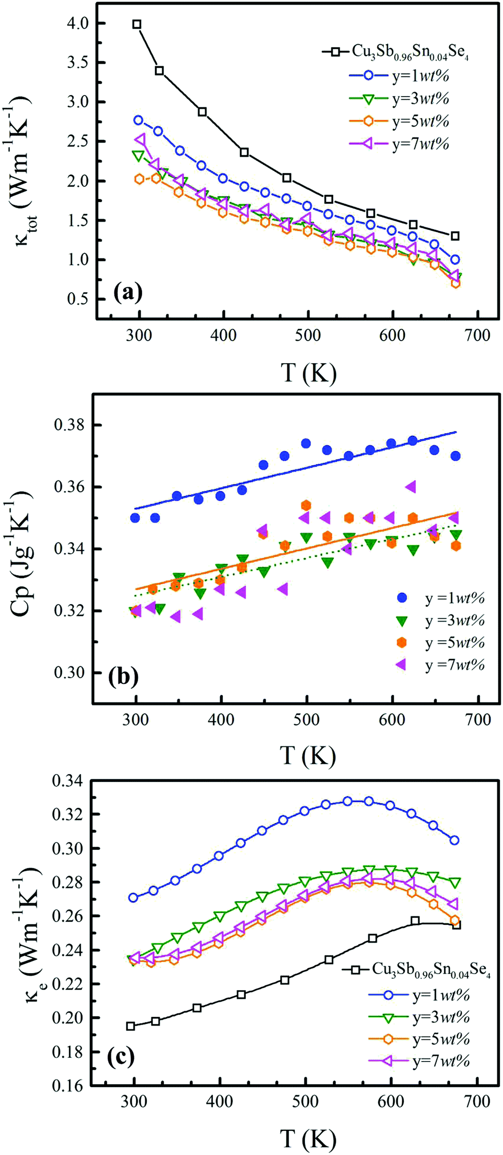
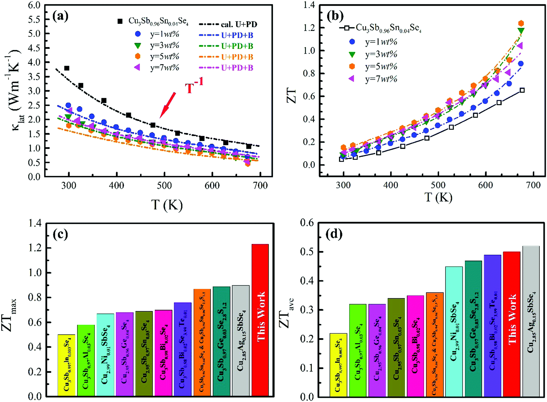
Fig. 6(a) shows the temperature dependence of total thermal conductivity (κtot) for samples Cu3Sb0.96Sn0.04Se4-yAgSb0.98Ge0.02Se2 (y = 0, 1, 3, 5, and 7 wt%). κtot decreases with increasing temperature. Moreover, κtot decreases monotonically with increasing AgSb0.98Ge0.02Se2 content (except for the sample with y = 7 wt%). For instance, κtot at 300 K drops from 3.98 W m−1 K−1 to 2.76, 2.33 and 2.02 W m−1 K−1 as y increases from 0 to 1, 3, and 5 wt%, respectively. In addition, as compared to the matrix, κtot of all composites decreases quickly at high temperatures (above 625 K). The results of the specific heat Cp measured via DSC for samples Cu3Sb0.96Sn0.04Se4-yAgSb0.98Ge0.02Se2 (y = 1, 3, 5, and 7 wt%) from 300 K to 675 K are shown in Fig. 6(b). One can see that the values of Cp for all samples are in the range from 0.32 to 0.37 J g−1 K−1, which is consistent with the theoretical value.21 To further analyze the thermal properties of the samples, the total thermal conductivity can be separated into two parts: carrier thermal conductivity and lattice thermal conductivity, as follows: κtot = κe + κL, where κe can be estimated using the Wiedemann–Franz relation, which is given by κe = LT/ρ, where the Lorenz number L is obtained using the Fermi integral function:21
| |  | (2) |
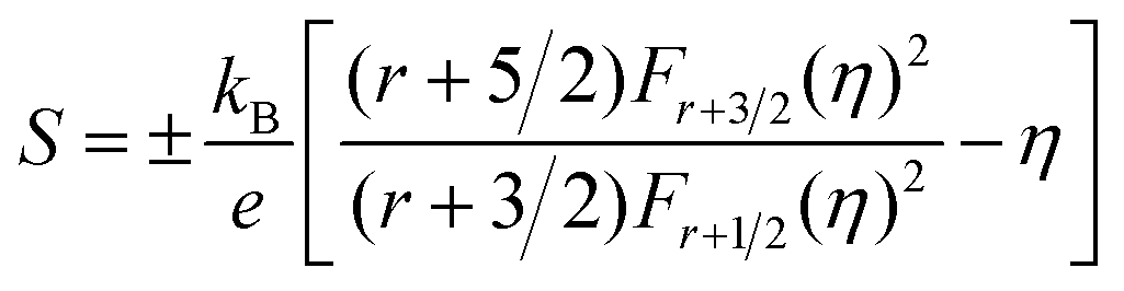
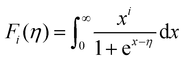
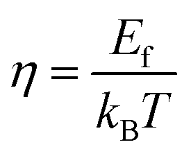
In the SPB model, the scattering factor can be assumed as
r = −1/2. So, the reduced Fermi energy (
η) used above can be calculated from the experimental
S values by using the following relationships:
| |  | (3) |
| |  | (4) |
| |  | (5) |
On the basis of the above calculation, the obtained
L value ranges from 1.79 × 10
−8 V
2 K
−2 to 1.86 × 10
−8 V
2 K
−2, as shown in Fig. S1 (ESI
†). As demonstrated in
Fig. 6(c),
κe initially increases with temperature and then slightly declines above 575 K for all samples.
κL for Cu
3Sb
0.96Sn
0.04Se
4 follows a law of
T−1 (shown in
Fig. 7(a)), indicating that phonon–phonon scattering (Umklapp scattering) dominates
22 and
κL for samples Cu
3Sb
0.96Sn
0.04Se
4-
yAgSb
0.98Ge
0.02Se
2 (
y = 1, 3, 5, and 7 wt%) decreases across the whole temperature range investigated with increasing AgSb
0.98Ge
0.02Se
2 content
y. Remarkably,
κL for the sample with
y = 5 wt% at 300 K is 1.79 W m
−1 K
−1, which is 53% smaller than that of the matrix sample. Nevertheless,
κL for the sample with
y = 7 wt% does not further decrease as
y increases, which can be ascribed to the agglomeration of nanoparticles. To understand the reduction of the lattice thermal conductivity, we introduce the Debye model and the lattice thermal conductivity
κL can be expressed using the Callaway equation as
| |  | (6) |
where
h,
θ,
v,
ζ, and
τ are the Planck constant, Debye temperature, phonon velocity, usual dimensionless variable and phonon relaxation time, respectively. The phonon relaxation time is mainly related to scattering from multiple scattering centers in composite samples according to Matthiessen's rule, where
τ can be written as
23| | | τ−1 = τPD−1 + τU−1 + τN−1 + τB−1 + τD−1 | (7) |
where
τPD−1,
τU−1,
τN−1,
τB−1 and
τD−1 are the relaxation times corresponding to scattering from point defects, phonon–phonon interactions, nanoparticles, boundaries and dislocations, respectively. For the Cu
3Sb
0.96Sn
0.04Se
4 matrix, the Umklapp process and point defects are the dominant mechanisms of phonon scattering. In the case of the nanocomposite samples, there are numerous nanoparticles playing a vital role in scattering low frequency phonons at low temperatures, which can explain the reason for the sharp decrease of
κL near room temperature. Therefore, the combined scattering rate
τ−1 for samples Cu
3Sb
0.96Sn
0.04Se
4-
y wt% AgSb
0.98Ge
0.02Se
2 (
y = 1, 3, 5, and 7 wt%) can be written as
| | | τ−1 = τPD−1 + τU−1 + τB−1 = Aω4 + Bω2Texp(−θ/3T) + ν/L | (8) |
where
A and
B are simplified parameters and
L is the distance between nanoparticles (detailed calculation parameters are listed in Table S1, ESI
†). As can be seen from the fitting results, with the increase of the content of the second phase, the phonon scattering from the point defects and nanoparticles increases first and then weakens, while the distance between nanoparticles initially decreases and then increases as the AgSb
0.98Ge
0.02Se
2 content
y is increased to 7 wt%, which should be ascribed to the agglomeration of the second phase. As shown in
Fig. 7(a), the calculated
κL values using the
U + PD +
B model match well with the experimental value of
κL for samples Cu
3Sb
0.96Sn
0.04Se
4-
yAgSb
0.98Ge
0.02Se
2 (
y = 1, 3, 5, and 7 wt%). The results confirm that the phonon scattering from the grain boundaries of AgSb
0.98Ge
0.02Se
2 nanoparticles is the main reason for the reduction of
κL compared with the matrix. The minimum lattice thermal conductivity observed in this work is consistent with the calculated limit of lattice thermal conductivity
κmin (around 0.4 W m
−1 K
−1),
24 which is 62% lower than that of the Cu
3Sb
0.96Sn
0.04Se
4 matrix.
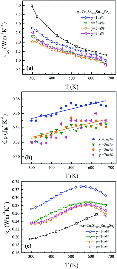 |
| | Fig. 6 Temperature dependence of (a) total thermal conductivity (κ); (b) special heat capacity (Cp); (c) thermal conductivity contributed from carriers (κe); (d) lattice thermal conductivity (κL) for Cu3Sb0.96Sn0.04Se4 and Cu3Sb0.96Sn0.04Se4–yAgSb0.98Ge0.02Se2 composite samples in the temperature range of 300–673 K. | |
 |
| | Fig. 7 (a) Comparison between the experimental data and calculated values of lattice thermal conductivity; (b) ZT values for all samples in the whole temperature range; comparison of the reported (c) ZTmax and (d) ZTave values of Cu3SbSe4 based materials that were synthesized using a melting method or solid state reaction. | |
The ZT values for samples Cu3Sb0.96Sn0.04Se4-yAgSb0.98Ge0.02Se2 (y = 0, 1, 3, 5, and 7 wt%) are shown in Fig. 7(b), from which one can see that the temperature behavior of ZT for all five samples is similar: it increases with temperature. The ZT values of the composite samples increase greatly compared with that of the matrix. In particular, a maximum ZT of 1.23 is achieved at 675 K for the composite sample with y = 5 wt%, which is almost twice that of Cu3Sb0.96Sn0.04Se4. Clearly, this significant improvement of ZT can be attributed to the simultaneous enhancement of power factor and remarkable reduction of thermal conductivity. Among all the reported Cu3SbSe4 materials, our sample Cu3Sb0.96Sn0.04Se4–5 wt% AgSb0.98Ge0.02Se2 exhibits the greatest thermoelectric performance (shown in Fig. 7(c)).8,16,24–34 Meanwhile, we calculated the average ZT (ZTave) value of our sample and other samples according to the relationship:
| | 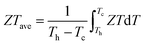 | (9) |
where
Th and
Tc are the temperatures of the hot-side and cold-side, respectively. As demonstrated in
Fig. 7(d), the largest
ZTave reaches 0.5 for the sample Cu
3Sb
0.96Sn
0.04Se
4-5 wt% AgSb
0.98Ge
0.02Se
2, which is 38% larger that of a previously reported composite sample.
16
Conclusion
In this work, high thermoelectric performance was obtained in composite samples Cu3Sb0.96Sn0.04Se4-yAgSb0.98Ge0.02Se2 (y = 1, 3, 5, and 7 wt%) obtained using melting and spark plasma sintering methods. The highest ZT of 1.23 was achieved for the sample Cu3Sb0.96Sn0.04Se4–3 wt% AgSb0.98Ge0.02Se2 at 675 K. This outstanding improvement is attributed to the enhancement of power factor and the reduced lattice thermal conductivity due to the incorporation of AgSb0.98Ge0.02Se2 inclusions. The obtained ZT = 1.23 is almost twice that of the Cu3Sb0.96Sn0.04Se4 matrix, which demonstrates that imbedding the second phase AgSb0.98Ge0.02Se2 is a promising strategy to enhance the thermoelectric properties of the Cu3SbSe4 system.
Conflicts of interest
There are no conflicts to declare.
Acknowledgements
This work was supported by funding from the Natural Science Foundation of China under grant No. 51672278 and 11674322. We acknowledge Dr Z.W. Chen and Prof. Y. Z. Pei of Tong Ji University for their help in the measurement of Hall coefficient.
References
- L. E. Bell, Cooling, heating, generating power, and recovering waste heat with thermoelectric systems, Science, 2008, 321(5895), 1457–1461 CrossRef CAS.
- A. J. Minnich, M. S. Dresselhaus, Z. F. Ren and G. Chen, Bulk nanostructured thermoelectric materials: current research and future prospects, Energy Environ. Sci., 2009, 2(5), 466–479 RSC.
- G. H. Kim, L. Shao, K. Zhang and K. P. Pipe, Engineered doping of organic semiconductors for enhanced thermoelectric efficiency, Nat. Mater., 2013, 12(8), 719–723 CrossRef CAS.
- R. Venkatasubramanian, E. Siivola, T. Colpitts and B. O'Quinn, Thin-film thermoelectric devices with high room-temperature figures of merit, Nature, 2001, 413(6856), 597–602 CrossRef CAS.
- D. Li, R. Li, X. Y. Qin, J. Zhang, C. J. Song, L. Wang and H. X. Xin, Co-precipitation synthesis of Sn and/or S doped nanostructured Cu3Sb1−xSnxSe4−ySy with a high thermoelectric performance, CrystEngComm, 2013, 15(36), 7166–7170 RSC.
- S. N. Aliev, G. G. Gadzhiev and Y. Magomedo, Electrical Conductivity, Thermoelectric Power, and Thermal Conductivity of Cu3AsSe4 and Cu3SbSe4, Semiconductors, 1970, 3(11), 1437 Search PubMed.
- C. Y. Yang, F. Q. Huang, L. M. Wu and K. Xu, New stannite-like p-type thermoelectric material Cu3SbSe4, J. Phys. D: Appl. Phys., 2011, 44(29), 5 CrossRef.
- C. H. Chang, C. L. Chen, W. T. Chiu and Y. Y. Che, Enhanced thermoelectric properties of Cu3SbSe4 by germanium doping, Mater. Lett., 2017, 186, 227–230 CrossRef CAS.
- D. G. Zhao, D. Wu and L. Bo, Enhanced Thermoelectric Properties of Cu3SbSe4 Compounds via Gallium Doping, Energies, 2017, 10, 1524 CrossRef.
- D. Do, V. Ozolins, S. D. Mahanti, M. S. Lee, Y. S. Zhang and C. Wolverton, Physics of bandgap formation in Cu–Sb–Se based novel thermoelectrics: the role of Sb valency and Cu d levels, J. Phys.: Condens. Matter, 2012, 24(41), 7 CrossRef.
- T. Zhou, L. J. Wang, S. Q. Zheng, M. Hong, T. Fang, P. P. Bai, S. Y. Chang, W. L. Cui, X. L. Shi, H. Z. Zhao and Z. G. Chen, Self-assembled 3D flower-like hierarchical Ti-doped Cu3SbSe4 microspheres with ultralow thermal conductivity and high zT, Nano Energy, 2018, 49, 221–229 CrossRef CAS.
- B. Y. Wang, S. Q. Zheng, Q. Wang, Z. L. Li, J. Li, Z. P. Zhang, Y. Wu, B. S. Zhu, S. Y. Wang, Y. X. Chen, L. Q. Chen and Z. G. Chen, Synergistic modulation of power factor and the thermal conductivity in Cu3SbSe4 towards high thermoelectric performance, Nano Energy, 2020, 71, 104658 CrossRef CAS.
- D. Li, R. Li, X. Y. Qin, C. J. Song, H. X. Xin, L. Wang, J. Zhang, G. L. Guo, T. H. Zou, Y. F. Liu and X. G. Zhu, Co-precipitation synthesis of nanostructured Cu3SbSe4 and its Sn-doped sample with high thermoelectric performance, Dalton Trans., 2014, 43(4), 1888–1896 RSC.
- Y. B. Luo, J. Y. Yang, Q. H. Jiang, W. X. Li, Y. Xiao, L. W. Fu, D. Zhang, Z. W. Zhou and Y. D. Cheng, Large enhancement of thermoelectric performance of CuInTe2via a synergistic strategy of point defects and microstructure engineering, Nano Energy, 2015, 18, 37–46 CrossRef CAS.
- C. Kim, J. Y. Baek, D. H. Lopez, D. H. Kim and H. Kim, Interfacial energy band and phonon scattering
effect in Bi2Te3-polypyrrole hybrid thermoelectric material, Appl. Phys. Lett., 2018, 113(15), 153901 CrossRef.
- J. M. Li, D. Li, C. J. Song, L. Wang, H. X. Xin, J. Zhang and X. Y. Qin, Realized high power factor and thermoelectric performance in Cu3SbSe4, Intermetallics, 2019, 109, 68–73 CrossRef CAS.
- W. H. Gao, Z. Y. Wang, J. Huang and Z. H. Liu, Extraordinary Thermoelectric Performance Realized in Hierarchically Structured AgSbSe2 with Ultralow Thermal Conductivity, ACS Appl. Mater. Interfaces, 2018, 10(22), 18685–18692 CrossRef CAS.
- D. Li, X. Y. Qin, T. H. Zou, J. Zhang, B. J. Ren, C. J. Song, Y. F. Liu, L. Wang, H. X. Xin and J. C. Li, High thermoelectric properties for Sn-doped AgSbSe2, J. Alloys Compd., 2015, 635, 87–91 CrossRef CAS.
- T. R. Wei, H. Wang, Z. M. Gibbs, C. F. Wu, G. J. Snyder and J. F. Li, Thermoelectric properties of Sn-doped p-type Cu3SbSe4: a compound with large effective mass and small band gap, J. Mater. Chem. A, 2014, 2(33), 13527–13533 RSC.
- S. N. Guin, A. Chatterjee, D. S. Negi, R. Datta and K. Biswas, High thermoelectric performance in tellurium free p-type AgSbSe2, Energy Environ. Sci., 2013, 6(9), 2603–2608 RSC.
- R. Fletcher, E. Zaremba, M. D'Iorio, C. T. Foxon and J. J. Harris, Persistent photoconductivity and two-band effects in GaAs/AlxGa1−xAs heterojunctions, Phys. Rev. B: Condens. Matter Mater. Phys., 1990, 41(15), 10649–10666 CrossRef CAS.
- T. H. Zou, X. Y. Qin, D. Li, L. L. Li, G. L. Sun, Q. Q. Wang, J. Zhang, H. X. Xin, Y. F. Liu and C. J. Song, Enhanced thermoelectric performance of beta-Zn4Sb3 based composites incorporated with large proportion of nanophase Cu3SbSe4, J. Alloys Compd., 2014, 588, 568–572 CrossRef CAS.
- Y. B. Luo, Q. H. Jiang, J. Y. Yang, W. X. Li, D. Zhang, Z. W. Zhou, Y. D. Cheng, Y. Y. Ren, X. He and X. Li, Simultaneous regulation of electrical and thermal transport properties in CuInTe2 by directly incorporating excess ZnX (X = S, Se), Nano Energy, 2017, 32, 80–87 CrossRef CAS.
- Q. H. Zhang, X. Ai, L. J. Wang, Y. X. Chang, W. Luo, W. Jiang and L. D. Chen, Improved Thermoelectric Performance of Silver Nanoparticles-Dispersed Bi2Te3 Composites Deriving from Hierarchical Two-Phased Heterostructure, Adv. Funct. Mater., 2015, 25(6), 966–976 CrossRef CAS.
- Y. B. Luo, J. Y. Yang, Q. H. Jiang, W. X. Li, D. Zhang, Z. W. Zhou, Y. D. Cheng, Y. Y. Ren and X. He, Progressive Regulation of Electrical and Thermal Transport Properties to High-Performance CuInTe2 Thermoelectric Materials, Adv. Energy Mater., 2016, 6(12), 10 Search PubMed.
- D. Li, J. M. Li, J. C. Li, Y. S. Wang, J. Zhang, X. Y. Qin, Y. Cao, Y. S. Li and G. D. Tang, High thermoelectric performance of n-type Bi(2)Te(2.7)Se(0.3)via nanostructure engineering, J. Mater. Chem. A, 2018, 6(20), 9642–9649 RSC.
- A. Kumar, P. Dhama and P. Banerji, Enhanced thermoelectric properties in Bi and Te doped p-type Cu3SbSe4 compound, AIP Conf. Proc., 2018, 1942, 140055 CrossRef.
- A. Kumar, P. Dhama, A. Das, K. J. Sarkar and P. Banerji, Enhanced electrical transport and thermoelectric properties in Ni doped Cu3SbSe4, AIP Conf. Proc., 2018, 1953, 050030 CrossRef.
- X. Y. Li, D. Li, H. X. Xin, J. Zhang, C. J. Song and X. Y. Qin, Effects of bismuth doping on the thermoelectric properties of Cu3SbSe4 at moderate temperatures, J. Alloys Compd., 2013, 561, 105–108 CrossRef CAS.
- Y. Y. Li, X. Y. Qin, D. Li, X. Y. Li, Y. F. Liu, J. Zhang, C. J. Song and H. X. Xin, Transport properties and enhanced thermoelectric performance of aluminum doped Cu3SbSe4, RSC Adv., 2015, 5(40), 31399–31403 RSC.
- E. J. Skoug, J. D. Cain and D. T. Morelli, High thermoelectric figure of merit in the Cu3SbSe4–Cu3SbS4 solid solution, Appl. Phys. Lett., 2011, 98(26), 3 CrossRef.
- D. Zhang, J. Y. Yang, H. C. Bai, Y. B. Luo, B. Wang, S. H. Hou, Z. L. Li and S. F. Wang, Significant average ZT enhancement in Cu3SbSe4-based thermoelectric material via softening p–d hybridization, J. Mater. Chem. A, 2019, 7(29), 17648–17654 RSC.
- D. Zhang, J. Y. Yang, Q. H. Jiang, L. W. Fu, Y. Xiao, Y. B. Luo and Z. W. Zhou, Improvement of thermoelectric properties of Cu3SbSe4 compound by In doping, Mater Des., 2016, 98, 150–154 CrossRef CAS.
- D. T. Morelli, J. P. Heremans and G. A. Slack, Estimation of the isotope effect on the lattice thermal conductivity of group IV and group III–V semiconductors, Phys. Rev. B: Condens. Matter Mater. Phys., 2002, 66(19), 195304 CrossRef.
Footnote |
| † Electronic supplementary information (ESI) available. See DOI: 10.1039/d0qm00553c |
|
| This journal is © the Partner Organisations 2021 |
Click here to see how this site uses Cookies. View our privacy policy here. 
 *a,
X. Y.
Qin
*a,
X. Y.
Qin