
 Open Access Article
 This Open Access Article is licensed under a Creative Commons Attribution-Non Commercial 3.0 Unported Licence
High resolution patterning of PbS quantum dots/graphene photodetectors with high responsivity via photolithography with a top graphene layer to protect surface ligands†
Seungbae
Ahn
 ,
Wenjun
Chen
and
Oscar
Vazquez-Mena
*
,
Wenjun
Chen
and
Oscar
Vazquez-Mena
*
Department of Nanoengineering, Center for Memory and Recording Research, Calibaja Center for Resilient Materials and Systems, University of California San Diego, 9500 Gilman Drive, La Jolla, CA 92093, USA. E-mail: oscarvm@eng.ucsd.edu
First published on 27th August 2021
Abstract
Photodetectors based on colloidal quantum dots (CQDs) and single layer graphene (SLG) have shown high responsivity due to the synergy of strong light absorption from CQDs and high mobility from SLG. However, it is still challenging to achieve high-density and small-footprint devices on a chip to meet the demand for their integration into electronic devices. Even though there are numerous approaches to pattern the chemically fragile CQD films, usually they require non-conventional approaches such as stamping and surface modification that may be non-compatible with semiconductor processing. In this study, we show that conventional lithography and dry etching can be used to pattern QD active films by employing a graphene monolayer passivation/protective layer that protects the surface ligands of CQDs. This protective layer avoids damage induced by lithography process solvents that deteriorate the carrier mobility of CQDs and therefore the photoresponse. Herein we report patterning of CQDs using conventional UV photolithography, achieving reproducible five-micron length PbS CQDs/SLG photodetectors with a responsivity of 108 A W−1. We have also fabricated thirty-six PbS CQDs/SLG photodetectors on a single chip to establish micron size photodetectors. This process offers an approach to pattern QDs with conventional UV lithography and dry etching semiconductor technology to facilitate their integration into current semiconductor commercial technology.
1. Introduction
Colloidal quantum dots (CQDs) are promising nanomaterials for light emission and detection applications because of their unique characteristics1 such as tunable band gaps that cover ultraviolet (UV), visible (Vis), and infrared (IR) bands (λ: 300 nm to 8 μm) depending on their composition (e.g. ZnO, CdS, PbS, GaAs, and HgTe) and size.2–4 Optical properties such as high absorption and emission are very attractive for various applications such as photovoltaics, photodetectors, and light-emitting diodes.5,6 Moreover inorganic semiconductors offer high-speed performance and the Gr/QD system offers ultrathin and flexible active films with high-responsivity that are important in biomedical applications. Even though there have been various studies to improve the efficiency and stability of CQDs,7,8 there are still limitations regarding the patterning techniques compatible with conventional semiconductor processing to facilitate their integration into electronic devices. The ligands required to stabilize films and facilitate charge transport are chemically fragile with respect to chemicals involved in conventional lithography processes such as photoresists, developers and resist removers. The proposed methods allowing CQD patterning include jet printing,9 dip-pen nanolithography,10 contact-printing,11 light-driven ligand cross-linking,12 assisted patterning,13 and direct extreme ultraviolet and electron-beam lithography.14 However, there is still a challenging trade-off between processing complexity, resolution and cost. For example, direct patterning methods such as jet printing, dip-pen nanolithography, and contact-printing have been extensively developed, but they still fall short of current industrial demands in terms of resolution, throughput rate, and uniformity. Light-driven ligand crosslinking patterning can achieve high resolution, but it requires specific light-sensitive ligands. Conventional UV photolithography has strong limitations since the photoresist and developer react with the short-chain ligands on CQDs, causing performance degradation.In this study, we developed an effective patterning technique that uses conventional UV photolithography and dry etching of CQDs by means of a poly(methyl methacrylate) (PMMA)/single layer graphene (SLG) passivation layer (PGPL) to prevent the damage of the CQD surface ligands by photolithography chemicals. This is extremely relevant since damage of the QD surface ligands can result in severe degradation of photocarrier transfer in the QD film and therefore in the photodetection performance. There have been numerous reports showing the use of SLG as an impermeable layer for various liquids and gases, allowing the protection of chemically fragile structures.12,13 Based on this report, we use SLG to protect the QD ligands during the pattering process to successfully pattern PbS QD films, achieving minimum features of 10 μm by 10 μm squares and line arrays with a 3 μm pitch. More importantly, we demonstrate the fabrication of PbS QDs/SLG photodetectors with different SLG channel lengths (5, 10, 20, 50, 100, 200, and 500 μm) showing higher responsivity and avoiding performance degradation as compared to devices fabricated without the protective layer. Since the photogain increases as the device length decreases, we achieve a high responsivity of 108 A W−1 with the smallest channel length of 5 μm. Also, thirty-six PbS QDs on SLG photodetectors have been fabricated to test the reliability after the patterning process.
2. Results and discussion
Fig. 1 shows the process flow for the patterning of CQDs on SLG with a PGPL via a conventional photolithography method to obtain CQD based photodetectors. The substrate has predefined Au electrodes prepared by lithography and lift-off with channel lengths of 5, 10, 20, 50, 100, 200, and 500 μm, and with a fixed width of 500 μm on top of SiO2, as shown in Fig. 1(a). Then the SLG layer as a conductive channel was transferred onto the substrate via PMMA supported wet transfer (Fig. 1(b)). The patterning of SLG using a AZ1518 photoresist and oxygen plasma etching is described in the Experimental section (Fig. 1(c)). SLG channels with a fixed width of 100 μm and varying channel lengths adapted to the 50–500 μm long predefined electrodes were patterned (Fig. SI.1(a)†). The patterned SLG substrate was coated with PbS CQDs via spin coating (Fig. 1(d)). The deposition of PbS CQDs and ligand exchange are described in the Experimental section. After that, the PGPL was transferred on top of the CQD film following conventional PMMA/Gr transfer in aqueous solution (Fig. 1(e)). During PGPL transfer, the device is immersed in DI water; however, previous reports show that this process does not induce significant degradation of the light absorption of the PbS CQD film.15–17 The AZ1518 UV photoresist was spin coated on top of the PGPL, as shown in Fig. 1(f). The PGPL prevents the photoresist from permeating into PbS CQDs due to low permeability of PMMA and SLG. The photoresist was patterned and developed using conventional UV photolithography (Fig. 1(g)). The etching process was done in two steps. First, the top PGPL was etched using oxygen plasma. After that, the PbS CQDs were etched using a mixture of H2/CH4/Ar.18,19 After the etching process, the PGPL was removed by immersing in acetone and cleaned using IPA and DI water. The conditions for etching SLG and PbS QDs and the cleaning process are described in the Experimental section. A gas mixture of CH4/H2 plasma was commonly used for dry etching III–V and II–VI semiconducting materials. In the process, CH4 gas forms volatile metal organic species with lead, which is easily removed from the surface by Ar ions, and H2 forms volatile hydride species with sulfur. Optical pictures of the final patterned PbS CQDs/SLG photodetectors are shown in Fig. SI.1(b).† Our final devices have a bottom SLG that serves as a charge collector, the PbS CQD film that serves as a light absorber, and the top PGPL that protects the QDs during photolithography but also contributes to charge collection in this case. Fig. 1(i)–(k) show the scanning electron microscope (SEM) images of examples of different patterns of CQD films that illustrate the capabilities of our method to pattern CQD films. Fig. 1(i) shows a 2D array of 10 μm × 10 μm squares, Fig. 1(j) shows a line grid of 3 μm wide CQD films separated by 3 μm, and Fig. 1(k) shows the “UCSD Nanoengineering” legend. This patterned array of PbS CQDs shows no significant residue in regions where the etching process occurred. The inset in Fig. 1(k) shows images of the Pb signal from EDX. | ||
| Fig. 1 Schematic diagram of the patterning process of PbS CQDs using a PGPL. (a) Au (100 nm)/Cr (10 nm) electrodes were deposited using a e-beam evaporator with different channel lengths (5, 10, 20, 50, 100, 200, and 500 μm). (b) PMMA/SLG layer was transferred onto the prepatterned-electrode substrate via the PMMA supported wet transfer method. (c) SLG was patterned by the photolithography method with the same channel width (100 μm). (d) PbS CQDs were deposited by the spin-coating method with TBAI ligand exchange. (e) PGPL was transferred onto PbS CQDs on the patterned SLG substrate. (f) Photoresist was coated on the substrate. (g) The patterning was executed by the conventional UV photolithography process. (h) Exposed PGPL and PbS CQDs were removed by oxygen plasma and CH4/H2/Ar plasma, respectively. After that, the PGPL was removed using acetone, and cleaned using IPA, and DI (i) SEM image of the 10 μm × 10 μm square array. (j) SEM image of the 3 μm line array. (k) SEM image of “UCSD Nanoengineering” legend words. Inset: Pb EDX signal from SEM. | ||
In order to understand the possible effects of the photolithography process on the performance and chemistry of the CQDs, we investigated the lithography patterning with and without the protective layer by UV-Vis spectroscopy and Fourier transform infra-red spectroscopy (FTIR) of the CQDs. It is observed that the first absorption peak of pristine PbS CQDs is at 930 nm. However, after patterning without the PGPL, there is a blue shift of ∼35 nm and a reduction in the first absorption peak, as shown in Fig. 2(a). In contrast, when using the PGPL, the blue shift is limited to ∼6 nm (Fig. 2(b)) and the first exciton absorption peak is not reduced. We suggest that for the samples without the PGPL, the spectral modification is due to the formation of minibands in PbS QDs induced by electron coupling between adjacent QDs when the ligands are modified by the organic developer or photoresist.20 FTIR spectra are shown in Fig. 2(c), providing further insight into the surface chemistry of the CQDs during the lithography process and the impact of the PGPL. The FTIR spectra of the pristine (black trace) and patterned PbS CQDs with the PGPL (red trace) indicate the asymmetric C–H (2925 and 2956 cm−1) and symmetric C–H (2853 cm−1) vibrations, but no vibrational modes between 1400 and 1600 cm−1.21 On the other hand, the FTIR spectrum of the patterned PbS CQDs without the PGPL shows weaker stretching modes around 2900 cm−1, with additional CH bending modes (1461 cm−1) not present in the pristine and PGPL samples. The FTIR and UV-Vis spectra of the samples without the PGPL indicate a modification of the ligands probably due to resist and developer processing. Therefore, we infer that the PGPL plays an important role in protecting the chemistry of the CQDs during the lithography process.
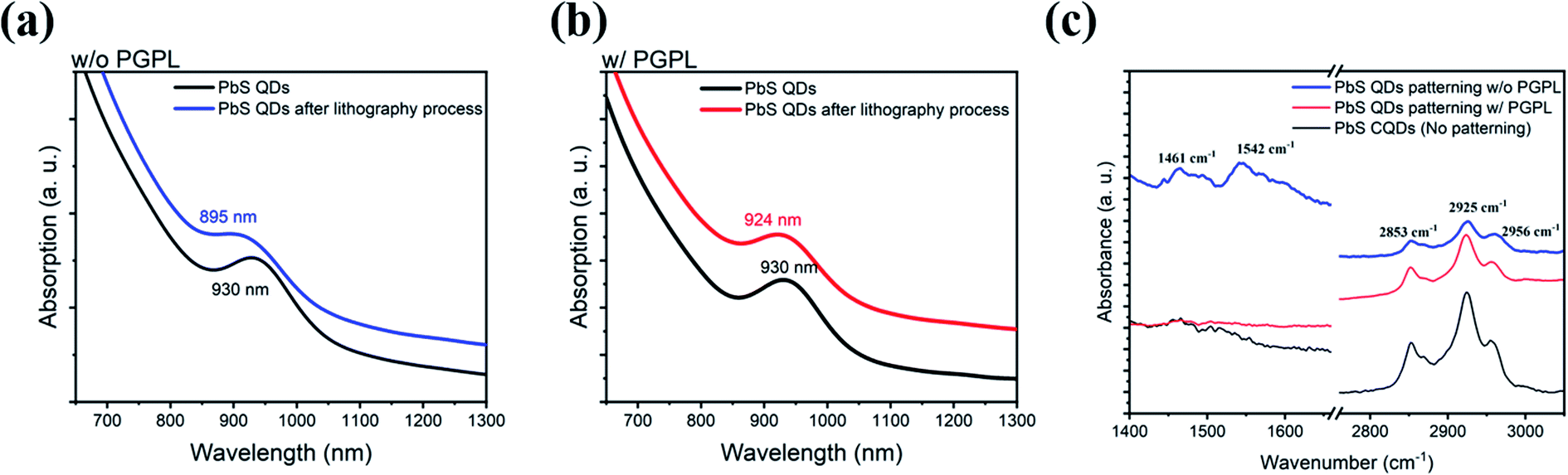 | ||
| Fig. 2 (a) UV-Vis absorption spectra of PbS CQDs without the PGPL, showing a shift of the resonance peak from 930 nm to 895 nm. (b) UV-Vis absorption spectra of PbS CQDs with the PGPL, representing a shift of the resonance peak from 930 nm to 924 nm. (c) FTIR spectra of the photoresist, pristine PbS CQDs, and the patterned PbS CQDs with and without the PGPL. | ||
The impact of the PGPL on the photoresponse of hybrid SLG/CQD photoconductive detectors was tested on devices with graphene channels of a length of 100 μm and width of 100 μm (underneath SLG, Fig. 1(c)) under λ = 635 nm illumination. The principle of the operation of the devices is shown in Fig. SI.2.† Light is absorbed by QDs generating photocarriers, followed by charge separation. In the specific case of Gr and PbS-QDs, due to band alignment and interface built-in potential, electrons remain in the QDs while holes are transferred to graphene. The transferred holes change the graphene (p-type) conductivity while the electrons generate a photogating effect. Non-patterned PbS CQDs on SLG (reference devices) and patterned PbS CQDs on SLG with and without the PGPL were tested. The thickness of the CQD film was ∼150 nm obtained by spin coating 5 CQD layers. More details about the sample preparation are given in the Experimental section. Fig. 3(a) shows the time-modulated response for the three devices. All cases show a similar time-modulated response with good time stability. Variations at the dark current base level can be due to variations in the resistance of SLG (Fig. SI.3†) probably associated with residues after PMMA/wet and SLG patterning. The reference performance is that of the device without CQD patterning, producing a photocurrent of 50 μA. If the QDs are patterned without the PGPL, the photocurrent drops significantly to ∼18 μA (blue trace). This is expected from the disorder and contamination induced by the photoresist during the patterning process. On the other hand, the patterned device with the PGPL results in a higher photocurrent of ∼63 μA. The dark current increases due to the top graphene of the PGPL which contributes to the conductivity of the device. Furthermore, the top SLG of the PGPL increases the responsivity as it helps to collect photocarriers and increases the photocurrent, as shown previously.17 Photo-excited carriers on the surface of PbS CQDs can be efficiently collected by the top graphene channel of the PGPL, instead of recombining while crossing the entire film thickness to reach the bottom SLG. However, it is important to remember that the critical role of the PGPL is to protect the ligands. Without the PGPL, lithography chemicals harm the ligands permanently, and even adding a PGPL after lithography does not recover the photoresponse. This is shown in Fig. SI.4,† which shows that without the PGPL, lithography induces damage and poor performance that cannot be recovered with the addition of the PGPL after lithography. Therefore the critical role of the PGPL is to protect the ligands during lithography. The enhanced collection by the top graphene of the PGPL is an added, but not essential, benefit. Regarding the time response, the devices show a long-time delay (>1 s) response which is due to trap states in the QDs22 and at the QD/Gr interface, as has been reported previously for hybrid Gr/QD systems.23,24 Passivation layers can be used to reduce the response delay.25,26 Fig. SI.5† shows 60 second time traces showing the stability of the photoresponse. Fig. 3(b) shows the spectral response, using a Hg–Xe lamp light source and a monochromator, showing a similar trend of superior performance for devices with the PGPL in the entire λ = 400–1000 nm range. The photoresponsivity as a function of power is shown in Fig. 3(c), showing the expected trend of higher responsivity for lower power in hybrid SLG/CQDs photodetectors, which is due to higher recombination at higher light intensity. Through a wide range of intensities, the patterned devices with the PGPL show superior performance. Fig. 3(d) shows the photoresponsivity for the shortest channel length of 5 μm with a 100 μm width. The 5 μm length PbS QDs on SLG photodetectors show a record high responsivity of 108 A W−1. This is expected as the photogain of the devices is proportional to the ratio of the lifetime τl of the photo-induced carrier over carrier transit time  , where L is the channel length, μ is the carrier mobility, and VDS is the drain–source voltage. As expected, the shorter 5 μm long channel results in a higher photogain and therefore higher photoresponsivity.
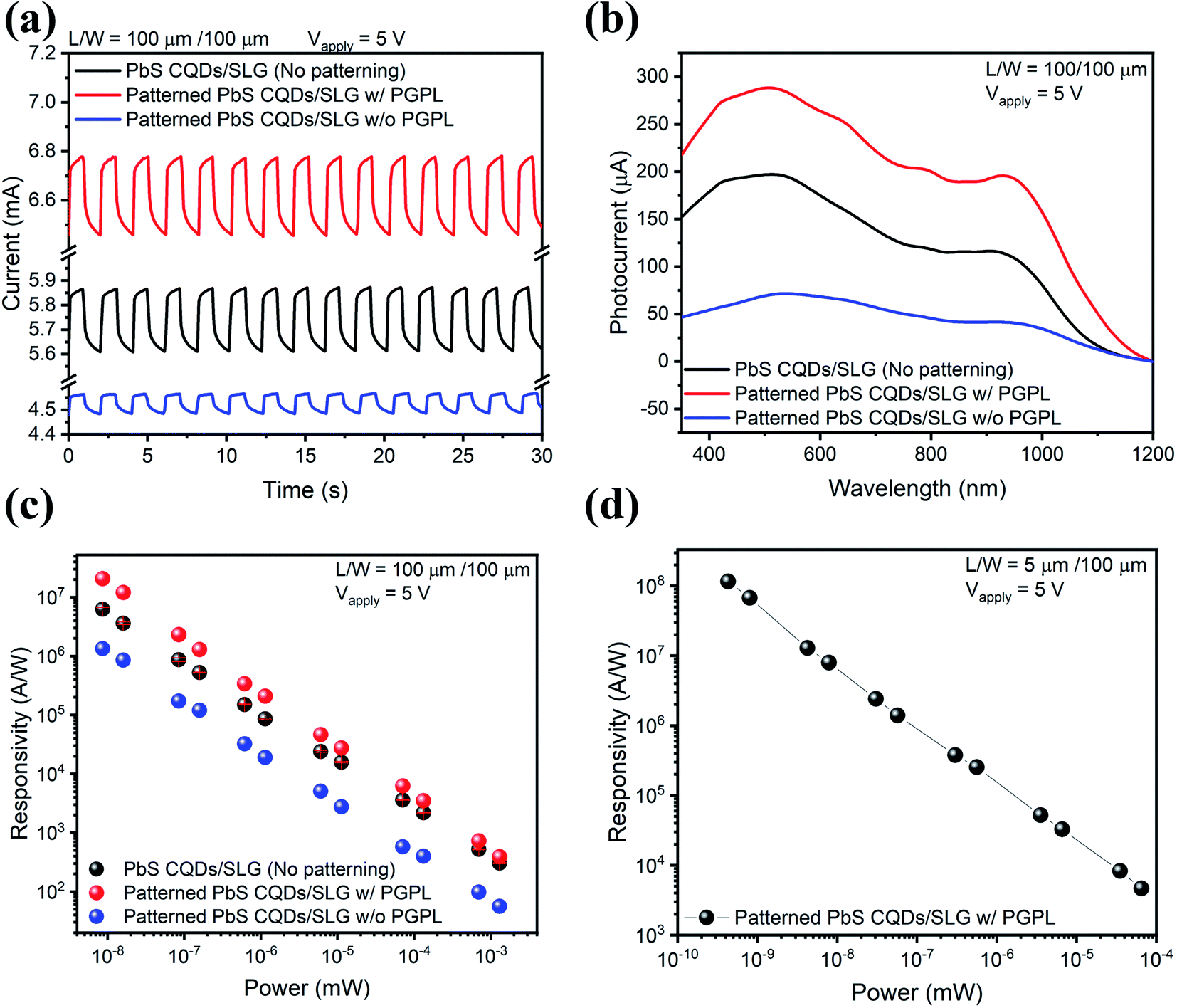 | ||
| Fig. 3 (a) Time response for on/off light switching of pristine PbS CQDs/patterned SLG, patterned PbS CQDs/SLG with the PGPL, and without the PGPL (Vbias = 5 V, λ = 635 nm, 17 mW cm−2). (b) Responsivity as a function of wavelength, showing the highest response for patterned PbS CQDs/SLG with the PGPL (Hg–Xe lamp with a monochromator). (c) Responsivity versus power, showing an increase in responsivity as the power decreases (λ = 635 nm). (d) Responsivity as a function of power (λ = 635 nm), showing that the shortest channel length of 5 μm achieves a responsivity of 108 A W−1. | ||
Our patterning technique allows us to fabricate an array of thirty-six PbS CQDs/SLG photodetectors with dimensions of 100 μm by 100 μm. Fig. 4(a) shows the optical images of the electrodes with patterned SLG and Fig. 4(b) shows the same chip after deposition and patterning of PbS CQDs with the PGPL protective layer. Patterning capabilities can be extremely important for hybrid QD/Gr image sensor arrays on CMOS platforms, as has been reported elsewhere with a pixel size of 3 μm based only on Gr patterning achieving detectivities of 1010–108 Jones.27 Patterning of QDs can improve the pixel resolution and reduce the noise, potentially achieving a detectivity of 1012 Jones for individual detectors. We measured the photoresponse of randomly selected six photodetectors on the chip. Fig. 4(c) shows responsivity versus incident power and Fig. 4(d) shows the spectral response, illustrating good uniformity in device characteristics. The detectivity (D*) is also investigated, as shown in Fig. 4(e), showing that the devices can reach D* ∼ 1012 Jones at low power (10−8 mW) at 40 Hz. The details of the noise measurements and detectivity calculations are shown in the Fig. SI.6.† The responsivity and detectivity of the devices improve significantly as the light intensity decreases. For large intensities, there is a significant increase in charge recombination, reducing the number of photocarriers transferred from the QDs to Gr. This behavior has been observed in previous reports on QD/Gr photodetectors6,23,24,26 as well for QD based photodetectors.28 As described elsewhere,6,23 the amount of charges transferred from QDs to Gr has a sub-linear dependence on the light intensity, resulting in an overall decrease in responsivity as light intensity increases.
 | ||
| Fig. 4 (a) Optical images of 100 μm by 100 μm patterned SLG. (b) Same devices after coating PbS CQDs/SLG, forming a photodetector array. (c) Responsivity as a function of power for the PbS CQDs/SLG photodetector array, showing small variations in the performance of the photodetectors in the array. (d) Photocurrent versus wavelength for the array, showing a reliable photocurrent response depending on the wavelength. (e) Detectivities versus incident power for the PbS CQDs/SLG photodetector array at 40 Hz. | ||
3. Conclusion
In conclusion, we report the high-resolution patterning of high-responsivity photodetectors based on PbS CQDs/SLG via conventional UV photolithography with a PGPL as an impermeable layer that prevents the damage of the surface ligands of the PbS CQDs during the UV photolithography and dry etching processes. The resolution of PbS CQD patterning can reach a few microns. The photoresponse for 5 μm length and 100 μm width PbS CQDs/SLG photodetectors has a high responsivity (>108 A W−1) and detectivity (∼1012 Jones). Moreover, the array of PbS CQDs/SLG photodetectors shows a reliable photoresponse for high responsivity and spectral response. The results provide an easy and promising patterning process for CQD based devices such as photodetectors.4. Experimental section
PbS QD synthesis
Lead oxide (0.94 g) was dissolved and degassed in 1-octadecene (25 ml) with oleic acid (4 ml) in a three-neck flask under vacuum at 90 °C for two hours. When the solution became clear, bis(trimethylsilyl) sulfide (420 μl) dissolved in 1-octadecene (12.8 ml) was injected into the solution. After that, the reaction was carried out for 30 seconds and cooled down by placing the flask in ice water. The solution was centrifuged, followed by cleaning with toluene and acetone three times, and then dissolved in toluene (30 mg ml−1) after filtration with a 250 nm pore size filter.29Graphene transfer
We purchased CVD-SLG on Cu coated with PMMA from Graphenea (Spain). The backside of Cu was etched using oxygen plasma. It was transferred to the substrate by the wet method. Cu was removed using ammonium persulfate solution. After Cu was completely etched, the PMMA/SLG layer was transferred to DI water to remove etching residues. Then, the PMMA/SLG layer was transferred onto a SiO2/Si substrate with Au electrodes, followed by drying for two hours at room temperature. Finally, the PMMA layer was removed using acetone and cleaned with isopropyl alcohol and DI water.Device fabrication
Optoelectronic characterization
The power of λ = 635 nm and 1.2 mW laser diode (CPS635R, Thorlabs) was measured by a standard silicon photodetector (S120VC, Thorlabs). The power intensity of the laser was achieved by using absorptive neutral density filters (NE503A, NE510A, NE520A, and NE530A, Thorlabs). Current–voltage and current–time data were measured through a Keithley 2400 source meter. Noise measurements for detectivity were extracted from the RMS noise of dark current traces. The spectral response was measured using a Keithley 2400 source meter using a 500 Watts mercury–xenon lamp and filters (66485-500HX-R1, USFW-100, Newport) with a monochromator (CS260-RG-3-FH-D, Newport).Materials characterization
The vibrational modes of PbS QDs were analyzed by FTIR spectroscopy (Nicolet 6700). The structural information of Gr was carefully investigated by Raman spectroscopy (Renishaw). The absorption spectra of PbS QDs were recorded by using a UV-Vis spectrophotometer (UH4150, Hitachi).Conflicts of interest
There are no conflicts to declare.Acknowledgements
This work was supported by the National Science Foundation under Award No. 1710472 and No. 2046176 (NSF CAREER). This work was performed in part at the San Diego Nanotechnology Infrastructure (SDNI) of UCSD, NANO3, a member of the National Nanotechnology Coordinated Infrastructure, which was supported by the National Science Foundation (Grant No. ECCS-1542148). S. A. was supported by the Kwanjeong Fellowship from the Kwanjeong Educational Foundation.References
- A. P. Litvin, I. V. Martynenko, F. Purcell-Milton, A. V. Baranov, A. V. Fedorov and Y. K. Gun’ko, Colloidal Quantum Dots for Optoelectronics, J. Mater. Chem. A, 2017, 5(26), 13252–13275, 10.1039/c7ta02076g.
- J. M. Pietryga, Y.-S. Park, J. Lim, A. F. Fidler, W. K. Bae, S. Brovelli and V. I. Klimov, Spectroscopic and Device Aspects of Nanocrystal Quantum Dots, Chem. Rev., 2016, 116(18), 10513–10622, DOI:10.1021/acs.chemrev.6b00169.
- S. B. Hafiz, M. Scimeca, A. Sahu and D.-K. Ko, Colloidal Quantum Dots for Thermal Infrared Sensing and Imaging, Nano Convergence, 2019, 6(1), 7, DOI:10.1186/s40580-019-0178-1.
- S. D. Gunapala, S. V. Bandara, C. J. Hill, D. Z. Ting, J. K. Liu, S. B. Rafol, E. R. Blazejewski, J. M. Mumolo, S. A. Keo, S. Krishna, et al., Long-Wavelength Infrared (LWIR) Quantum-Dot Infrared Photodetector (QDIP) Focal Plane Array, in Infrared Technology and Applications XXXII, ed. B. F. Andresen, G. F. Fulop and P. R. Norton, 2006, vol. 6206, p. 62060J, DOI:10.1117/12.662462.
- C. R. Kagan, E. Lifshitz, E. H. Sargent and D. V. Talapin, Building Devices from Colloidal Quantum Dots, Science, 2016, 353(6302), aac5523, DOI:10.1126/science.aac5523.
- S. Ahn, W. Chen, M. A. Moreno-Gonzalez, M. Lockett, J. Wang and O. Vazquez-Mena, Enhanced Charge Transfer and Responsivity in Hybrid Quantum Dot/Graphene Photodetectors Using ZnO as Intermediate Electron-Collecting Layer, Adv. Electron. Mater., 2020, 6(6), 2000014, DOI:10.1002/aelm.202000014.
- R. Wang, Y. Shang, P. Kanjanaboos, W. Zhou, Z. Ning and E. H. Sargent, Colloidal Quantum Dot Ligand Engineering for High Performance Solar Cells, Energy Environ. Sci., 2016, 9(4), 1130–1143, 10.1039/C5EE03887A.
- H. Moon, C. Lee, W. Lee, J. Kim and H. Chae, Stability of Quantum Dots, Quantum Dot Films, and Quantum Dot Light-Emitting Diodes for Display Applications, Adv. Mater., 2019, 31(34), 1804294, DOI:10.1002/adma.201804294.
- G. Azzellino, F. S. Freyria, M. Nasilowski, M. G. Bawendi and V. Bulović, Micron-Scale Patterning of High Quantum Yield Quantum Dot LEDs, Adv. Mater. Technol., 2019, 4(7), 1800727, DOI:10.1002/admt.201800727.
- S. Biswas, F. Brinkmann, M. Hirtz and H. Fuchs, Patterning of Quantum Dots by Dip-Pen and Polymer Pen Nanolithography, Nanofabrication, 2015, 2(1), 19–26, DOI:10.1515/nanofab-2015-0002.
- H. Keum, Y. Jiang, J. K. Park, J. C. Flanagan, M. Shim and S. Kim, Photoresist Contact Patterning of Quantum Dot Films, ACS Nano, 2018, 12(10), 10024–10031, DOI:10.1021/acsnano.8b04462.
- J. Yang, D. Hahm, K. Kim, S. Rhee, M. Lee, S. Kim, J. H. Chang, H. W. Park, J. Lim and M. Lee, et al., High-Resolution Patterning of Colloidal Quantum Dots via Non-Destructive, Light-Driven Ligand Crosslinking, Nat. Commun., 2020, 11(1), 2874, DOI:10.1038/s41467-020-16652-4.
- W. Zhou, L. Zheng, X. Cheng, W. Zhou, X. Xiao, K. Xu, W. Xin, P. Ye and Y. Yu, PbS Colloidal Quantum Dots Patterning Technique with Low Vertical Leakage Current for the Photodetection Applications, J. Mater. Sci.: Mater. Electron., 2020, 31(8), 5900–5906, DOI:10.1007/s10854-019-02819-3.
- C. D. Dieleman, W. Ding, L. Wu, N. Thakur, I. Bespalov, B. Daiber, Y. Ekinci, S. Castellanos and B. Ehrler, Universal Direct Patterning of Colloidal Quantum Dots by (Extreme) Ultraviolet and Electron Beam Lithography, Nanoscale, 2020, 12(20), 11306–11316, 10.1039/d0nr01077d.
- W. Chen, S. Ahn, M. Balingit, J. Wang, M. Lockett and O. Vazquez-Mena, Near Full Light Absorption and Full Charge Collection in 1-Micron Thick Quantum Dot Photodetector Using Intercalated Graphene Monolayer Electrodes, Nanoscale, 2020, 12(8), 4909–4915, 10.1039/c9nr09901h.
- W. Chen, S. Ahn, C. Rangel and O. Vazquez-Mena, Implementation of Metallic Vertical Interconnect Access in Hybrid Intercalated Graphene/Quantum Dot Photodetector for Improved Charge Collection, Front. Mater., 2019, 6, 159, DOI:10.3389/fmats.2019.00159.
- W. Chen, J. Castro, S. Ahn, X. Li and O. Vazquez-Mena, Improved Charge Extraction Beyond Diffusion Length by Layer-by-Layer Multistacking Intercalation of Graphene Layers inside Quantum Dots Films, Adv. Mater., 2019, 31(14), 1807894, DOI:10.1002/adma.201807894.
- M. A. Foad, C. D. W. Wilkinson, C. Dunscomb and R. H. Williams, CH4/H2: A Universal Reactive Ion Etch for II–VI Semiconductors?, Appl. Phys. Lett., 1992, 60(20), 2531–2533, DOI:10.1063/1.106929.
- G. Yang and B. Weng, Reactive Ion Etching of PbSe Thin Films in CH4/H2/Ar Plasma Atmosphere, Mater. Sci. Semicond. Process., 2021, 124, 105596, DOI:10.1016/j.mssp.2020.105596.
- S. Aynehband, M. Mohammadi, K. Thorwarth, R. Hany, F. A. Nüesch, M. D. Rossell, R. Pauer, J.-M. Nunzi and A. Simchi, Solution Processing and Self-Organization of PbS Quantum Dots Passivated with Formamidinium Lead Iodide (FAPbI3), ACS Omega, 2020, 5(25), 15746–15754, DOI:10.1021/acsomega.0c02319.
- B.-S. Kim, J. Hong, B. Hou, Y. Cho, J. I. Sohn, S. Cha and J. M. Kim, Inorganic-Ligand Exchanging Time Effect in PbS Quantum Dot Solar Cell, Appl. Phys. Lett., 2016, 109(6), 063901, DOI:10.1063/1.4960645.
- G. Konstantatos, L. Levina, A. Fischer and E. H. Sargent, Engineering the Temporal Response of Photoconductive Photodetectors via Selective Introduction of Surface Trap States, Nano Lett., 2008, 8(5), 1446–1450, DOI:10.1021/nl080373e.
- Z. Sun, Z. Liu, J. Li, G. A. Tai, S. P. Lau and F. Yan, Infrared Photodetectors Based on CVD-Grown Graphene and PbS Quantum Dots with Ultrahigh Responsivity, Adv. Mater., 2012, 24(43), 5878–5883, DOI:10.1002/adma.201202220.
- G. Konstantatos, M. Badioli, L. Gaudreau, J. Osmond, M. Bernechea, F. P. G. de Arquer, F. Gatti and F. H. L. Koppens, Hybrid Graphene–Quantum Dot Phototransistors with Ultrahigh Gain, Nat. Nanotechnol., 2012, 363–368, DOI:10.1038/nnano.2012.60.
- D. Kufer, T. Lasanta, M. Bernechea, F. H. L. Koppens and G. Konstantatos, Interface Engineering in Hybrid Quantum Dot-2D Phototransistors, ACS Photonics, 2016, 3(7), 1324–1330, DOI:10.1021/acsphotonics.6b00299.
- I. Nikitskiy, S. Goossens, D. Kufer, T. Lasanta, G. Navickaite, F. H. L. Koppens and G. Konstantatos, Integrating an Electrically Active Colloidal Quantum Dot Photodiode with a Graphene Phototransistor, Nat. Commun., 2016, 7, 11954, DOI:10.1038/ncomms11954.
- S. Goossens, G. Navickaite, C. Monasterio, S. Gupta, J. J. Piqueras, R. Pérez, G. Burwell, I. Nikitskiy, T. Lasanta and T. Galán, et al., Broadband Image Sensor Array Based on Graphene-CMOS Integration, Nat. Photonics, 2017, 11(6), 366–371, DOI:10.1038/nphoton.2017.75.
- G. Konstantatos, J. Clifford, L. Levina and E. H. Sargent, Sensitive Solution-Processed Visible-Wavelength Photodetectors, Nat. Photonics, 2007, 1(9), 531–534, DOI:10.1038/nphoton.2007.147.
- S. Ahn, H. Chung, W. Chen, M. A. Moreno-Gonzalez and O. Vazquez-Mena, Optoelectronic Response of Hybrid PbS-QD/Graphene Photodetectors, J. Chem. Phys., 2019, 151(23), 234705, DOI:10.1063/1.5132562.
Footnote |
| † Electronic supplementary information (ESI) available. See DOI: 10.1039/d1na00582k |
| This journal is © The Royal Society of Chemistry 2021 |