
 Open Access Article
 This Open Access Article is licensed under a Creative Commons Attribution-Non Commercial 3.0 Unported Licence
Gold nanoparticle assisted synthesis of MoS2 monolayers by chemical vapor deposition†
L.
Seravalli
 *a,
M.
Bosi
a,
P.
Fiorenza
b,
S. E.
Panasci
b,
D.
Orsi
c,
E.
Rotunno
d,
L.
Cristofolini
c,
F.
Rossi
a,
F.
Giannazzo
b and
F.
Fabbri
e
*a,
M.
Bosi
a,
P.
Fiorenza
b,
S. E.
Panasci
b,
D.
Orsi
c,
E.
Rotunno
d,
L.
Cristofolini
c,
F.
Rossi
a,
F.
Giannazzo
b and
F.
Fabbri
e
aInstitute for Materials for Electronics and Magnetism (IMEM-CNR), Parco Area delle Scienze 37/a, 43124 Parma, Italy. E-mail: luca.seravalli@imem.cnr.it
bInstitute for Microelectronics and Microsystems (CNR-IMM), Z. I. VIII Strada 5, 95121 Catania, Italy
cDepartment of Mathematical, Physical and Computer Sciences, University of Parma, Parco Area delle Scienze 7/a, 43124 Parma, Italy
dIstituto Nanoscienze-CNR via G Campi 213/a, 41125, Modena, Italy
eNEST, Istituto Nanoscienze – CNR, Scuola Normale Superiore, Piazza San Silvestro 12, 56127 Pisa, Italy
First published on 1st July 2021
Abstract
The use of metal nanoparticles is an established paradigm for the synthesis of semiconducting one-dimensional nanostructures. In this work we study their effect on the synthesis of two-dimensional semiconducting materials, by using gold nanoparticles for chemical vapor deposition growth of two-dimensional molybdenum disulfide (MoS2). In comparison with the standard method, the employment of gold nanoparticles allows us to obtain large monolayer MoS2 flakes, up to 20 μm in lateral size, even if they are affected by the localized overgrowth of MoS2 bilayer and trilayer islands. Important modifications of the optical and electronic properties of MoS2 triangular domains are reported, where the photoluminescence intensity of the A exciton is strongly quenched and a shift to a positive threshold voltage in back-gated field effect transistors is observed. These results indicate that the use of gold nanoparticles influences the flake growth and properties, indicating a method for possible localized synthesis of two-dimensional materials, improving the lateral size of monolayers and modifying their properties.
Introduction
Two-dimensional transition metal dichalcogenides (TMDs) are attractive for use in next-generation electronic devices due to their unique properties and wide compatibility with current fabrication processes. Among TMDs, molybdenum disulfide (MoS2) has gained interest due to its thickness-dependent bandgap,1,2 strong light–matter coupling,3–5 and peculiar electronic properties,6 making it suitable for logic devices, integrated circuits, and optoelectronics.7–15The most versatile and efficient technique for the synthesis of TMDs is chemical vapor deposition (CVD).16,17 Several studies have demonstrated the large area CVD synthesis of different TMDs on different substrates, such as silicon dioxide or sapphire.18–20 Recently, a CVD based approach compatible with “back-end-of-line” for integration with complementary metal-oxide-semiconductor (CMOS) technology has been reported following the strict restriction of the technology compatibility.21–23 The CVD approach, which yields high-quality and predominantly monolayer (ML) MoS2, is a promising technique for realizing large-scale industrial production, but still faces challenges due to poor control over the precise position and yield of the synthesized monolayer product. In order to achieve the localized synthesis of monolayer MoS2, different approaches have been employed: the localized deposition of molybdenum precursors,24–26 the masking with mica substrates27 or the use of metal seeds.28–30 In particular, gold seeds have demonstrated to be particularly efficient for the deterministic synthesis of monolayer TMDs,28,30 also allowing the growth of vertically aligned MoS2 flakes, suitable for the hydrogen evolution reaction.31 In addition, MoS2 coupled gold nanostructures demonstrate interesting light–matter interactions due to the structural curvature of the MoS2 shell and the plasmonic effect from the underlying gold nanoparticle core.32 Recently, single gold atom functionalization of monolayer MoS2 has been demonstrated as an efficient p-type doping method.33
As MoS2 flakes with dimensions exceeding hundreds of microns are nowadays commonly reported, this method is interesting not for the enlargement of these 2D nanostructures per se, but rather for the possibility of achieving control of their nucleation position. For this, however, a complete study of the effects of growing MoS2 on substrates with gold NP seeds is needed, in order to evaluate the strengths and weaknesses of this method.
In this work, we present a complete study of the CVD synthesis of monolayer MoS2 assisted by gold nanoparticles (NPs). The SiO2/Si substrates are prepared by means of drop-casting of a solution containing gold NPs. The synthesis results in monolayer MoS2 triangular flakes with an average lateral size of tens of micrometers affected by the nanometric bilayer (BL) islands. The employment of gold nanoparticles affects the optical and electrical properties of monolayer MoS2; in particular the A exciton emission is strongly quenched with respect to the trion and B exciton emissions, while the electrical analysis of a gold NP assisted MoS2 field emission transistor (FET) reveals a low-voltage positive value of the threshold voltage.
Results and discussion
The MoS2 flakes were synthesized on SiO2/Si substrates, with a SiO2 thickness of about 290 nm. SiO2 substrates (2 × 1 cm2) were first cleaned in acetone and iso-propanol, and then about 100 μl of a solution of gold nanoparticles (60 nm diameter, supplied by Alfa Aesar in 0.1 mg ml−1 sodium citrate as stabilizer) were dispersed by drop-casting on the surface of the substrate.The growth was carried out at atmospheric pressure in an open tube using 175 mg of sulfur powder and 50 mg of MoO3 powder with nitrogen as the carrier gas with a flow rate of 300 sccm. After a heating ramp time of about 20 minutes, the growth of MoS2 was carried out in 10 minutes.34
Perylene-3,4,9,10-tetracarboxylic dianhydride (PTCDA) dissolved in water and dropcasted on a separate silicon substrate was used as a seeding promoter to enhance flake nucleation and growth.35 In our system, PTCDA is used to balance the nanoparticle catalyzed synthesis of MoS2 3D structures and the lateral synthesis of two dimensional flakes, but it decomposes during the heating ramp, leaving no residuals on the substrate, as discussed in ref. 34.
Fig. 1a shows the preparation of the SiO2/Si substrate for gold nanoparticle assisted CVD synthesis. The substrates are first covered with 60 μL of 0.1% w/v poly-L-lysine solution: this step allows nanoparticles to better adhere to the surface. As poly-L-lysine has a very low melting point (about 140 °C), we expect that it desorbs from the substrate during the heating process of the substrate, thus not participating in the synthesis of the MoS2 layers; then, after rinsing the substrate in water, 100 μL of gold colloidal suspension (60 nm diameter) are deposited by drop-casting on the substrates; finally, after 60 seconds, the substrates are rinsed again with water and dried with N2 gas.36
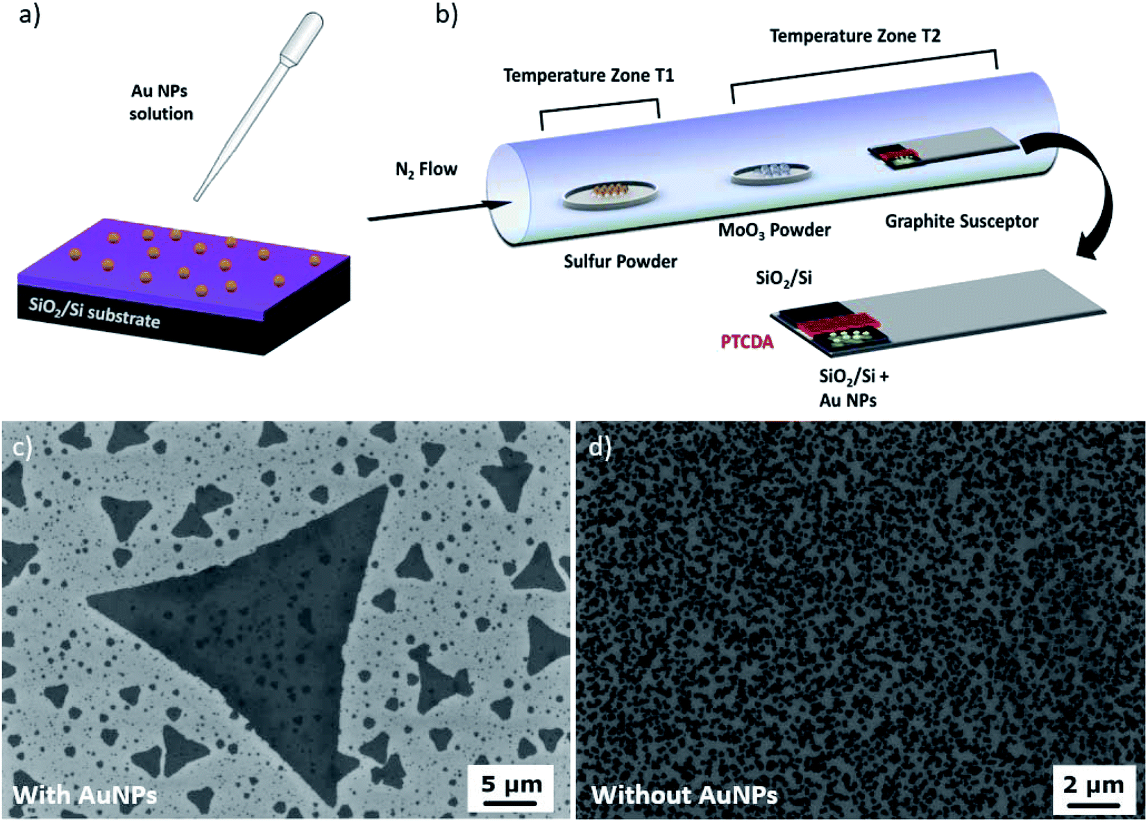 | ||
| Fig. 1 (a) Preparation of the gold nanoparticle coated SiO2/Si substrate (b) schematic of the CVD growth configuration. In the bottom panel we present the SEM images of MoS2 obtained with (c) and without (d) gold NPs. | ||
In Fig. 1b, we present the configuration of the growth system: one substrate with gold NPs and one without them were loaded on the graphite susceptor in a symmetrical position, with a Si piece with the PTCDA promoter in the middle. This configuration ensured that the two samples can be considered as grown under the same experimental conditions, allowing us to conclude that any difference between them can be attributed to the effect of gold NPs.
The sulfur temperature T1 was fixed at 140 °C, and the temperature of the powders and susceptor T2 was 785 °C. Temperature T1 was raised after T2 stabilized at 785 °C; during the heating time of sulfur, the nitrogen flow was inverted with respect to the arrow shown in Fig. 1, i.e. the gas was injected from the substrate side and flowed towards the sulfur boat. This switch allowed us to avoid any S and Mo prereaction during the temperature ramp, thus permitting a more precise control of the MoS2 nucleation.37
After 5 minutes of stabilization of T2, the nitrogen flow was reversed back and the growth commenced. As soon as the growth time was reached, all heaters were switched off and the system was let to cool down to room temperature under a nitrogen flow. Representative scanning electron microscopy (SEM) images of MoS2 synthesized with (Fig. 1c) and without (Fig. 1d) gold NPs show the beneficial effect of the employment of gold nanoparticles in the growth process in terms of the average lateral size of MoS2. The detailed characterization of MoS2 obtained without gold NPs is reported in Fig. S1.†
The use of gold nanoparticles results in the synthesis of MoS2 flakes with a large variety of lateral sizes, as shown in the SEM images in Fig. 2a. It is possible to consider three different families of flakes: irregular monolayer flakes with a lateral size in the range of hundreds of nm (1), triangular monolayer flakes with a micrometre size (2) and monolayer flakes with a lateral size of about 20 μm (3), although affected by adlayer islands. A high magnification SEM image (Fig. 2b) gives interesting insights into how gold NPs enhance the local growth of adlayer islands, as different metal nanoparticles are mainly found inside the islands. A similar effect has been already reported in the case of MoS2 synthesis assisted by metal seeds.28,29 It is worth noting that the adlayer islands with a lateral size of over 100 nm are mainly hexagonal (truncated triangles) shaped with a zero degree twisting with respect to the underlying flake, while islands, with 100 nm or lower size, are triangular with a 60° twisting. A statistical evaluation obtained from tens of SEM images reveals that 95% of the hexagonal shaped islands (average lateral size of 347 nm) are 0° rotated while 97% of the triangular islands (average lateral size of 84 nm) are 60° rotated with respect to the underlying MoS2 monolayer. The synthesis of MoS2 crystals with nanoparticles of different sizes and concentrations is presented in ESI Fig. S2 and S3.†
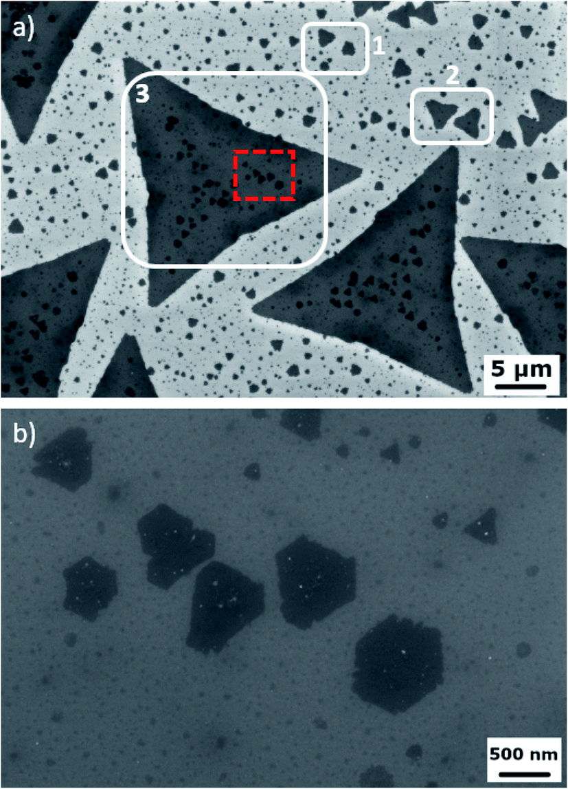 | ||
| Fig. 2 (a) SEM images of MoS2 flakes grown with gold NPs and (b) high magnification SEM images of the triangular and hexagonal adlayer islands highlighting the presence of residual nanoparticles. | ||
Elemental analysis of the metal nanoparticles was performed by Energy-dispersive X-ray spectroscopy (SEM-EDX) (Fig. 3) for studying the possible chemical reaction of the gold NPs during the growth process. The EDX spectra, shown in Fig. 3b, are acquired from different particles indicated by the colored arrows in the SEM image of Fig. 3a. In particular, the EDX spectra are acquired for ML-MoS2 (red line and arrow), for reference; a similar reference spectrum is acquired for the gold NP on the SiO2 substrate prior to the growth process (black line). The EDX spectra of gold NPs on ML MoS2 (green line and arrow) and of gold NPs on BL MoS2 (cyan line and arrow) are also reported. It has to be noted that in the latter spectra the molybdenum and sulfur signals are most likely screened by the presence of the gold nanoparticles. A comparison between the EDX spectra from different regions allows us to rule out a severe and extended alloying between gold and the growth precursors. However, a possible migration of gold over the flake area would lead to a doping effect which is below the sensitivity of the EDX technique and requires an accurate electrical characterization, as will be presented in the following section. The EDX spectra are reported on a larger scale (0–15 keV) in Fig. S4.†
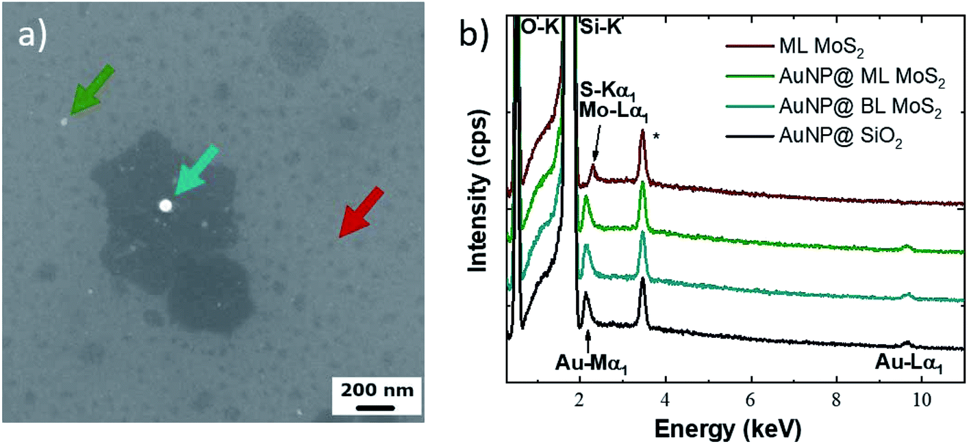 | ||
| Fig. 3 (a): SEM image where the arrows indicate the sites of the EDX spectra. (b) EDX spectra of ML MoS2 (red line), gold NPs on ML MoS2 (green line) and on BL MoS2 (cyan line) and the reference of gold NPs on the SiO2 substrate (black line), respectively. The asterisk indicates a peak due to the instrumental system. | ||
Fig. 4a shows a typical atomic force microscopy (AFM) image of a large MoS2 triangular flake, similar to the ones reported in the SEM image of Fig. 2a. The monolayer thickness is confirmed by the representative height scan line at the edge, shown in Fig. 4b. Furthermore, many adlayer islands are present on top of the large monolayer flake. A line profile of one of these adlayers is also reported in Fig. 4c, and the measured height is found to be compatible with a monolayer island residing on top of the monolayer flake. Finally, Fig. 4d shows the histogram of the height distribution obtained by statistical analysis of the adlayers, indicating that these consist of monolayer or bilayer islands. The nanoparticles at the edge are most likely due to the oxidation of ML MoS2.38,39
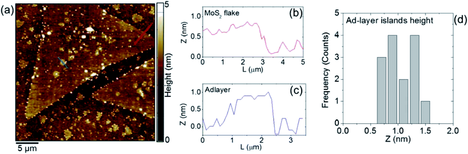 | ||
| Fig. 4 (a) AFM image of a large MoS2 triangular flake. (b) Height scan lines at the flake edge, confirming the monolayer thickness. (c) Height line profile of an adlayer island and (d) histogram of the adlayer height distribution. | ||
Raman spectroscopic mapping has been carried out in order to evaluate the exact number of MoS2 layers (Fig. 5). Fig. 5a shows the optical image of the flakes: the MoS2 flake shows a homogeneous optical contrast except for the darker contrast of the adlayer islands, indicating an increase in the number of MoS2 layers. In order to evaluate the exact number of layers, Fig. 5b shows the δ map, where δ is the separation between the A1g (out-of-plane vibration) and E2G (in-plane vibration) Raman modes.40,41 In the case of the MoS2 flake, we obtain δ = 19.3 cm−1, as indication for monolayer MoS2, while δ = 21.2 cm−1 is obtained in the case of the adlayer islands, suggesting bilayer islands. The E2G and A1G intensity maps are reported in Fig. S5 of the ESI†. The statistical analysis results of the maps are reported in Fig. 5c. The histogram shows that a bimodal distribution peaked at 18 cm−1 and 20 cm−1 with a tail on the high δ side. This analysis demonstrates that the flakes grown with gold NPs are composed mainly of ML and BL MoS2 with a small percentage of tri-layer islands. The representative Raman spectra of the MoS2 flake and the adlayer islands are reported in Fig. 5d. It is worth noting that the presence of gold nanoparticles in the adlayer islands, evidenced by SEM images, does not cause any strong enhancement of the intensity of the Raman modes, attributed to the effect of localized surface plasmon resonance (LSPR) of gold nanoparticles (i.e. surface-enhanced Raman scattering).32,42
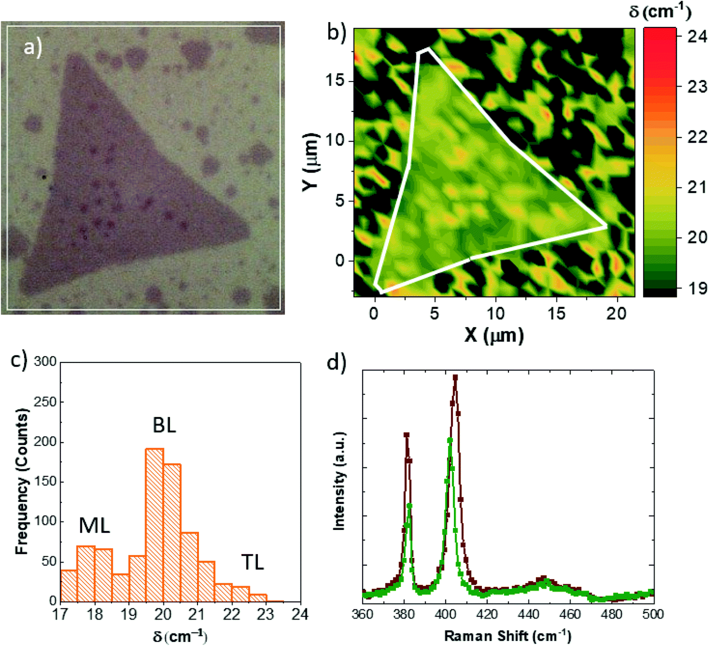 | ||
| Fig. 5 (a) Optical image of the MoS2 flake growth with gold nanoparticles, (b) Raman δ map, (c) statistical analysis of the mapping results and (d) representative Raman spectra of the underlying flake (green line) and of the islands (red line). | ||
The LSPR enhancement suppression is supported by the evaluation of the A1g/E2g intensity ratio, that decreases from 1.64 in the case of monolayer MoS2 to 1.3 in the case of adlayer islands.43
An additional insight is given by the different increases of the linewidth (FWHM) of the E2G and A1G modes; in fact in the case of ML MoS2, the linewidths are 2.9 cm−1 and 5.5 cm−1 for E2G and A1G, respectively, while they are 3.7 cm−1 and 6.2 cm−1 for the adlayer islands. The increase of the FWHM of both the Raman modes is an additional demonstration of the bilayer nature of such islands.40
On the basis of the above data, it can be argued that the growth mechanism is similar to the one of one dimensional nanostructures44,45 where the gold nanoparticles act as catalytic seeding points for the initial synthesis of the MoS2 monolayer. In Fig. 6, we present a schematic representation of our proposed interpretation of the growth process. After the deposition of gold nanoparticles (1), the substrate is inserted in the CVD system. During the heating ramp, the gold nanoparticles probably pin to the substrate. At the growth temperature, the substrate is exposed to the flow of Mo and S precursors, initially giving rise to the lateral growth of the MoS2 monolayer (2). Then, the size of the ML is increased (3) up to the merging in the 20 μm flakes with the concurrent appearance of the bilayer islands in correspondence with the gold nanoparticles (4). As nanometric gold nanoparticles favor the synthesis of bilayer MoS2 rather than the lateral synthesis of monolayer flakes, their lateral size appears to be limited to the 20 μm range.
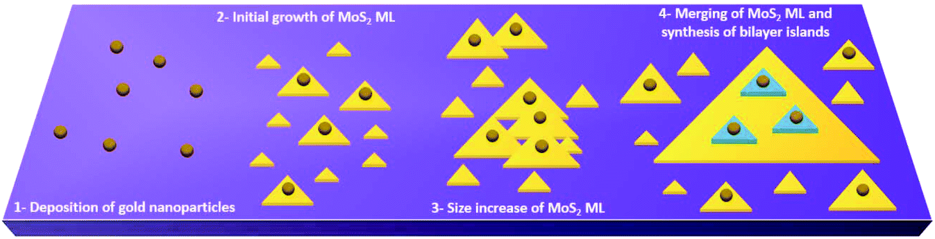 | ||
| Fig. 6 Schematic of the growth of MoS2 flakes assisted by gold nanoparticles. | ||
Fig. 7 shows the PL analysis of the same flake of Fig. 5. The A exciton PL intensity map is reported in Fig. 6a. The main result shows a strong inhomogeneity of the A exciton intensity, with some areas presenting a 50% quenching of the PL intensity.46 It is worth noting that the PL quenching is concurrent to a red-shift of the PL peak, reported in Fig. 7b. The A exciton peak shifts from 1.84 eV down to 1.82 eV. The quenching and red-shifted areas do not present a direct correlation with the presence of the adlayer islands. Therefore, the quenching can be due to residual gold nanoparticles in the monolayer area. In fact, a strong quenching in gold nanoparticles/MoS2 composites has been previously demonstrated.47,48
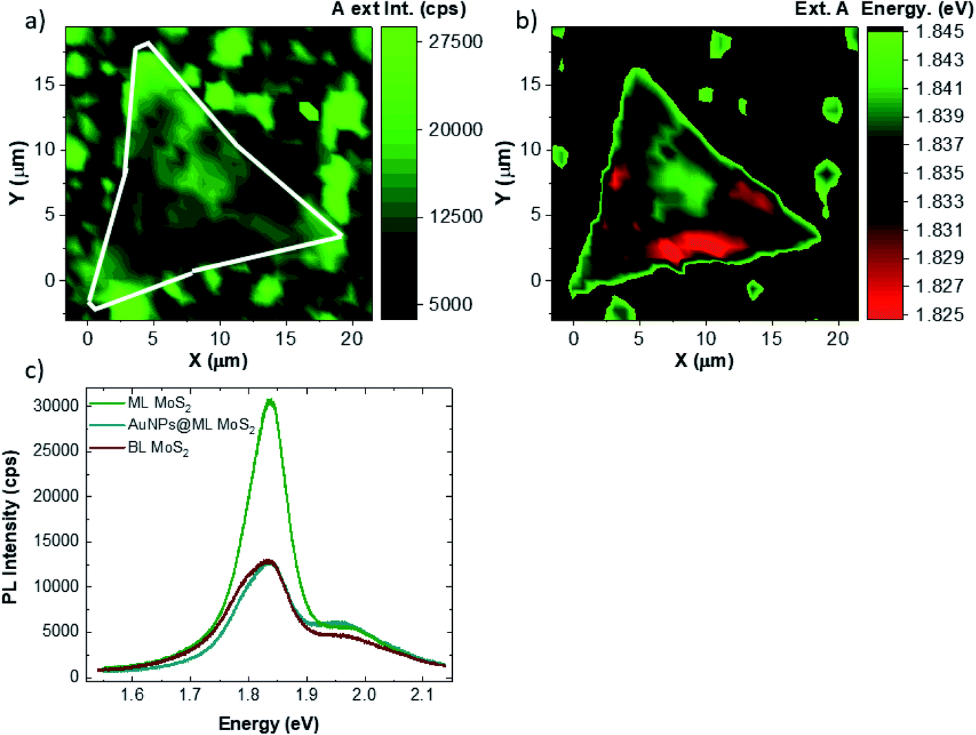 | ||
| Fig. 7 (a) PL map of the A exciton intensity, (b) PL map of the A exciton peak energy, (c) representative PL spectra of ML MoS2 (green line), of gold NP coupled ML MoS2 (cyan line) and of the BL island (red line). | ||
In order to gain more insights, we carried out PL spectroscopy on three different areas: ML MoS2 (green line), gold NP coupled ML MoS2 (cyan line) and BL MoS2 (red line). The PL spectra can be deconvolved into three Voight peaks, as reported in Fig. S6.† The peaks at 1.78 eV, 1.84 eV and 1.98 eV can be attributed to the trion, A exciton and B exciton emissions, respectively.46,49 All the parameters of the fitting are reported in Tables S1, S2 and S3.† The main difference between the ML and BL MoS2 spectra is the decrease of the integrated intensity of the A exciton by 59%, while the trion and the B exciton intensities are only slightly decreased by 6% and 21%, respectively. It is worth noting that between ML and BL MoS2, the emissions are peaked at the same energy and similar linewidth. Instead, if we compare the PL spectra of ML MoS2 and gold NP coupled ML MoS2, the B exciton is slightly red-shifted from 1.98 eV down to 1.95 eV when the ML is coupled with the metal nanostructures, while the trion and A exciton are peaked at the same energy in both cases. A comparison of the integrated intensities reveals that in the case of gold NP coupled ML MoS2, the intensities of trion and of A exciton are decreased by 17% and 78% while the integrated intensity of the B exciton is similar.
Finally, the electrical characterization of monolayer MoS2 flakes grown by gold NP assisted CVD was carried out using back-gated field effect transistors (FETs) as test devices. Fig. 8a shows the output characteristics (ID–VDS for gate bias VG ranging from 0 to 20 V) measured on a FET with a channel length L = 10 μm. A linear behavior at low drain bias, followed by current saturation at higher bias can be observed, indicating a good electrostatic control of the MoS2 channel. The transfer characteristics ID−VG of the transistor at VDS = 1 V are reported in Fig. 8b. By fitting the linear region of this curve, the field effect mobility (μ ≈ 1 cm2 V−1 s−1) was obtained from the slope (gm/W = 1.12 × 10⁻⁹ S μm−1), according to the relation 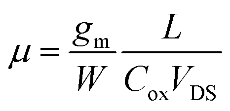 , with Cox = 11.9 nF cm−2 being the capacitance per unit area of the 290 nm thick SiO2 gate oxide. Furthermore, the threshold voltage Vth = 4.9 V was evaluated as the intercept with the ID = 0 axis. It is noteworthy that a positive threshold voltage is obtained for these backgated transistors fabricated with MoS2 grown using gold NP assisted CVD. There is a remarkable difference with respect to transistors fabricated using similar geometry and the same SiO2 thickness on CVD grown MoS2 without gold nanoparticles,50 which showed a negative threshold voltage (Vth = −20 V).
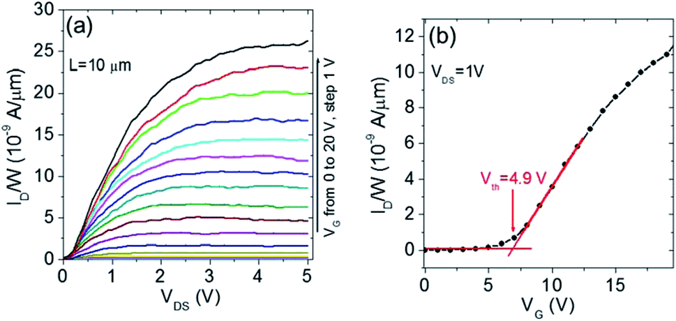 | ||
| Fig. 8 (a) Output characteristics ID–VDS measured on a backgated FET with a monolayer MoS2 channel (CVD grown with gold NPs). (b) Transfer characteristics of the device, from which the threshold voltage (Vth = 4.9 V) was estimated. | ||
Similar positive shifts of the threshold voltage have been recently reported by other authors in backgated transistors with the monolayer MoS2 channel functionalized by gold via S–Au–Cl coordination complexes.33 This phenomenon was explained in terms of a fixed charge QF on the channel associated to the AuCl complexes coordinated to the S atoms. Analogous effects can be ascribed to the gold nanoparticle functionalization of the MoS2 layer during CVD growth aided by gold nanoparticles.51,52 A p-type doping of MoS2 of 1.85 × 1012 cm−2 was estimated from the difference of the threshold voltages (ΔVth = 24.9 V) measured on FET devices fabricated with MoS2 flakes grown with and without AuNPs, according to the equation p = CoxΔVth/q, where q is the electron charge.
These results are of particular interest, as they show that the use of gold NPs as seeds for MoS2 results in a positive threshold in FETs. This is a desirable feature in these devices, as it allows us to have transistors with no current flowing when the gate voltage is zero, with positive effects both for energy efficiency and for safety. On the other hand, values of mobility of these FETs are lower than those commonly reported, indicating that some work on optimization of these nanostructures for electronic applications is still needed.
Conclusions
In conclusion, we have presented a complete study of the CVD-based synthesis of ML MoS2 assisted by gold nanoparticles.We show that nanoparticle assisted CVD synthesis improves the lateral size of MoS2 monolayers, allowing them to reach an average size of 20 μm, although they are affected by nanometric bilayer islands. Compositional-sensitive characterization indicates that gold nanoparticles are preserved during the CVD growth and are mostly found in MoS2 islands. Optical characterization highlighted that the presence of gold nanoparticles causes a quenching of the A exciton PL emission and a suppression of the LSPR enhancement.
On the other hand, a study of the electrical properties of these nanostructures showed that the employment of gold nanoparticles during the growth process results in a positive shift of the threshold voltage in back-gated FETs, due to the presence of an additional fixed charge in the FET channel. To summarize our experimental findings, the deposition of gold NPs prior to CVD growth of 2D layers of MoS2 results in: (i) an improvement of the lateral growth of flakes, (ii) a quenching of the A exciton PL emission of flakes, and (iii) a positive value of the threshold voltage in back-gated FETs.
We conclude that the use of gold NPs has the potential to allow the control of the flake position, paving the way for an efficient deterministic synthesis of layered materials in comparison to lithographic metal seeding without the issue of a bulk-like material in proximity of the metal seeds.
Methods
We used two different SEM microscopes; for morphological characterization, SEM analysis was carried out using an in-lens detector in a Zeiss Merlin FEG-SEM microscope, with an accelerating voltage of 5 kV and an electron current of 12 pA, in order to minimize the damage due to the electron beam irradiation, while energy dispersive X-ray (EDX) spectroscopy was performed on a Zeiss SUPRA40 FEG-SEM with a GEMINI column, equipped with an Oxford Instruments EDX microanalysis setup. The elemental analysis was performed at an accelerating voltage of 20 kV, to be able to excite the L lines of gold.AFM topography was performed using a PSIA XE100 AFM operated in the non-contact mode by using Si tips with ∼5 nm curvature radius.
Scanning Raman and photoluminescence (PL) spectroscopy was carried out with a Renishaw InVia system, equipped with a confocal microscope, a 532 nm excitation laser and a 1800 line per mm grating (spectral resolution 2 cm−1). All the analyses were performed with a 100× objective (NA = 0.85), excitation laser power of 500 μW, four seconds of acquisition time for each spectrum and pixel size of 1 μm × 1 μm.
MoS2 FETs (with the SiO2/p+-Si substrate working as the backgate) were fabricated by the deposition of the source/drain ohmic contacts, consisting of a Ni(20 nm)/Au(100 nm) double layer, onto lithographically defined MoS2 areas. The electrical characteristics of these devices were measured in a CASCADE Microtech probe station, using an Agilent 4156b parameter analyzer.
Conflicts of interest
There are no conflicts to declare.Acknowledgements
We thank Dr Laura Lazzarini of IMEM-CNR for fruitful scientific discussions, and S. Di Franco from IMM-CNR for the expert assistance in device fabrication.References
- A. Splendiani, L. Sun, Y. Zhang, T. Li, J. Kim, C. Y. Chim, G. Galli and F. Wang, Nano Lett., 2010, 10, 1271–1275 CrossRef CAS PubMed.
- K. F. Mak, C. Lee, J. Hone, J. Shan and T. F. Heinz, Phys. Rev. Lett., 2010, 105, 136805 CrossRef PubMed.
- K. F. Mak and J. Shan, Nat. Photonics, 2016, 10, 216–226 CrossRef CAS.
- X. Liu, T. Galfsky, Z. Sun, F. Xia, E. Lin, Y.-H. Lee, S. Kéna-Cohen and V. M. Menon, Nat. Photonics, 2015, 9, 30–34 CrossRef CAS.
- M. Negri, L. Francaviglia, D. Dumcenco, M. Bosi, D. Kaplan, V. Swaminathan, G. Salviati, A. Kis, F. Fabbri and A. Fontcuberta i Morral, Nano Lett., 2019, 20, 567–576 CrossRef PubMed.
- S. Ghatak, A. N. Pal and A. Ghosh, ACS Nano, 2011, 5, 7707–7712 CrossRef CAS PubMed.
- G. Migliato Marega, Y. Zhao, A. Avsar, Z. Wang, M. Tripathi, A. Radenovic and A. Kis, Nature, 2020, 587, 72–77 CrossRef CAS PubMed.
- S. Conti, L. Pimpolari, G. Calabrese, R. Worsley, S. Majee, D. K. Polyushkin, M. Paur, S. Pace, D. H. Keum, F. Fabbri, G. Iannaccone, M. Macucci, C. Coletti, T. Mueller, C. Casiraghi and G. Fiori, Nat. Commun., 2020, 11, 3566 CrossRef CAS PubMed.
- C.-H. Yeh, Z.-Y. Liang, Y.-C. Lin, H.-C. Chen, T. Fan, C.-H. Ma, Y.-H. Chu, K. Suenaga and P.-W. Chiu, ACS Nano, 2020, 14, 985–992 CrossRef CAS PubMed.
- H. Wang, L. Yu, Y.-H. Lee, Y. Shi, A. Hsu, M. L. Chin, L.-J. Li, M. Dubey, J. Kong and T. Palacios, Nano Lett., 2012, 12, 4674–4680 CrossRef CAS PubMed.
- Q. H. Wang, K. Kalantar-Zadeh, A. Kis, J. N. Coleman and M. S. Strano, Nat. Nanotechnol., 2012, 7, 699–712 CrossRef CAS PubMed.
- B. Radisavljevic and A. Kis, Nat. Mater., 2013, 12, 815–820 CrossRef CAS PubMed.
- B. Radisavljevic, M. B. Whitwick and A. Kis, ACS Nano, 2011, 5, 9934–9938 CrossRef CAS PubMed.
- H. S. Lee, S.-W. Min, Y.-G. Chang, M. K. Park, T. Nam, H. Kim, J. H. Kim, S. Ryu and S. Im, Nano Lett., 2012, 12, 3695–3700 CrossRef CAS PubMed.
- C. Huyghebaert, T. Schram, Q. Smets, T. K. Agarwal, D. Verreck, S. Brems, A. Phommahaxay, D. Chiappe, S. El Kazzi, C. L. de la Rosa, G. Arutchelvan, D. Cott, J. Ludwig, A. Gaur, S. Sutar, A. Leonhardt, D. Marinov, D. Lin, M. Caymax, I. Asselberghs, G. Pourtois and I. P. Radu, in, IEEE International Electron Devices Meeting, IEDM, 2018, pp. 22.1.1–22.1.4 Search PubMed.
- S. Manzeli, D. Ovchinnikov, D. Pasquier, O. V. Yazyev and A. Kis, Nat. Rev. Mater., 2017, 2, 17033 CrossRef CAS.
- M. Bosi, RSC Adv., 2015, 5, 75500–75518 RSC.
- D. Dumcenco, D. Ovchinnikov, K. Marinov, P. Lazić, M. Gibertini, N. Marzari, O. L. Sanchez, Y. C. Kung, D. Krasnozhon, M. W. Chen, S. Bertolazzi, P. Gillet, A. Fontcuberta I Morral, A. Radenovic and A. Kis, ACS Nano, 2015, 9, 4611–4620 CrossRef CAS PubMed.
- Y. Zhan, Z. Liu, S. Najmaei, P. M. Ajayan and J. Lou, Small, 2012, 8, 966–971 CrossRef CAS PubMed.
- Y.-H. Lee, X.-Q. Zhang, W. Zhang, M.-T. Chang, C.-T. Lin, K.-D. Chang, Y.-C. Yu, J. T.-W. Wang, C.-S. Chang, L.-J. Li and T.-W. Lin, Adv. Mater., 2012, 24, 2320–2325 CrossRef CAS PubMed.
- T. Schram, Q. Smets, B. Groven, M. H. Heyne, E. Kunnen, A. Thiam, K. Devriendt, A. Delabie, D. Lin, M. Lux, D. Chiappe, I. Asselberghs, S. Brus, C. Huyghebaert, S. Sayan, A. Juncker, M. Caymax and I. P. Radu, in European Solid-State Device Research Conference, Editions Frontieres, 2017, pp. 212–215 Search PubMed.
- A. Kozhakhmetov, J. Nasr, F. Zhang, K. Xu, N. Briggs, R. Addou, R. M. Wallace, S. K. Fullerton-Shirey, M. Terrones, S. Das and J. A. Robinson, 2D Mater., 2020, 7, 015029 CrossRef CAS.
- S. Pace, M. Ferrera, D. Convertino, G. Piccinini, M. Magnozzi, N. Mishra, S. Forti, F. Bisio, M. Canepa, F. Fabbri and C. Coletti, arXiv, 2020.
- G. H. Han, N. J. Kybert, C. H. Naylor, B. S. Lee, J. Ping, J. H. Park, J. Kang, S. Y. Lee, Y. H. Lee, R. Agarwal and A. T. C. Johnson, Nat. Commun., 2015, 6, 6128 CrossRef CAS PubMed.
- A. Sharma, R. Mahlouji, L. Wu, M. A. Verheijen, V. Vandalon, S. Balasubramanyam, J. P. Hofmann, W. M. M. Kessels and A. A. Bol, Nanotechnology, 2020, 31, 255603 CrossRef CAS PubMed.
- X. Wang, K. Kang, S. Chen, R. Du and E.-H. Yang, 2D Mater., 2017, 4, 25093 CrossRef.
- P. K. Mohapatra, K. Ranganathan and A. Ismach, Adv. Mater. Interfaces, 2020, 7, 2001549 CrossRef CAS.
- Y. Li, S. Hao, J. G. DiStefano, A. A. Murthy, E. D. Hanson, Y. Xu, C. Wolverton, X. Chen and V. P. Dravid, ACS Nano, 2018, 12, 8970–8976 CrossRef CAS PubMed.
- Z. Wang, Q. Huang, P. Chen, S. Guo, X. Liu, X. Liang and L. Wang, Sci. Rep., 2016, 6, 38394 CrossRef CAS PubMed.
- A. Patsha, V. Sheff and A. Ismach, Nanoscale, 2019, 11, 22493–22503 RSC.
- Y. Li, M. B. Majewski, S. M. Islam, S. Hao, A. A. Murthy, J. G. DiStefano, E. D. Hanson, Y. Xu, C. Wolverton, M. G. Kanatzidis, M. R. Wasielewski, X. Chen and V. P. Dravid, Nano Lett., 2018, 18, 7104–7110 CrossRef CAS PubMed.
- Y. Li, J. D. Cain, E. D. Hanson, A. A. Murthy, S. Hao, F. Shi, Q. Li, C. Wolverton, X. Chen and V. P. Dravid, Nano Lett., 2016, 16, 7696–7702 CrossRef CAS PubMed.
- H. Liu, D. Grasseschi, A. Dodda, K. Fujisawa, D. Olson, E. Kahn, F. Zhang, T. Zhang, Y. Lei, R. B. N. Branco, A. L. Elías, R. C. Silva, Y.-T. Yeh, C. M. Maroneze, L. Seixas, P. Hopkins, S. Das, C. J. S. de Matos and M. Terrones, Sci. Adv., 2020, 6, eabc9308 CrossRef CAS PubMed.
- E. Rotunno, M. Bosi, L. Seravalli, G. Salviati and F. Fabbri, Nanoscale Adv., 2020, 2, 2352–2362 RSC.
- X. Ling, Y. H. Lee, Y. Lin, W. Fang, L. Yu, M. S. Dresselhaus and J. Kong, Nano Lett., 2014, 14, 464–472 CrossRef CAS PubMed.
- L. Seravalli, M. Bosi, S. Beretta, F. Rossi, D. Bersani, N. Musayeva and C. Ferrari, Nanotechnology, 2019, 30, 415603 CrossRef CAS PubMed.
- J. Chen, W. Tang, B. Tian, B. Liu, X. Zhao, Y. Liu, T. Ren, W. Liu, D. Geng, H. Y. Jeong, H. S. Shin, W. Zhou and K. P. Loh, Adv. Sci., 2016, 3, 1500033 CrossRef PubMed.
- Y. Okuno, O. Lancry, A. Tempez, C. Cairone, M. Bosi, F. Fabbri and M. Chaigneau, Nanoscale, 2018, 10, 14055–14059 RSC.
- F. Fabbri, F. Dinelli, S. Forti, L. Sementa, S. Pace, G. Piccinini, A. Fortunelli, C. Coletti and P. Pingue, J. Phys. Chem. C, 2020, 124, 9035–9044 CrossRef CAS.
- C. Lee, H. Yan, L. E. Brus, T. F. Heinz, J. Hone and S. Ryu, ACS Nano, 2010, 4, 2695–2700 CrossRef CAS PubMed.
- R. Ganatra and Q. Zhang, ACS Nano, 2014, 8, 4074–4099 CrossRef CAS PubMed.
- S. Zu, B. Li, Y. Gong, Z. Li, P. M. Ajayan and Z. Fang, Adv. Opt. Mater., 2016, 4, 1463–1469 CrossRef CAS.
- J. Shakya, A. S. Patel, F. Singh and T. Mohanty, Appl. Phys. Lett., 2016, 108, 13103 CrossRef.
- C. Jia, Z. Lin, Y. Huang and X. Duan, Chem. Rev., 2019, 119, 9074–9135 CrossRef CAS PubMed.
- M. Bosi, L. Seravalli, S. Beretta and C. Ferrari, Nanotechnology, 2019, 30, 084002 CrossRef CAS PubMed.
- T. Goswami, R. Rani, K. S. Hazra and H. N. Ghosh, J. Phys. Chem. Lett., 2019, 10, 3057–3063 CrossRef CAS PubMed.
- U. Bhanu, M. R. Islam, L. Tetard and S. I. Khondaker, Sci. Rep., 2014, 4, 5575 CrossRef CAS PubMed.
- J. Yan, C. Ma, P. Liu and G. Yang, ACS Photonics, 2017, 4, 1092–1100 CrossRef CAS.
- S. Golovynskyi, I. Irfan, M. Bosi, L. Seravalli, O. I. Datsenko, I. Golovynska, B. Li, D. Lin and J. Qu, Appl. Surf. Sci., 2020, 515, 146033 CrossRef CAS.
- F. Giannazzo, M. Bosi, F. Fabbri, E. Schilirò, G. Greco and F. Roccaforte, Phys. Status Solidi RRL, 2020, 14, 1900393 CrossRef CAS.
- A. K. Singh, R. K. Pandey, R. Prakash and J. Eom, Appl. Surf. Sci., 2018, 437, 70–74 CrossRef CAS.
- Y. Shi, J.-K. Huang, L. Jin, Y.-T. Hsu, S. F. Yu, L.-J. Li and H. Y. Yang, Sci. Rep., 2013, 3, 1839 CrossRef PubMed.
Footnote |
| † Electronic supplementary information (ESI) available. See DOI: 10.1039/d1na00367d |
| This journal is © The Royal Society of Chemistry 2021 |