
 Open Access Article
 This Open Access Article is licensed under a Creative Commons Attribution-Non Commercial 3.0 Unported Licence
Controlled self-assembly of block copolymers in printed sub-20 nm cross-bar structures†
Tae Wan
Park
 ab,
Young Lim
Kang
c,
Myunghwan
Byun
d,
Suck Won
Hong
e,
Yong-Sik
Ahn
c,
Junghoon
Lee
*f and
Woon Ik
Park
*c
ab,
Young Lim
Kang
c,
Myunghwan
Byun
d,
Suck Won
Hong
e,
Yong-Sik
Ahn
c,
Junghoon
Lee
*f and
Woon Ik
Park
*c
aElectronic Convergence Materials Division, Korea Institute of Ceramic Engineering & Technology (KICET), 101 Soho-ro, Jinju 52851, Republic of Korea
bDepartment of Materials Science and Engineering, Korea University, Seoul 02841, Republic of Korea
cDepartment of Materials Science and Engineering, Pukyoung National University (PKNU), 45 Yongso-ro, Nam-gu, Busan 48513, Republic of Korea. E-mail: thane0428@pknu.ac.kr
dDepartment of Advanced Materials Engineering, Keimyung University, 1095 Dalgubeol-daero, Daegu 42601, Republic of Korea
eDepartment of Cogno-Mechatronics Engineering, Department of Optics and Mechatronics Engineering, College of Nanoscience and Nanotechnology, Pusan National University, Busan 46241, Republic of Korea
fDepartment of Metallurgical Engineering, Pukyoung National University (PKNU), 45 Yongso-ro, Nam-gu, Busan 48513, Republic of Korea. E-mail: jlee1@pknu.ac.kr
First published on 2nd August 2021
Abstract
Directed self-assembly (DSA) of block copolymers (BCPs) has garnered much attention due to its excellent pattern resolution, simple process, and good compatibility with many other lithography methods for useful nanodevice applications. Here, we present a BCP-based multiple nanopatterning process to achieve three-dimensional (3D) pattern formation of metal/oxide hybrid nanostructures. We employed a self-assembled sub-20 nm SiOx line pattern as a master mold for nanotransfer printing (nTP) to generate a cross-bar array. By using the transfer-printed cross-bar structures as BCP-guiding templates, we can obtain well-ordered BCP microdomains in the distinct spaces of the nanotemplates through a confined BCP self-assembly process. We also demonstrate the morphological evolution of a cylinder-forming BCP by controlling the BCP film thickness, showing a clear morphological transition from cylinders to spheres in the designated nanospaces. Furthermore, we demonstrate how to control the number of BCP spheres within the cross-bar 3D pattern by adjusting the printing angle of the multiple nTP process to provide a suitable area for spontaneous BCP accommodation. This multiple-patterning-based approach is applicable to useful 3D nanofabrication of various devices with complex hybrid nanostructures.
Introduction
For the past several decades, the directed self-assembly (DSA) of block copolymers (BCPs) has been widely studied as a promising candidate for next-generation lithography due to its excellent pattern resolution, process simplicity, and useful nanoscale fabrication with high-density.1–7 Particularly, BCPs with a high Flory–Huggins interaction parameter (χ) can produce various highly ordered sub-20 nm nanostructures, such as spheres, cylinders, hexagonally perforated lamellae (HPL), and lamellae, through a microphase separation process.8–12 Furthermore, high-χ BCPs spontaneously self-assemble into nanostructures with a low defect density and excellent line edge roughness, compared to low-χ BCPs, according to previous studies.13 For these reasons, many BCP research groups have investigated advanced self-assembly technologies to engineer various high-χ BCPs, demonstrating the effective formation of periodic two-dimensional (2D) planar patterns.14,15To extend the versatility of BCP structures further, several other groups who study BCPs have suggested innovative BCP-manipulation methods to generate a variety of complex and unique 3D nanostructures.16–20 In particular, Tavakkoli et al. demonstrated how to obtain bi-layered 3D BCP morphologies by using a post array for which the surface was modified with a brush attractive to the majority block of the di-BCP.21 They showed a rich variety of 3D nanostructures consisting of line structures with controllable angles, bends, and junctions by adjusting the height and chemical preferences of nano-post templates. Onses et al. introduced a high-resolution jet printing technique to obtain hierarchical 3D BCP patterns over a large area through electrohydrodynamic effects.22 They demonstrated the jet-printed pattern generation of BCPs with well-organized feature sizes, good periodicities and complex geometries by thermal annealing, in overall layouts consisting of various patterns with a wide range of feature sizes from the nanoscale to the macroscale. Also, Subramanian et al. presented a templated 3D ZnO cross-bar structure directly derived from hierarchically self-assembled 3D BCP thin films.23 They presented well-ordered ZnO nanodevices created by selective infiltration synthesis in microphase-separated BCP patterns that showed excellent electrical functionalities. Other BCP groups also reported examples of the successful pattern creation of unusual 3D BCP geometries, including self-assembled 3D gyroid BCP structures for optical metamaterials.24–28 These results clearly show the promising potential of directly self-assembled 3D BCPs and the importance of BCP-based patterning technologies.
As another strategy for complex 2D and/or useful 3D nanofabrication, the nano-transfer printing (nTP) method has attracted considerable attention due to its simple and high-throughput process achievable at a low cost.29–33 Several nTP research groups have reported useful nTP methods, showing that it is possible reliably to create well-ordered nano-to-micro patterns with precision by transfer printing onto target substrates with the help of elastomeric soft molds with low surface energy.34–36 For example, Zaumseil et al. presented a simple nTP process to obtain complex 2D and 3D functional patterns over a large area by using elastomeric polydimethylsiloxane (PDMS) stamps.37 Hwang et al. demonstrated a liquid-bridge nTP process capable of forming ultrafine nanostructures on a four-inch wafer, demonstrating the successful fabrication of nanowire field-effect transistors and arrays of pentacene thin-film transistors.38 Wie et al. also showed a wafer-recyclable, environmentally friendly nTP method to deliver thin-film nanoelectronics entirely with complex circuits by wafer-scale delamination in a water environment at room temperature.39 Very recently, we also demonstrated an innovative thermally assisted nTP (T-nTP) technique that easily generates various nanostructures on rigid and/or flexible target substrates at the eight-inch wafer scale using a laminator capable of providing uniform pressure and heat.40 The reliable patterning of various high-resolution features was achieved by employing a self-assembled sub-20 nm SiOx master mold, resulting in an ultrafine 3D cross-bar array of NiOx/Pt resistive memory. Despite these efforts to improve the nTP process, however, various nTP methods remain limited in terms of their ability to form sub-20 nm hybrid 3D pattern geometries. Therefore, it is very important to develop more facile and useful sub-20 nm patterning methods capable of effectively obtaining complex hybrid nanopatterns for functional nanodevice applications.
Here, we demonstrate a unique multiple-patterning method consisting of an nTP process and the DSA of the BCP for the creation of reliable 3D patterns of unusual metal–oxide hybrid nanoscale structures. First, we show how to obtain cross-bar nanostructures using a self-assembled master mold of sub-20 nm SiOx lines based on the nTP process. We also present well-organized BCP spherical domains in the transfer-printed nanospaces of the cross-bar template through the confined microphase-separation of high-χ BCPs. In addition, we display a reliable morphology transition from cylinders to spheres at specific positions of the metal cross-bar array by controlling the film thickness of the BCP. Moreover, we present a controlled number of BCP spheres within the modified cross-bar spaces through a confined BCP self-assembly process that involves manipulating the printing angle when repeating the nTP process.
Experimental
BCP self-assembly: SiOx master mold
A cylinder-forming poly(styrene-b-dimethylsiloxane) (PS-b-PDMS) BCP (SD45, χ = ∼0.26) with a molecular weight (MW) of 45 kg mol−1 and a minority PDMS volume fraction (fPDMS) of ∼33.7% was purchased from Polymer Source Inc. The SD45 BCP powder was dissolved in a good solvent (toluene) of SD45, yielding a 1.0 wt% solution. After spin-casting the BCP solution onto the topographically patterned Si substrate fabricated by conventional KrF photolithography followed by a reactive ion etching (RIE) process, the BCP film was thermally annealed in toluene at 85 °C for 90 min. The annealed SD45 thin film was then etched with CF4 plasma (50 W, 25 s) followed by O2 plasma (60 W, 35 s) at 10 mTorr to remove the top-PDMS layer and PS matrix, respectively, resulting in periodic oxidized PDMS (SiOx) line structures with a width of 16 nm.Nanotransfer printing (nTP)
The self-assembled SiOx line-shaped master mold was initially surface-modified with a hydroxy-terminated PDMS brush (5 kg mol−1, Polymer Source Inc.) for easy separation from the sub-20 nm SiOx mold. After a replica material of PMMA (MW = 100 kg mol−1) was dissolved in a binary solvent of toluene and acetone at 4 wt%, the PMMA solution was spin-coated onto the SiOx master mold followed by duplication with an adhesive PI film (3M Inc.), resulting in the high-resolution PMMA replica structure. To transfer periodic Al cross-bar nanostructures, we employed a T-nTP process with a simple laminating system (LAMIART-470 LSI, GMP Corp.) to provide uniform heat and pressure. After sputter-deposition of the Al material onto the replica pattern, the Al pattern was transfer-printed onto the target Si substrate at the optimum temperature of 150 °C and under mild pressure (∼25 kPa). The cross-bar pattern was obtained by repeating the nTP process twice with different printing angles.BCP self-assembly: metal/oxide 3D hybrid structure
We used two PS-b-PDMS BCPs of cylinder-forming SD16 with a MW of 16 kg mol−1 and sphere-forming SD28 with a MW of 28 kg mol−1 to generate metal/oxide 3D hybrid nanostructures. The BCP self-assembly process was conducted on the printed Al cross-bar arrays. All complex nanostructures of line-in-mesh, dot-in-mesh, and double dots-in-mesh structures were obtained after a RIE process.Characterization
All 2D and 3D images of the nanostructures were observed using a field emission scanning electron microscope (FE-SEM, TESCAN MIRA3) operated with an acceleration voltage of 10 kV and working distance of 3.5–5 mm.Results and discussion
Controlled SiOx nanostructures by printed cross-bar templates
Fig. 1 shows the procedure to generate various metal–oxide hybrid 3D nanostructures consisting of cross-bar metal and self-assembled SiOx structures. Complex sub-20 nm 3D pattern geometries can be obtained by combining the nanopatterning method of the nTP process and the DSA of BCP. Specifically, the self-assembled BCP morphology on the nanomesh structure can be controlled by the BCP film thickness and/or printed template shape. Fig. 1a shows two different BCP morphologies of self-assembled cylinders and spheres in a cross-bar array depending on the BCP film thickness. First, we obtain a highly ordered SiOx line structure within a guiding Si template via the conventional DSA process of the SD45 BCP, as shown in Fig. S1 of the ESI.† Then, we employ the self-assembled SiOx line structure as a mold to fabricate a sub-20 nm metallic mesh structure through a twice-run nTP process. The printing alignment of the multi-stacked metal cross-bar template is manually controlled using a protractor and ruler. While the SiOx line structure is obtained at a relatively thick film from the cylinder-forming PS-b-PDMS BCP on the metal nanomesh, SiOx dot patterns are formed in the space of the cross-bar template through the confinement of spherical PDMS microdomains under the optimum thickness condition of the thin BCP film. In general, a cylinder-forming BCP generates a line structure, because the BCP morphology depends on the volume fraction of the BCP at an equilibrium state. However, if the film thickness of the BCP is ultra-thin, a meta-stable dot structure can be formed. Fig. 1b shows controlled SiOx nanodot patterns in cross-bar metal structures with two different printing angles of 90° and 60°, when using a sphere-forming PS-b-PDMS BCP. Self-assembled single SiOx dots are positioned in each nanospace of the cross-bar array with an angle of 90°, whereas double SiOx dots are located in the diamond-shaped space of the cross-bar template with an angle of 60°. | ||
| Fig. 1 Procedure for the formation of various self-assembled SiOx nanostructures within printed cross-bar metal templates. (a) Thickness dependency of the cylinder-forming PS-b-PDMS BCP morphology in a cross-bar array. (b) Controlled SiOx nanodot patterns of the sphere-forming PS-b-PDMS BCP on cross-bar templates with printing angles of 90° and 60°. | ||
Pattern formation of the line-in-mesh hybrid 3D nanostructure
Nanopatterning of multi-stacked hybrid 3D structures consisting of more than two materials is very important to diversify the pattern geometries with functionalities applicable to a wide range of device applications. As another strategy to extend the versatility of the T-nTP process, multiple lithography methods consisting of two different nanopatterning processes based on BCP self-assembly can be used to create functional hybrid nanostructures with various pattern geometries. Specifically, twice BCP self-assembly processes are needed: (1) fabrication of a sub-20 nm SiOx line mold for the nTP process, and (2) pattern generation of a sub-10 nm SiOx line structure in the printed cross-bar array by nTP. In general, cylinder-forming BCPs are self-assembled into line-shaped nanostructures. Fig. 2a presents a morphological comparison of the self-assembled cylinder-forming SD16 BCP with and without the guiding template. While a poorly ordered SiOx line pattern was formed on a planar bare-Si substrate, a highly ordered sub-10 nm SiOx line structure was produced in a topographical Si template. This is one of the typical template-based DSA processes of BCPs. For the successful generation of a line-in-mesh hybrid 3D pattern consisting of an oxide and a metal, we employed a combined nanopatterning method of nTP and DSA of the BCP. In other words, periodic sub-10 nm SiOx lines can be self-assembled within a 3D mesh structure formed by nTP through the specific microphase-separation of the SD16 BCP. A cross-bar metallic template can be obtained from the self-assembled SiOx SD45 line mold with a width of 16 nm through the twice-run nTP process, as shown in Fig. 2b. Fig. 2c shows a well-defined 1D-in-3D structure of a sub-10 nm SiOx line pattern templated by a printed Al cross-bar array after the self-assembly process of the SD16 BCP on an Al template. The hybrid oxide/metal 3D structure is composed of four regions, line-on-mesh, line-in-line, Al line, and no pattern, resulting from the self-assembled nTP SiOx mold in the patterned guiding Si template. In the case of the line-on-mesh structure, the SiOx lines may also be observed under the upper metal lines if the cross-bar structure consisting of metal lines with a higher dimension is used as a guiding template. Here, it should be noted that the combined patterning method of nTP and DSA of the BCP can effectively enhance the diversity of 3D nanopattern geometries.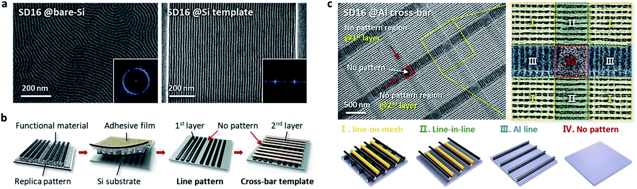 | ||
| Fig. 2 Comparison of the self-assembled cylinder-forming SD16 BCP with/without guiding templates. (a) Self-assembled sub-10 nm SiOx line structures on (left) a planar bare-Si substrate and (right) a topographical guiding Si template. The inset images show fast Fourier transform (FFT) patterns, indicating the (left) disordering and (right) ordering of the self-assembled SD16 BCP morphologies. (b) Procedure for the formation of the cross-bar nanotemplate through a twice-run n-TP process on a bare-Si substrate. (c) Self-assembled sub-10 nm SiOx line structure templated by the printed Al cross-bar pattern. The hybrid SiOx lines in the Al cross-bar array are composed of four regions: (I) line-on-mesh, (II) line-in-line, (III) Al line, and (IV) no pattern. | ||
Thickness dependency of the SD16 BCP film on the morphology
In general, the self-assembled BCP morphology mainly depends on the volumetric fraction of the di-BCP, showing various structures such as spheres, cylinders, HPL, and lamellae. However, controlled thickness of the BCP thin film with a single volume fraction can also show various self-assembled morphologies. Fig. 3a shows the morphological evolution of self-assembled cylinder-forming SD16 BCP patterns on the cross-bar Al template with various BCP film thicknesses. Three different SiOx nanostructures of line, dash-line, and dot patterns were formed on the Al cross-bar template, depending on the weight percentage or film thickness. While a line structure was formed at 0.7 wt% (film thickness ∼25 nm), discrete dashed lines and nanoparticles were obtained within the Al cross-bar array at less than 0.5 wt%. Fig. 3b shows a graph of the line length or diameter depending on the weight percentage of the SD16 BCP dissolved in toluene, clearly showing that the line length of the SiOx nanostructures decreases in proportion to the BCP film thickness. This may have stemmed from the confinement effect of PDMS microdomains in the designated nanospaces of the Al mesh template under the condition of an insufficient film thickness to generate the cylindrical morphology. | ||
| Fig. 3 Morphological evolution of the cylinder-forming SD16 BCP on a cross-bar nanotemplate at various BCP film thicknesses. (a) Three different SiOx nanostructures on an Al cross-bar template at 0.7 wt%, 0.5 wt%, and 0.3 wt%. The cylinder-forming SD16 BCP forms line-on-mesh, dash-line, and dot patterns depending on the film thickness or weight percentage of BCP. For the SD16 BCP at less than 0.5 wt%, discrete SiOx nanoparticles were obtained by the confinement effect of PDMS microdomains in the designated nanospaces of the Al cross-bar template. (b) Graph of the line-width or diameter vs. the weight percentage of the SD16 BCP in toluene. | ||
Controlled confinement of SiOx nanodots in a cross-bar array
Controlled pattern formation of 0D-in-3D hybrid nanostructures is needed for effective and useful nanofabrication. The area and/or shape of empty spaces in the cross-bar pattern can be modified by controlling the printing angle via the repeated nTP process. First, we obtained two different cross-bar structures with different angles of 90° and 60°. Then, mesh nanostructures were used as guiding templates for the sphere-forming SD28 BCP. Fig. 4 shows dot-in-mesh nanostructures consisting of SiOx and Al metal obtained by the combined patterning method of T-nTP and BCP self-assembly. Fig. 4a and b show the successfully confined SiOx nanodots in the empty spaces. The square and diamond spaces with printing angles of 90° and 60° show approximate diagonal lengths of 41 nm and 62 nm, respectively, as shown in Fig. 4c. While the square mesh structure shows a one-to-one accommodation of an 8 nm SiOx dot in the Al cross-bar pattern, the diamond-shaped cross-bar structure presents an example of a two-to-one accommodation of 8 nm SiOx double dots in the designated sites. This may have been caused by the commensurability of the sphere-forming SD28 di-BCP (Fig. 4d). Here, it should be noted that various hybrid 3D nanostructures consisting of many other combinable materials, including metals and oxides, can also be created by the combined T-nTP and DSA of BCPs. Furthermore, if this approach is combined with the DSA-based hole shrink process, effective contact fabrication can be achieved in a circuit.41 Thus, templated 3D arrays with a diversity of patternable materials are widely applicable to a variety of functional devices.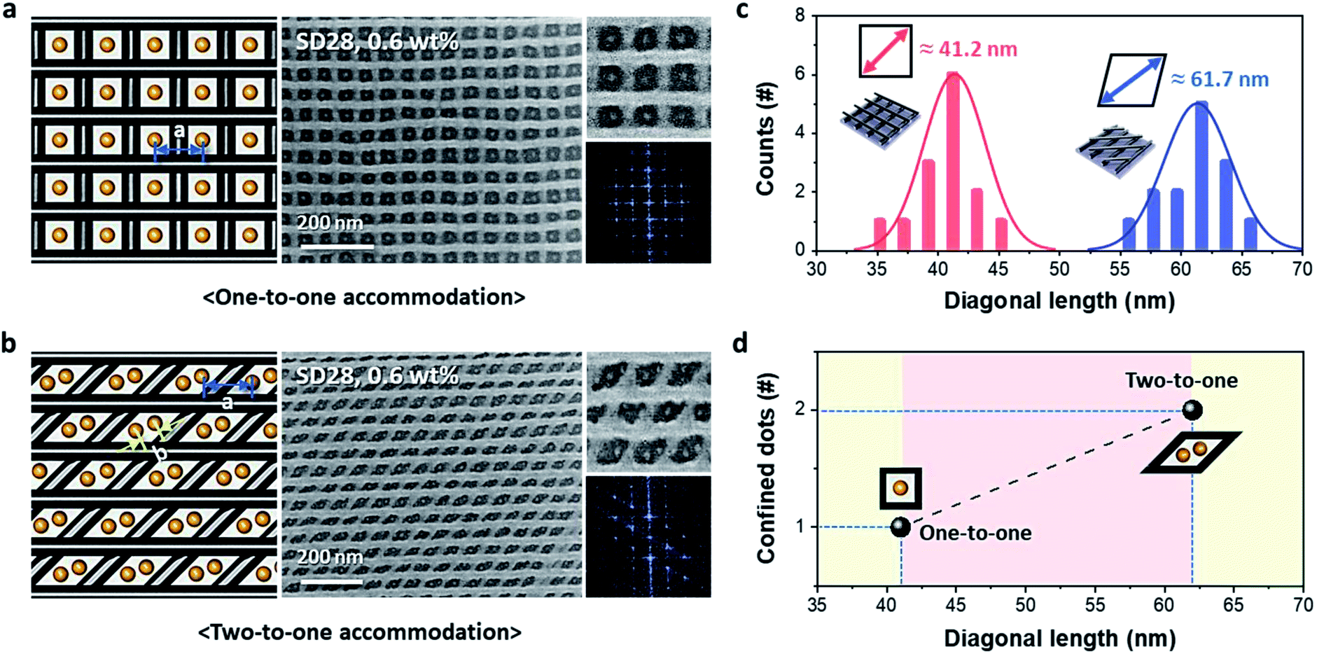 | ||
| Fig. 4 One-to-one and two-to-one accommodation of confined SiOx dots within organized cross-bar templates created by nTP. (a) One-to-one accommodation of an 8 nm SiOx dot in an Al cross-bar pattern. (b) Two-to-one accommodation of 8 nm SiOx double dots in an Al cross-bar pattern. (c) Distribution of the diagonal lengths of cross-bar Al structures. (d) Confinement range of the diagonal length for single and double SiOx nanoparticles. The inset images show FFT patterns indicating the periodicity of the templated SiOx dots by the printed cross-bar structures. | ||
Conclusions
In summary, we demonstrated a combined nanopatterning process of nTP and DSA of the BCP that effectively generates various metal/oxide hybrid 3D nanostructures, such as of line-in-mesh, dots-in-mesh, and double dots-in-mesh structures. We successfully obtained well-defined Al cross-bar structures with a sub-20 nm line width by employing a self-assembled SiOx line pattern as an nTP mold. Transfer-printed Al mesh nanostructures were used as guiding templates for the DSA of high-χ PS-b-PDMS BCPs. We clearly showed the morphological evolution from cylinders to spheres of the cylinder-forming BCP in the designated nanospaces of an Al nanomesh through the confined BCP self-assembly process by controlling the BCP film thickness. Furthermore, we demonstrated how to control the number of BCP spheres within the printed Al mesh structure with different printing angles of a repeated nTP process, showing one-to-one and two-to-one accommodation outcomes of SiOx spheres in the confined nanospaces. We expect that this multiple-nanopatterning method consisting of more than two patterning processes will be widely applicable for the useful 3D fabrication of many high-resolution devices with complex hybrid nanoarchitectures.Conflicts of interest
There are no conflicts to declare.Acknowledgements
This work was mainly supported by the National Research Foundation of Korea (NRF) grant funded by the Korea government (MSIT) (No. 2021R1A2C1004119).References
- X. Zhang, J. N. Murphy, N. L. Wu, K. D. Harris and J. M. Buriak, Macromolecules, 2011, 44, 9752–9757 CrossRef CAS.
- N. L. Wu, X. Zhang, J. N. Murphy, J. Chai, K. D. Harris and J. M. Buriak, Nano Lett., 2012, 12, 264–268 CrossRef CAS PubMed.
- Y. S. Jung, J.-B. Chang, E. Verploegen, K. K. Berggren and C. Ross, Nano Lett., 2010, 10, 1000–1005 CrossRef CAS.
- R. Ruiz, H. Kang, F. A. Detcheverry, E. Dobisz, D. S. Kercher, T. R. Albrecht, J. J. de Pablo and P. F. Nealey, Science, 2008, 321, 936–939 CrossRef CAS PubMed.
- H. Jung, W. H. Shin, T. W. Park, Y. J. Choi, Y. J. Yoon, S. H. Park, J.-H. Lim, J.-D. Kwon, J. W. Lee, S.-H. Kwon, G. H. Seong, K. H. Kim and W. I. Park, Nanoscale, 2019, 11, 8433–8441 RSC.
- J. W. Jeong, Y. H. Hur, H.-j. Kim, J. M. Kim, W. I. Park, M. J. Kim, B. J. Kim and Y. S. Jung, ACS Nano, 2013, 7, 6747–6757 CrossRef CAS PubMed.
- T. Qu, S. Guan, X. Zheng and A. Chen, Nanoscale Adv, 2020, 2, 1523–1530 RSC.
- W. I. Park, K. Kim, H. I. Jang, J. W. Jeong, J. M. Kim, J. Choi, J. H. Park and Y. S. Jung, Small, 2012, 8, 3762–3768 CrossRef CAS.
- K. W. Gotrik, A. F. Hannon, J. G. Son, B. Keller, A. Alexander-Katz and C. A. Ross, ACS Nano, 2012, 6, 8052–8059 CrossRef CAS PubMed.
- W. I. Park, J. M. Kim, J. W. Jeong and Y. S. Jung, ACS Nano, 2014, 8, 10009–10018 CrossRef CAS PubMed.
- J. G. Son, M. Son, K. J. Moon, B. H. Lee, J. M. Myoung, M. S. Strano, M. H. Ham and C. A. Ross, Adv. Mater., 2013, 25, 4723–4728 CrossRef CAS PubMed.
- Y. J. Choi, M. H. Byun, T. W. Park, S. Choi, J. Bang, H. Jung, J.-H. Cho, S.-H. Kwon, K. H. Kim and W. I. Park, ACS Appl. Nano Mater., 2019, 2, 1294–1301 CrossRef CAS.
- D. F. Sunday, X. Chen, T. R. Albrecht, D. Nowak, P. R. Delgadillo, T. Dazai, K. Miyangi, T. Maehashi, A. Yamazaki, P. F. Nealey and R. J. Kline, Chem. Mater., 2020, 32, 2399–2407 CrossRef CAS.
- J. H. Kim, H. M. Jin, G. G. Yang, K. H. Han, T. Yun, J. Y. Shin, S. J. Jeong and S. O. Kim, Adv. Funct. Mater., 2020, 30, 1902049 CrossRef CAS.
- I. Bita, J. K. Yang, Y. S. Jung, C. A. Ross, E. L. Thomas and K. K. Berggren, Science, 2008, 321, 939–943 CrossRef CAS PubMed.
- A. Rahman, P. W. Majewski, G. Doerk, C. T. Black and K. G. Yager, Nat. Commun., 2016, 7, 1–8 Search PubMed.
- A. T. KG, S. M. Nicaise, K. R. Gadelrab, A. Alexander-Katz, C. A. Ross and K. K. Berggren, Nat. Commun., 2016, 7, 1–10 Search PubMed.
- N. Demazy, C. Cummins, K. Aissou and G. Fleury, Adv. Mater. Interfaces, 2020, 7, 1901747 CrossRef CAS.
- D. S. Jung, J. Bang, T. W. Park, S. H. Lee, Y. K. Jung, M. Byun, Y.-R. Cho, K. H. Kim, G. H. Seong and W. I. Park, Nanoscale, 2019, 11, 18559–18567 RSC.
- W. I. Park, Y. K. Jung, Y. Kim, W. H. Shin, Y. J. Choi, T. W. Park, J. H. Shin, Y. H. Jeong, J. H. Cho, H. S. Shin, S.-H. Kwon, Y. S. Jung and K. H. Kim, Adv. Funct. Mater., 2019, 29, 1805795 Search PubMed.
- A. Tavakkoli KG, K. W. Gotrik, A. F. Hannon, A. Alexander-Katz, C. A. Ross and K. K. Berggren, Science, 2012, 336, 1294–1298 CrossRef CAS PubMed.
- M. S. Onses, C. Song, L. Williamson, E. Sutanto, P. M. Ferreira, A. G. Alleyne, P. F. Nealey, H. Ahn and J. A. Rogers, Nat. Nanotechnol., 2013, 8, 667 CrossRef CAS PubMed.
- A. Subramanian, G. Doerk, K. Kisslinger, H. Y. Daniel, R. B. Grubbs and C.-Y. Nam, Nanoscale, 2019, 11, 9533–9546 RSC.
- H. Y. Hsueh, Y. C. Huang, R. M. Ho, C. H. Lai, T. Makida and H. Hasegawa, Adv. Mater., 2011, 23, 3041–3046 CrossRef CAS PubMed.
- E. J. Crossland, M. Kamperman, M. Nedelcu, C. Ducati, U. Wiesner, D.-M. Smilgies, G. E. Toombes, M. A. Hillmyer, S. Ludwigs and U. Steiner, Nano Lett., 2009, 9, 2807–2812 CrossRef CAS PubMed.
- M. R. Scherer, L. Li, P. M. Cunha, O. A. Scherman and U. Steiner, Adv. Mater., 2012, 24, 1217–1221 CrossRef CAS PubMed.
- S. Park, Y. Kim, W. Lee, S.-M. Hur and D. Y. Ryu, Macromolecules, 2017, 50, 5033–5041 CrossRef CAS.
- S. Jo, H. Park, T. Jun, K. Kim, H. Jung, S. Park, B. Lee, S. Lee and D. Y. Ryu, Appl. Mater. Today, 2021, 23, 101006 CrossRef.
- J. W. Jeong, W. I. Park, L. M. Do, J. H. Park, T. H. Kim, G. Chae and Y. S. Jung, Adv. Mater., 2012, 24, 3526–3531 CrossRef CAS.
- C. Linghu, S. Zhang, C. Wang and J. Song, npj Flex. Electron., 2018, 2, 1–14 CrossRef CAS.
- H. Zhou, W. Qin, Q. Yu, H. Cheng, X. Yu and H. Wu, Nanomaterials, 2019, 9, 283 CrossRef CAS.
- S. H. Cho, K. M. Baek, H. J. Han, M. Kim, H. Park and Y. S. Jung, Adv. Funct. Mater., 2020, 30, 2000612 CrossRef CAS.
- H. Yi, M. Seong, K. Sun, I. Hwang, K. Lee, C. Cha, T. i. Kim and H. E. Jeong, Adv. Funct. Mater., 2018, 28, 1706498 CrossRef.
- J. W. Jeong, S. R. Yang, Y. H. Hur, S. W. Kim, K. M. Baek, S. Yim, H.-I. Jang, J. H. Park, S. Y. Lee, C.-O. Park and Y. S. Jung, Nat. Commun., 2014, 5, 1–12 Search PubMed.
- T. A. Pham, T. K. Nguyen, R. K. Vadivelu, T. Dinh, A. Qamar, S. Yadav, Y. Yamauchi, J. A. Rogers, N. T. Nguyen and H. P. Phan, Adv. Funct. Mater., 2020, 30, 2004655 CrossRef CAS.
- D. Chanda, K. Shigeta, S. Gupta, T. Cain, A. Carlson, A. Mihi, A. J. Baca, G. R. Bogart, P. Braun and J. A. Rogers, Nat. Nanotechnol., 2011, 6, 402–407 CrossRef CAS PubMed.
- J. Zaumseil, M. A. Meitl, J. W. Hsu, B. R. Acharya, K. W. Baldwin, Y.-L. Loo and J. A. Rogers, Nano Lett., 2003, 3, 1223–1227 CrossRef CAS.
- J. K. Hwang, S. Cho, J. M. Dang, E. B. Kwak, K. Song, J. Moon and M. M. Sung, Nat. Nanotechnol., 2010, 5, 742 CrossRef CAS.
- D. S. Wie, Y. Zhang, M. K. Kim, B. Kim, S. Park, Y.-J. Kim, P. P. Irazoqui, X. Zheng, B. Xu and C. H. Lee, Proc. Natl. Acad. Sci. U. S. A., 2018, 115, E7236–E7244 CrossRef CAS PubMed.
- T. W. Park, M. Byun, H. Jung, G. R. Lee, J. H. Park, H.-I. Jang, J. W. Lee, S. H. Kwon, S. Hong, J.-H. Lee, Y. S. Jung, K. H. Kim and W. I. Park, Sci. Adv., 2020, 6, eabb6462 CrossRef CAS PubMed.
- F. Delachat, A. Gharbi, P. Pimenta Barros, M. Argoud, C. Lapeyre, S. Bos, J. Hazart, L. Pain, C. Monget, X. Chevalier, C. Nicolet, C. Navarro, I. Cayrefourcq and R. Tiron, Proc. SPIE, 2017, 10144, 101440O CrossRef.
Footnote |
| † Electronic supplementary information (ESI) available. See DOI: 10.1039/d1na00357g |
| This journal is © The Royal Society of Chemistry 2021 |