DOI:
10.1039/D1NA00183C
(Paper)
Nanoscale Adv., 2021,
3, 4726-4738
3D graphene nanosheets from plastic waste for highly efficient HTM free perovskite solar cells
Received
11th March 2021
, Accepted 19th May 2021
First published on 20th May 2021
Abstract
Herein, we report the first time application of waste plastic derived 3D graphene nanosheets (GNs) for hole transport material (HTM) free perovskite solar cells (PSCs), where 3D GNs have been employed as an electrode dopant material in monolithic carbon electrode based mesoscopic PSCs. Waste plastics were upcycled into high-quality 3D GNs by using two-step pyrolysis processes, where, a nickel (99.99%) metal mesh was taken as the catalytic and degradation template to get an acid free route for the synthesis of 3D GNs. Raman spectroscopy, HRTEM analysis and XRD analysis show the presence of 1–2 graphene layers within the 3D GNs. Further, the optical band gap study has also been performed to analyze the applicability of 3D GNs for PSCs. The optimized device with 3D GNs shows a power conversion efficiency (PCE) of 12.40%, whereas the carbon-based control device shows a PCE of 11.04%. Further, all other device parameters such as short circuit current (Jsc), open circuit voltage (Voc) and fill factor (FF) have been improved with the addition of 3D GNs. The performance enhancement in 3D GN doped HTM free PSC solar cells is attributed to the enhancement in conductivity and reduced recombination within the device. Further, the photocurrent study shows that the 3D GN device shows better performance as compared to the reference device due to the larger diffusion current. Thus, the upcycling of waste plastics into 3D GNs and their exploitation for application in energy conversion show an effective and potential way to convert waste into energy.
1. Introduction
Recently, perovskite solar cells (PSCs) are emerging as the most efficient and cost effective solar cells, which can directly compete with traditional silicon solar cells.1,2 A perovskite solar cell consists of a perovskite structured hybrid organic–inorganic material, most commonly a lead or tin halide-based material as the light harvesting layer, which acts as an active layer within the PSC.3,4 The efficiency of PSCs has been raised to 25.5% in 2020 for single-junction architectures, which is very close to the PCE of silicon based tandem solar cells (29.1%).5 However, still research has been going on to improve all the device parameters of PSCs. Device parameters such as the PCE and stability of PSCs degrade with time, which decreases the overall performance of PSCs during long-term operation. It has been shown that this may be due to the interaction between the halide ion and Ag or Au metal based contact, which lowers the performance of PSCs.6–8 Significantly, carbon based materials have attracted immense interest as a substitute for charge collectors in PSCs due to their moisture free and heat resistant properties.9–12 In this regard, graphene has shown its capability to improve the device parameters of PSCs as an alternative to metal based charge collectors. Because of the excellent electrical conductivity and optical transparency of graphene based materials, graphene nanosheets (GNs) have been reported as efficient charge collectors in PSCs.13 Xiaojuan et al. reported the efficient charge extraction and transportation properties of graphene in planer PSCs. This group reported an improved fill factor of 82% in planar PSCs by using interface engineering with graphene and thereby showed an enhanced PCE of 20.2%.14 Nouri et al. demonstrated a reduced graphene oxide based titania layer as a hole transport layer and showed an improved fill factor of 72% with 12% PCE.15 Zang et al. reported the addition of GO as an additive material for highly efficient PSCs. Their investigations showed that addition of 1 vol% of GO over the perovskite ink increases the crystallization process and thereby showed an enhancement in the device parameters of PSCs.16 Although, 2D graphene layers had a tremendous effect on the improvement of the device parameters of PSCs, the tendency of 2D layers to get agglomerated rapidly resulted in a huge loss of the outstanding properties of graphene, hence showing poor performance in energy conversion and storage devices.17 Hence, various approaches have been identified to resolve this problem, among which the construction of 2D layers into a 3D graphene architecture showed the best promising way to tackle the problem of stacking of 2D graphene layers. The 3D architecture of graphene layers not only maintained the original properties of graphene, but this form of graphene can be easily used for application in energy conversion and storage, without the concern of the stacking problem as found in the case of 2D graphene layers. The 3D graphene architecture can be defined as the non-graphitic structure of graphene, which consists of less than 10 layers of graphene and retains almost all the excellent properties of graphene.18 Different kinds of 3D graphene architectures can be classified as (1) 3D graphene macrostructures (3D graphene monoliths) having dimensions >100 μm such as 3D graphene foams, 3D graphene aerogels, 3D graphene sponges, 3D graphene films, 3D graphene fibers, and 3D graphene milispheres,19–23 and (2) microscopic 3D graphene materials having dimensions <100 μm, which are found in powder form with nanometer or micrometer-scale 3D structures.24–26 The synthesis of these 3D graphene architectures generally consists of three main routes (1) synthesis of 3D reduced graphene oxide (rGO) from graphene oxide (GO) as a precursor material, (2) synthesis of 3D graphene nanosheets from hydrocarbons and (3) synthesis of 3D graphene from inorganic moieties such as CO, CS2, CO2etc.18 Because of the ease of synthesis methods of these new kinds of 3D graphene materials, they are extensively used in energy conversion and storage applications. 3D graphene materials are used extensively in PSCs as counter electrodes and electron-extraction interlayers i.e. these 3D graphene materials are basically used as conducting units for the faster transport of charges within interfaces.27–32 Studies showed that these 3D graphene materials not only provide faster charge transportation within interfaces, but also provide long stability against moisture and air. Presently, PSCs with the device configuration of glass/FTO/TiO2/perovskite/ZrO2/carbon showed the maximum stability up to one year33 However, because of their limited conductivity, carbon based counter electrodes showed limited PCE, but high stability. It has been reported that the limit of PCE in carbon based PSCs mainly depends on the open circuit voltage (Voc), where the determination of Voc was given as per the equationwhere EFn and EFp are the electron quasi-Fermi level and hole quasi-Fermi level. The electron quasi Fermi level depends on the interfacial contact between the ETL and perovskite layer, while the EFp depends on the interaction between the HTL and perovskite layer. In the case of HTM free PSCs, the value of EFp will be determined by the interaction between the perovskite layer and carbon layer. The predicted range of the Voc of carbon based PSCs with a HTM free configuration is about 0.8 to 1.0 V, while it is found to about 1.0 V to 1.2 V for HTM-based PSCs.34–36 Because of the higher Fermi level of −5.0 eV of carbon than the HOMO of the most of the organic HTMs such as 2,2′,7,7′-tetrakis-(N,N-di-p-methoxyphenylamine)-9,9-spirobifluorene (spiro-OMeTAD) and poly-triarylamine (PTAA) having a Fermi level of −5.2 eV and −5.25 eV, respectively, a significant reduction in Voc was observed in HTM free PSCs due to the faster charge recombination. Hence to improve the Voc and consequently, PCEs of carbon based HTM free PSCs, an efficient contact between the perovskite layer and carbon electrode must be established.37–39 In this regard, 3D graphene based materials showed their candidacy for use as counter electrode materials to enhance the device parameters of carbon based PSCs. Therefore, in the present work, we report a facile and convenient process for the improvement of the device parameters of PSCs via the doping of waste plastic derived 3D GNs. The present work not only shows an efficient way of tackling plastic waste, but also shows an excellent use of waste plastics for energy harvesting applications via upcycling into 3D GNs. A significant PCE of 12.40% was obtained for 3D GN based PSCs, and was found to be higher than those of carbon based PSCs (11.04%). Further all other device parameters such as Jsc, Voc and FF were also found to be improved with the addition of 3D GNs. Thus the present work showed a cost effective way to resolve the problem associated with waste plastics and energy crises for the sustainable conservation of “EEE” i.e. ecology, economy and energy.
2. Materials and methods
2.1 Synthesis of 3D graphene nanosheets
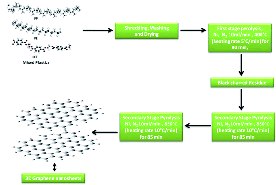
The synthesis of 3D GNs was performed as per the method reported in previous studies.40,41 However, in the present work, we modified the method by changing the degradation template for the conversion process. Nickel (99.99%) was taken as the catalytic and degradation template for the present study to get an acid free route for the synthesis of 3D GNs. Briefly, waste plastics were collected from the local market and categorized into polypropylene (PP), polyethylene (PE) and polyethylene terephthalate (PET), as these plastics contain the maximum amount of carbon in comparison to other kinds of plastics. After the categorization, the real world mix plastics (PP, PE and PET) were shredded into small flakes (average size of 10 mm × 5 mm) with the help of a shredder unit, which were later on washed with sodium hydroxide and glass washing soap solution (laboratory grade) to remove all the muddy and oily impurities from the mixed flakes of the plastics. Then the plastic flakes were dried inside a drier chamber connected with a hot air gun. Once the mixed flakes of the plastics were dried, the process of primary pyrolysis was performed inside an indigenously developed pyrolysis chamber in an inert atmosphere of N2 with a flow rate of 10 ml min−1 at the temperature of 400 °C (heating rate 10 °C min−1) for 40 min, where the feeder unit made up of stainless steel of the pyrolysis system was replaced with a nickel (99.9%) based feeder unit, which acts as a catalytic and degradation template for the upcycling of the waste plastics. Further, this step of pyrolysis removes all the petroleum products while leaving back the carbon skeleton in the form of black charred residue. The black charred residue thus obtained was then subjected to the secondary stage pyrolysis process. In our previous work, the synthesis of GNs was performed at the temperature of 750 °C. However, in the present work, we raise the temperature by another 100 °C i.e., 850 °C for the reduction of the GNs to increase the number of sp2 hybridized carbon atoms within the GNs, so that these GNs can be architectured into 3D GNs (Fig. 1), which were later on implemented as a dopant material in carbon based collectors to increase charge transportation in HTM free PSCs.
 |
| | Fig. 1 Schematic of the synthesis process of 3D GNs from plastics. | |
Generally, the formation of 3D GNs from 2D GNs can be achieved by the selective reduction of 2D GNs and the incorporation of selective catalytic systems. Depending on the nature of precursor 2D graphene materials, chemical or thermal reduction was carried out to get 3D graphene materials.42–49 Additionally, the incorporation of the metal catalyst also played a significant role in the formation of 3D GNs.50–52 Hence, the formation of 3D GNs from waste plastics also depends on the reduction process and the incorporation of selective metal catalysts. Here in the present work, we took a nickel (Ni) based bed reactor, which also acts as a catalytic template for the conversion of 2D GNs into 3D GNs. The synthesis of 2D GNs from waste plastics was performed as per our previously reported work.40,41 However, in the present work, the catalytic system was changed from a nanoclay to nickel based catalytic template to reduce the decomposition energy for the formation of 3D GNs. Further, we also raised the temperature by 100 °C to reduce 2D GNs. In the process, the well washed and shredded mixed plastics (PP, PE and PET) were allowed to undergo a primary stage pyrolysis process inside a Ni based catalytic bed reactor in the temperature range of 400 °C with a heating rate of 10 °C min−1 to get a fine skeleton of carbon residue as a building block for the growth of graphene layers, while leaving behind all kinds of value added fuels and waxy substances. After that this carbon residue was subjected to the secondary stage pyrolysis process in a secondary Ni based reactor at the temperature of 850 °C, where the process of graphenization occurred via carbon radicals which were formed from the carbon residue due to the presence of the Ni based catalyst reactor and the effect of temperature. Under the process of graphenization, the amorphous carbon atoms present within the carbon residue undergo a rearrangement and finally form a graphene like framework.53–56 Here, the Ni based bed reactor also played an important role by dissolving the carbon atoms from the decomposed plastic skeleton and thus allocated the atomic carbon atoms into an energetically favorable structure of graphene.50–52 Basically, during the synthesis of 3D GNs from plastics, the decomposition of the plastic backbone occurs as the very first step of the process, which gave birth to the active carbon building blocks for the growth of the graphene layers. Further, the thermal cracking of plastics is temperature dependent, and hence generally a higher dissociation energy is needed to break CH4-like molecules, which in turn demands higher temperature. It is estimated that generally a temperature of >1000 °C is needed to decompose CH4 molecules due to the very high activation energy (∼4.85 eV) of the C–H bond in methane.57 Hence, the use of a metal catalyst is always preferred to reduce the decomposition temperature. Especially, a Ni based catalyst showed a significant effect on the temperature reduction for the decomposition of CH4. The thermal cracking of CH4 over the Ni based catalyst is endothermic in nature;58
| | | CH4 → C + 2H2; ΔH (298 K) = 74.52 kJ mol−1 | (2) |
The Gibbs energy ΔG° for this reaction with respect to temperature as per the thermodynamic calculations is given as
| | | ΔG° (J mol−1) = 89658.88 – 102.27 × T − 0.00428 × T2 − 2499358.99/T | (3) |
So, fromeqn (2), it is found that above temperature 544 °C, ΔG° is found to be below zero and thus cracking of CH4 on the Ni catalyst will be displaced towards the growth of carbon and hydrogen. The carbon atoms thus generated tend to undergo graphenization, while hydrogen atoms have combined to form H2 gas.58–60 Thus, Ni based catalysts were selectively chosen for the present study to form 3D GNs. The final product after the secondary stage pyrolysis was then characterized to confirm the applicability of the thus synthesized 3D GNs for application in PSCs.
2.2 Characterization
The 3D GNs obtained after the secondary stage pyrolysis process were characterized by spectroscopic and imaging techniques. Raman spectroscopy was performed by using an AIRIX, STR 500 confocal micro Raman spectrometer with an excitation beam length of 532 nm in order to confirm the synthesis of 3D GNs. The presence of various functionalities was confirmed by using FT-IR spectroscopy with an FT-IR spectrometer, PerkinElmer, Lambda-2. UV-visible spectroscopy was performed to get the absorption and optical band gap properties of the 3D GNs, Field emission scanning electron microscopy (FESEM) was performed by using a NOVA FESEM 900. High resolution transmission electron microscopy (HRTEM) was performed by using a JEOL, JEM 2100 microscope to get the internal morphology. X-ray diffraction spectroscopy was performed with a Rigaku Miniflex-II by using Cu-Kα radiation of wavelength k = 1.5418 Å. Thermal gravimetric spectroscopy was performed by using a TGA 4000, PerkinElmer to get the thermal behaviour of 3D GNs. The electronic band gap (Eg) of the 3D GNs was evaluated by using cyclic-voltammetry.
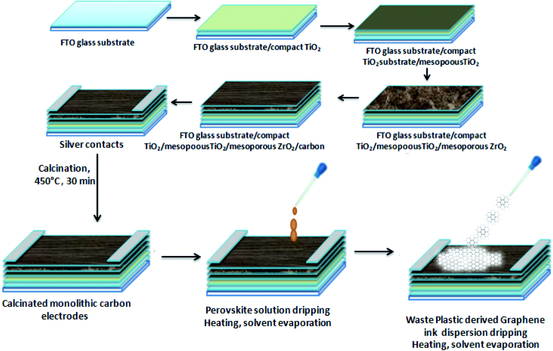
2.3 Device fabrication
The fabrication of HTM free PSCs was done on carbon monolithic electrodes (Solaronix) with an active carbon area of 12 × 15.5 mm2. Carbon monolithic electrodes were heated at 450 °C inside a vacuum oven for 30 min and cooled down subsequently to attain the room temperature. After that perovskite ink was prepared by taking a 1![[thin space (1/6-em)]](https://www.rsc.org/images/entities/char_2009.gif) :1 molar ratio of PbI2 and methyl ammonium iodide (MAI) in 1 ml of dimethyl formamide (DMF) inside a nitrogen glove box. Two PSCs were fabricated in two configurations. One of the devices (D1) was fabricated by depositing the perovskite ink via the drop casting method over carbon monolithic electrodes. Thereafter, it was annealed for 10 min at 70 °C, while the other device (D2) was fabricated by first depositing the perovskite ink via the drop casting method and another drop of the dispersion of waste plastic derived 3D GNs in chlorobenzene (10 mg in 20 ml) was subsequently added. The device thus obtained is left for 1 min in order to achieve uniform spreading of the ink and dispersion of the 3D GNs and annealed for 10 min at 70 °C in order to get complete 3D GN based perovskite solar cells.
:1 molar ratio of PbI2 and methyl ammonium iodide (MAI) in 1 ml of dimethyl formamide (DMF) inside a nitrogen glove box. Two PSCs were fabricated in two configurations. One of the devices (D1) was fabricated by depositing the perovskite ink via the drop casting method over carbon monolithic electrodes. Thereafter, it was annealed for 10 min at 70 °C, while the other device (D2) was fabricated by first depositing the perovskite ink via the drop casting method and another drop of the dispersion of waste plastic derived 3D GNs in chlorobenzene (10 mg in 20 ml) was subsequently added. The device thus obtained is left for 1 min in order to achieve uniform spreading of the ink and dispersion of the 3D GNs and annealed for 10 min at 70 °C in order to get complete 3D GN based perovskite solar cells.
2.4 Device characterization
The J–V measurements of the devices were performed using a Keithley 2420 source measure unit system. A solar simulator AM 1.5G (class AAA, Photo Emission Tech) was used for the illumination purpose.
3. Results and discussion
The 3D GNs thus obtained from waste plastics were characterized in order to understand the different properties of the 3D GNs. The Raman spectrum of the thus synthesized 3D GNs showed two prominent peaks at 1345.77 cm−1 and 1598.38 cm−1 corresponding to the D and G bands of the 3D GNs (Fig. 2(a)). The D band showed defects present within the 3D GNs and the presence of the sp3 hybridized carbon atom within the 3D GNs. These sp3 hybridized carbon atoms within the 3D GNs rose during the synthesis of the 3D GNs. However, the intensity of the D band in the present case was found to be less intense in comparison to our previously reported 2D GNs at lower temperature.40 The G band at 1591 cm−1 showed a precisely sharp peak with the presence of the sp2 hybridized carbon atoms within the 3D GNs. Further, this band also showed the 1st order scattering of these sp2 hybridized carbon atoms due to the presence of E2g vibration mode. The intensity of the D band showed the information of the domains of sp2 carbons within the 3D GNs, while the average sizes of the domains of sp2 carbons were depicted by the ID/IG ratio.61–65 The ID/IG ratio for the 3D GNs was found to be 0.84, thereby showing that there are more domains of sp2 carbons within the 3D GNs. Additionally, another bands at 2690.99 cm−1 and 2923.05 cm−1 depicted the presence of 2D and D + G bands due to the process of double resonance. The presence of the 2D band demonstrated the presence of few layer graphene sheets within 3D GNs, which is again confirmed by the I2D/IG ratio, which showed a value of 0.18, while the presence of the D + G band with high intensity showed less disorderness within the 3D GNs. Further, XRD analysis of the 3D GNs was also performed in order to evaluate the number of graphene layers present within each stack of the 3D GNs. Fig. 2(b) shows the XRD spectrum of the 3D GNs, which showed broad diffraction peaks at 2θ = 24.87° and 43.91°, corresponding to the characteristic peak and graphitic peaks of the reduced form of GNs.66
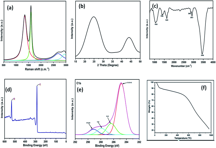 |
| | Fig. 2 (a) Raman spectra of 3D GNs; (b) XRD graph of 3D GNs; (c) FT-IR spectra of 3D GNs; (d) wide scan XPS of 3D GNs; (e) high resolution XPS of 3D GNs; (f) TGA graph of 3D GNs. | |
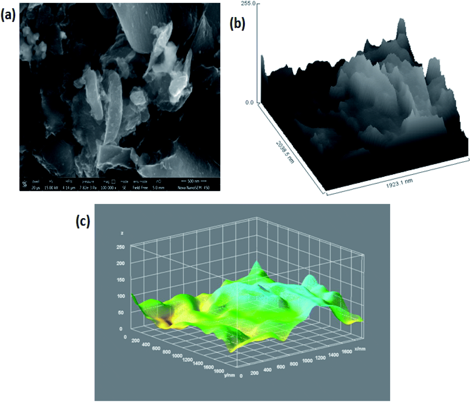
Again, in order to perform the thickness measurement and measure the number of layers present within the 3D GNs, Scherrer's equation and Bragg's equation were applied, as reported previously.67–69 Accordingly, the number of layers present within each stack of 3D GNs can be calculated by dividing the crystal size (C) with the interlayer distance (d) between the graphene layers followed by the addition of 0.1 nm corresponding to the thickness of one graphene sheet. Here, in the present case, the calculated crystal size (C) of the 3D GNs was found to be 10.33 Å corresponding to the diffraction peak of 2θ = 24.87°, while the interlayer distance (d) between the graphene layers was found to be 5.539 Å. Thus, as per the crystal size (C) and interlayer distance calculated (d) from the XRD data, about 1–2 graphene layers were found within each stack of 3D GNs. Further, in order to analyze the type of functionalities present within the 3D GNs, FT-IR analysis was carried out. Fig. 2(c) shows the FT-IR spectrum of the 3D GNs, and shows the presence of various oxygen containing functionalities within the 3D GNs. The FT-IR spectra of 3D GNs showed a strong and broad peak at 3440 cm−1, weak and sharp peak at 2921 cm−1, weak peak at 2862 cm−1, medium and sharp peak 1629 cm−1, medium and broad peak at 1386 cm−1, and medium and broad peak at 1063 cm−1 corresponding to –OH stretching, –CH stretching, –C![[double bond, length as m-dash]](https://www.rsc.org/images/entities/char_e001.gif) C– stretching, –CH bending and –C–O stretching, respectively. Again to correlate the presence of these oxygen functionalities within the 3D GNs, X-ray photoelectron spectroscopy (XPS) was also performed in order to analyze the properties of the 3D GNs. The wide scan XPS spectra of 3D GNs showed the presence of only carbon and oxygen within the 3D GNs as shown in Fig. 1(d), while the high resolution XPS spectra showed a sharp peak at 284.7 eV corresponding to the CC/C–C and the peaks at 286.4 eV, 287.9 eV, and 289.3 eV correspond to C–O in hydroxyl and epoxy groups, and O–CO in carboxyl groups, respectively, as shown in Fig. 1(e).70–73 Further, thermal gravimetric analysis (TGA) was performed in order to understand the skeleton and purity of the 3D GNs. The TGA curve of reduced graphene nanosheets showed three stage weight loss reduction in the ranges of 30 °C to 100 °C, 100 °C to 550 °C and from 550 °C to 950 °C. The first stage weight loss occurred due to the presence of the moisture content present within the 3D GNs, while the second and third stage reduction was found to be mainly due to the elimination of oxygen functionalities and degradation of the carbon backbone (Fig. 2(e)). Again, the surface morphology of these 3D GNs was also investigated by FESEM analysis. Fig. 3(a) shows the FESEM images of the 3D GNs, which clearly show the clusters of graphene layers with the occurrence of wrinkles at the surfaces. Further, Fig. 3(b) shows the Hill plot profile of the 3D GNs, which shows the uneven hills of the graphene layers with varying sheet areas within the 3D GNs. The Hill plot also showed curly edges with sharp spikes within the graphene layers of the 3D GNs, which developed defects within the 3D GNs and thereby showed metallic nature within these 3D GNs, as reported in our previous study.40
C– stretching, –CH bending and –C–O stretching, respectively. Again to correlate the presence of these oxygen functionalities within the 3D GNs, X-ray photoelectron spectroscopy (XPS) was also performed in order to analyze the properties of the 3D GNs. The wide scan XPS spectra of 3D GNs showed the presence of only carbon and oxygen within the 3D GNs as shown in Fig. 1(d), while the high resolution XPS spectra showed a sharp peak at 284.7 eV corresponding to the CC/C–C and the peaks at 286.4 eV, 287.9 eV, and 289.3 eV correspond to C–O in hydroxyl and epoxy groups, and O–CO in carboxyl groups, respectively, as shown in Fig. 1(e).70–73 Further, thermal gravimetric analysis (TGA) was performed in order to understand the skeleton and purity of the 3D GNs. The TGA curve of reduced graphene nanosheets showed three stage weight loss reduction in the ranges of 30 °C to 100 °C, 100 °C to 550 °C and from 550 °C to 950 °C. The first stage weight loss occurred due to the presence of the moisture content present within the 3D GNs, while the second and third stage reduction was found to be mainly due to the elimination of oxygen functionalities and degradation of the carbon backbone (Fig. 2(e)). Again, the surface morphology of these 3D GNs was also investigated by FESEM analysis. Fig. 3(a) shows the FESEM images of the 3D GNs, which clearly show the clusters of graphene layers with the occurrence of wrinkles at the surfaces. Further, Fig. 3(b) shows the Hill plot profile of the 3D GNs, which shows the uneven hills of the graphene layers with varying sheet areas within the 3D GNs. The Hill plot also showed curly edges with sharp spikes within the graphene layers of the 3D GNs, which developed defects within the 3D GNs and thereby showed metallic nature within these 3D GNs, as reported in our previous study.40
 |
| | Fig. 3 (a) FESEM image of 3D GNs at a magnification of 500 nm; (b) hill stack plot of 3D GNs; (c) 3D surface morphology of the 3D GNs. | |
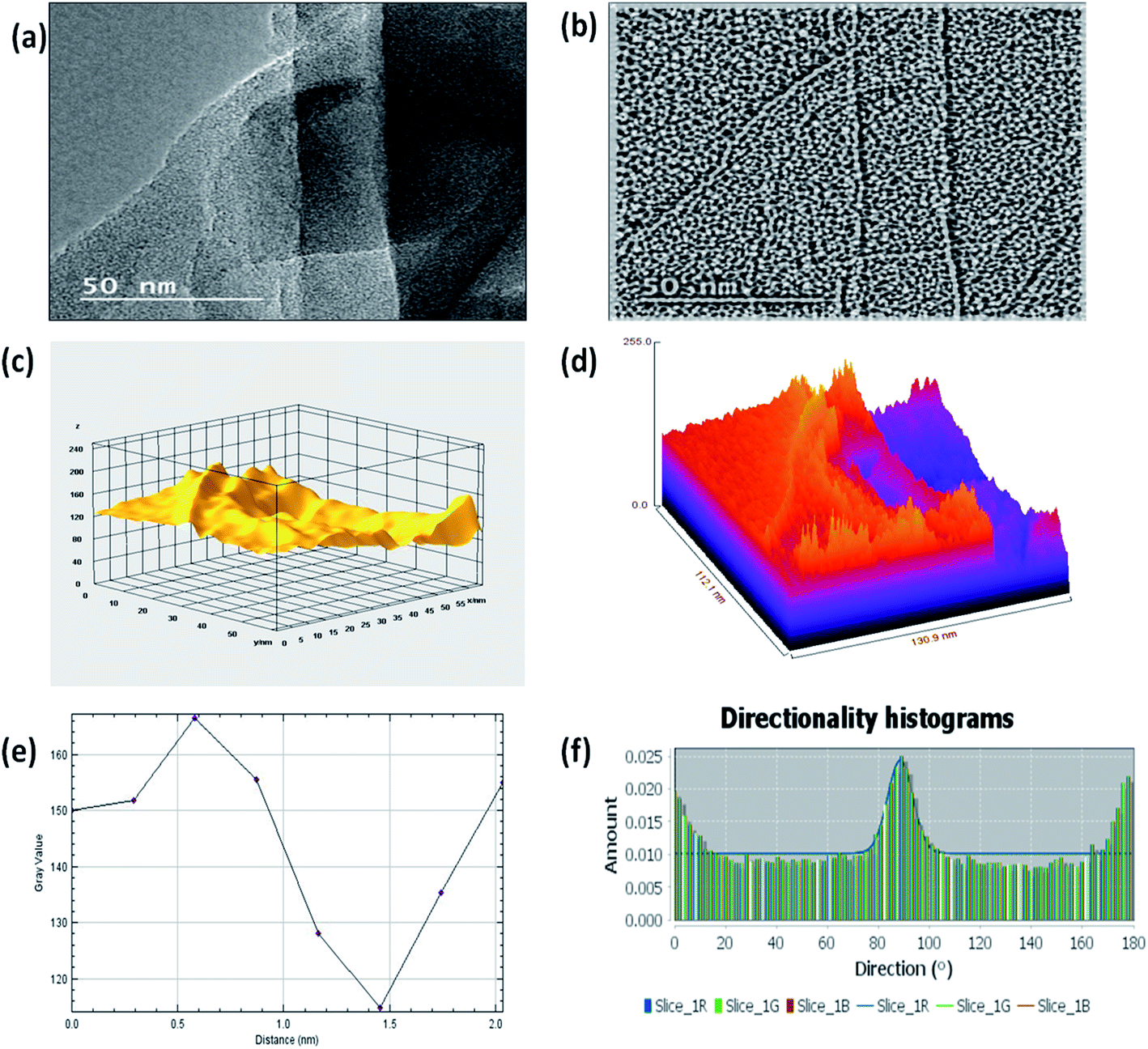
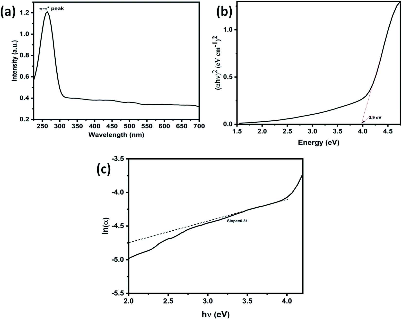
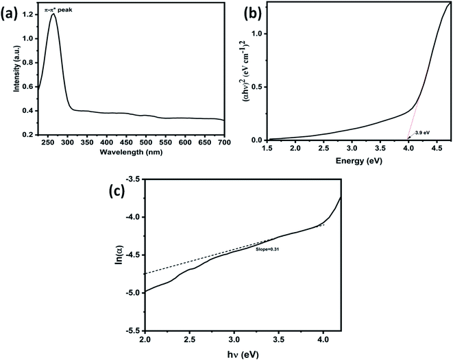
Further, Fig. 3(c) shows the 3D surface morphology of the 3D GNs in a white spectrum form to show the continuity within the 3D GNs. The 3D surface morphology showed the wrinkled morphology of the GNs along the x, y and z axis, which showed the 3D nature of the GNs. Further, the surfaces of the 3D GNs, where the layers are stacked in a regular morphology, are shown with blue contrast, while the places where the layers show random morphology are shown with higher wavelength colours i.e. yellow and green, which depict the uneven distribution of the graphene layers within the 3D GNs. However, it is often difficult to find out the exact number of layers by analyzing the FESEM images, and hence HRTEM analysis was carried out in order to get the average number of graphene layers present within each stack of 3D GNs. Fig. 4(a) shows the HRTEM images of the 3D GNs at the magnification of 50 nm. The HRTEM image of the 3D GNs shows the presence of corrugated edges, along with different kinds of grain boundaries, thereby showing polycrystalline properties within the 3D GNs, which were also confirmed from the shape index image of the 3D GNs (Fig. 4(b)). Further, the 3D surface morphology from the HRTEM analysis showed that each GN perfectly overlapped with each other and thereby maintained the continuity to form the 3D network of the GNs (Fig. 4(c)), which can also be seen from the Hill stack plot of the 3D GNs, where each crest of the GNs perfectly linked with another crest of GNs having unlike dimensions with respect to their adjacent GNs (Fig. 4(d)). Again the thickness measurement of the GNs in 3D GNs was performed, which showed the presence of 1–2 nm thick sheets of GNs (Fig. 4(e)). Further the directional properties of these GNs also confirmed the 3D alignment of GNs as seen from the directionality histograms (Fig. 4(f)). The directionally histogram showed that most of the GNs aligned vertically to make a 3D network of the GNs. After analyzing the various properties of the thus synthesized 3D GNs, the viability of the thus obtained 3D GNs was investigated for application in PSCs. Thus, UV-Visible spectroscopy was performed to analyze the band gap properties of the 3D GNs (Fig. 5(a)). The UV-Vis spectrum of the thus synthesized 3D GNs showed a peak maximum at 263 nm corresponding to the π–π* transitions of CC bonds of the extended aromatic system of the 3D GNs. Based on the absorption maximum of the 3D GNs, the optical band of the 3D GNs was obtained by plotting the Tauc plot according to the following relation
where the absorption coefficient (
α) is directly related to the incident photons and
Eopt is known as the optical band gap of the material. The calculated
Eopt of the 3D GNs was found to be 3.9 eV, which is found to be similar to previously reported optical band gaps for graphene-based materials,
74 where these graphene based materials can be employed as candidates for electrode materials for various photovoltaic devices (
Fig. 5(b)). Further, Urbach energy (
Eu) was also evaluated to estimate the band gap (
Eg) between the HOMO/LUMO of the 3D GNs by using the following relation
where the urbach tail (
Eu) is related to the absorption coefficient as
α =
α0exp(
hυ/
Eu) in the low energy tail of the absorption spectrum.
75Fig. 5(c) shows the ln
α–
hυ plot of 3D GNs, accordingly, the
Eu from this plot can be calculated as the reciprocal of the inclined slope of the linear fitting, which is found to be 3.3 eV. Thus, from
eqn (5), the estimated
Eg of the 3D GNs was found to be 0.6 eV, which is found to be very close to the previous literature reports of graphene based materials.
76
 |
| | Fig. 4 (a) HRTEM image of 3D GNs, (b) shape index image of 3D GNs from the HRTEM image (c) 3D surface morphology from HRTEM analysis (d) Hill stack plot of 3D GNs from HRTEM analysis; (e) plot profile diagram showing the average thickness of GNs in 3D GNs; (f) directionality histogram of the 3D GNs showing the directional alignment of the GNs within the 3D GNs. | |
 |
| | Fig. 5 (a) UV-visible spectra of waste plastic derived 3D GNs, (b) (αhυ)2vs. energy plot of waste plastic derived 3D GNs, and (c) lnα vs. hυ plot of waste plastic derived 3D GNs. | |
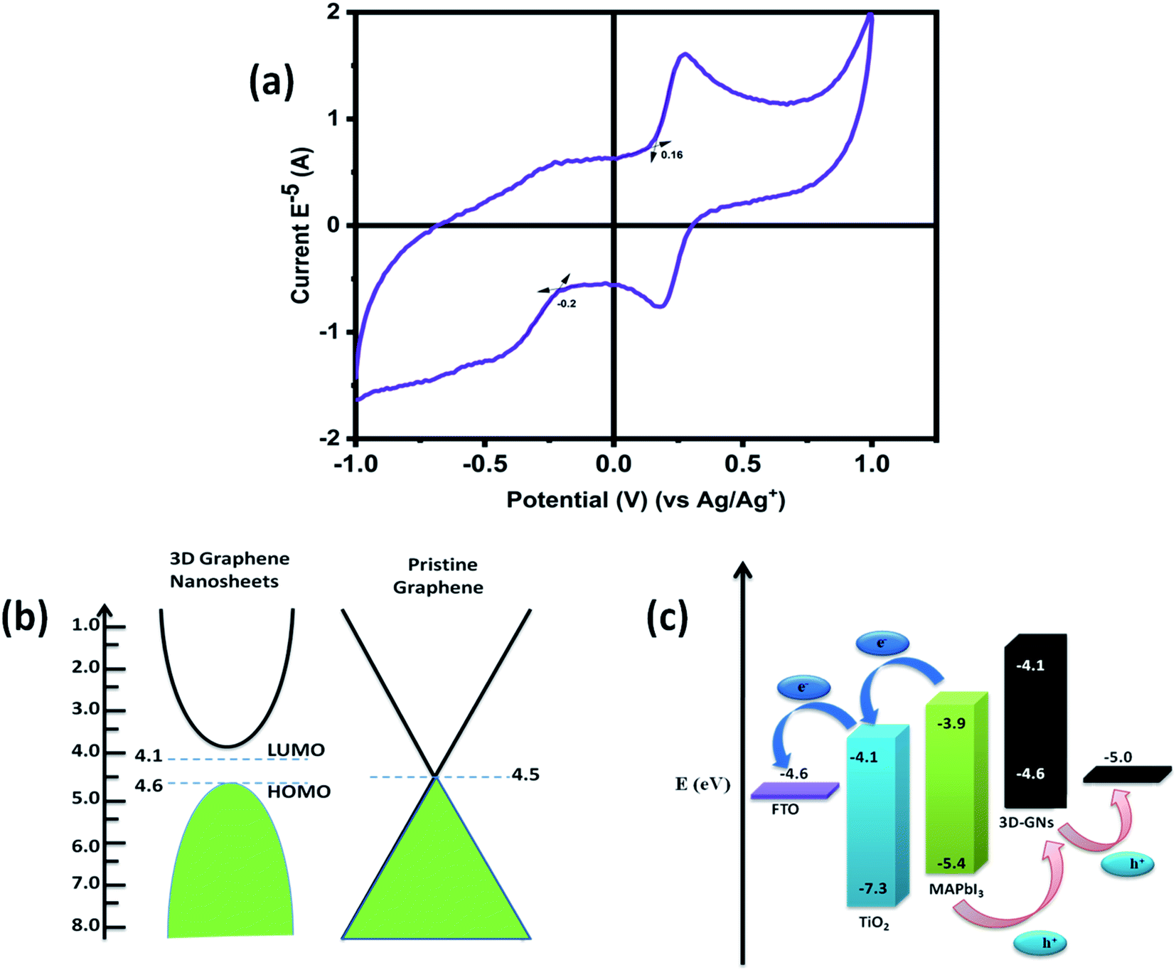
Further, cyclic voltammetry analysis was also performed in order to evaluate the valence band maximum (VBM) level (HOMO) and conduction band maximum (CBM) level (LUMO) of the 3D GNs (Fig. 5(a)). The calculation of the VBM and CBM of the 3D GNs was done by analyzing the onset oxidation potential (Eoxi) and onset reduction potential (Ered) by using eqn (4)–(6), as shown below.77
| | | EVBM = [Eoxi − E1/2(ferrocene) + 4.8] eV | (6) |
| | | ECBM = [Ered − E1/2(ferrocene) + 4.8] eV | (7) |
In the above equations, the value of E1/2 (ferrocene) was obtained as 0.41 V. Fig. 5(a) shows the cyclic voltammogram of the thus synthesized 3D GNs. The calculated VBM and CBM levels for the 3D GNs from eqn (6) and (7) were found to be −4.6 eV and −4.1 eV, respectively. Further these values of VBM and CBM of 3D GNs were also very closer to each other and approach nearer to the Fermi level of the pristine graphene (Fig. 5(b)). Thus, from eqn (8), the band gap (Eg) of the 3D GNs was found to be 0.5 eV, which showed a very close proximity to the evaluated band gap by UV-visible analysis. The obtained value of Eg for the 3D GNs showed that these 3D GNs are perfectly suited for application as electrodes in energy harvesting.
Hence, in order to identify the real time utility of the 3D GNs, we have fabricated carbon-based PSCs and doped them with these 3D GNs to enhance the device parameters of PSCs, as graphene is popularly known for faster charge transportation and thereby helps to improve the device parameters of the photovoltaic devices. Fig. 6(c) shows the energy level diagram of the 3D GN doped carbon-PSCs, which showed that a favourable HOMO level of the 3D GNs can easily facilitate smoother charge transportation of the holes, thereby doping these 3D GNs can significantly improve the device parameters of carbon-PSCs. So, one of the PSC devices (D1) was fabricated on the printed monolithic carbon electrode having the configuration of Glass/FTO/TiO2/ZrO2/conductive carbon by depositing the perovskite layer via the drop casting method and subsequently annealed at 70 °C for 10 min, while in the PSC device (D2), fabrication on the same monolithic carbon electrode was done by drop casting of the same perovskite ink followed by doping of the dispersion of 3D GNs in chlorobenzene and annealing at 70 °C for 10 min (Fig. 7). In both the devices, the perovskite ink was absorbed by the subsequent layers of the printed monolithic carbon electrodes through the channelized porous holes of the carbon layer.
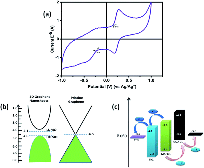 |
| | Fig. 6 (a) Cyclic voltammograms of waste plastic derived 3D GNs, (b) HOMO–LUMO positions of waste plastic derived 3D GNs and pristine graphene, and (c) energy level diagram of waste plastic derived 3D GN based carbon-PSCs. | |
 |
| | Fig. 7 Schematic of the device fabrication of the HTM free PSC with 3D GNs. | |
However, in device D2, after absorbing the perovskite ink, a dense dispersion of 3D GNs was added subsequently in order to dope the upper layer of the electrode with 3D GNs (Fig. 8(a)). Because of the high surface area of 3D GNs, the particles of the 3D GNs do not cross the microchannels of the porous carbon layer and thereby spread uniformly on the surface of the carbon layer. Additionally, the dispersion of 3D GNs in chlorobenzene acts as a dual performer to improve the device performance, as the chlorobenzene also helps in the adduct formation during the fabrication of PSCs.78 Once the fabrication of both the devices was completed, J–V characteristics of the devices were measured by using a Keithley 4200 semiconductor and solar simulator AM 1.5G (class AAA, Photo Emission Tech.) for the illumination purpose. Fig. 8(b) shows the J–V characteristics of PSC devices D1 (reference) and D2 (carbon + 3D GNs). The improvement in various device parameters has been observed with the 3D GN-doped device (D2) as compared to the reference device (D1) as shown in Table 1.
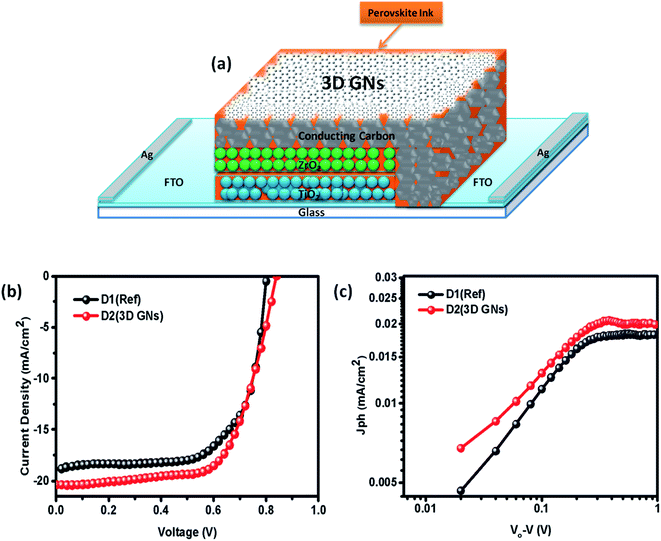 |
| | Fig. 8 (a) Device geometry of the 3D GN-doped PSC (b) J–V characteristics of PSC devices D1 (reference) and D2 (carbon + 3D GNs), and (c) photocurrents for PSC devices D1 (reference) and D2 (carbon + 3D GNs). | |
Table 1 Different device parameters for both the devices D1 and D2
| Device |
J
sc (mA cm−2) |
V
oc (V) |
FF (%) |
η (%) |
| D1 |
18.93 |
0. 82 |
64.00 |
11.04 |
| D2 |
20.34 |
0.84 |
65.31 |
12.40 |
The recorded short circuit current (Jsc) for D1 is found to be 18.93 mA cm−2, whereas the 3D GN-doped device showed an enhanced Jsc up to 20.34 mA cm−2. An improvement in open circuit voltage (Voc) and fill factor (FF) has also been observed. The Voc has been increased by 0.02 V and FF by 1.31%. As seen from the energy level diagram, the VBM of 3D GNs matched well with the VBM of PSCs, which allowed smoother and effective transportation of holes from the perovskite layer towards the 3D GNs/carbon electrode. Thus, the introduction of 3D GNs within the carbon electrode effectively retards the process of recombination, which can be seen from the enhanced value of Voc (Fig. 6(c)). Hence, the overall PCE has been increased from 11.04% to 12.40%. The performance enhancement in the 3D GN-doped solar cell is attributed to the enhancement in conductivity and reduced recombination within the device. Further, the photocurrent (Jph) has been estimated to understand the enhancement in device performance by subtracting the dark current from the light current (Jph = JL − JD) and plotted against the effective applied bias Veff (V0 − V) on the logarithmic scale for both devices D1 and D2 (Fig. 8(c)). The effective bias has been evaluated by the subtraction of applied bias voltage from the compensation voltage (V0) where the compensation voltage is the voltage at which the light current is equal to the dark current, i.e., JL = JD. The effective applied bias implies the strength of the overall internal electric field of devices.79 Generally, such a plot has two prominent sections i.e. diffusion and drift corresponding to the low and high electric field. For D1 the effective bias (V0 − V < 0.23 V) indicates that a small electric field exists within the device for which the photocurrent increases almost linearly with the effective bias and it tends to saturate after 0.23 V which is governed by the external field and temperature dependent e–h pairs. For D2 the inflection point from linear to saturation occurs at 0.27 V which is slightly higher than that of the reference device that refers to the larger diffusion current within the 3D GN device leading to better performance as compared to the reference device.
Thus, the overall study showed that the synthesis of 3D GNs not only significantly reduces the carbon footprint and environmental pollution from waste plastics, but it also showed a potential solution by the process of upcycling to tackle the problem of economy and energy crises in a very cost effective manner.
4. Conclusion
In conclusion, we have successfully demonstrated the utility of the process of upcycling for plastic waste management by converting them into high quality 3D GNs for application in PSCs. Raman spectroscopy, HRTEM analysis and XRD analysis showed the presence of 1–2 layers of GNs within 3D GNs. The 3D GNs thus obtained are found to be conductive, and are perfectly suited as an electrode material for PSCs. The band gap obtained for 3D GNs showed that they could be perfectly used as an electrode material for photovoltaic applications. A significant PCE of 12.40% was obtained for 3D GN-based PSCs, which is found to be higher than those of carbon based PSCs having a PCE of 11.04%. Further, all other device parameters such as Jsc, Voc and FF were also found to be improved with the addition of 3D GNs. The performance enhancement in the 3D GN-doped solar cell is attributed to the enhancement in conductivity and reduced recombination within the device. Further, the photocurrent study showed that the 3D GN device leads to better performance as compared to the reference device due to the larger diffusion current. Thus, the upcycling of waste plastics into reduced graphene nanosheets and their exploitation for application in energy conversion showed an effective and potential way of tackling the problem of plastic waste in the environment.
Data availability
The data that support the plots within this paper and other findings of this study are available from the corresponding author upon reasonable request.
Author contributions
Sandeep Pandey: conceptualization, methodology, investigation, software, writing-original draft. Amit Kumar: methodology, device fabrication. Manoj Karakoti: methodology Kuldeep K. Garg: formal analysis: Aniket Rana: software, writing and review. Gaurav Tatrari: formal analysis, Bhashkar Singh Bohra: analysis and writing, Pankaj Yadav: formal analysis and review. Rajiv K. Singh: formal analysis & review, Nanda Gopal Sahoo: co-ordinated overall work, review & editing.
Conflicts of interest
We declare that we have no conflict of interest.
Acknowledgements
The authors acknowledge the financial support from the DST INSPIRE division (IF150750) and DST-FIST New Delhi, India, the National Mission on Himalayan Studies, GBPHIED, Kosi-Katarmal, Almora, Uttarakhand, India, and the Council of Scientific and Industrial Research, New Delhi, India.
References
- N. G. Park, Mater. Today Commun., 2015, 18(2), 65–72, DOI:10.1016/j.mattod.2014.07.007.
- M. I. H. Ansari, A. Qurashi and M. K. Nazeeruddin, J. Photochem. Photobiol., C, 2018, 35, 1–24, DOI:10.1016/j.otochemrev.2017.11.002.
- T. Baikie, Y. Fang, J. M. Kadro, M. Schreyer, F. Wei, S. G. Mhaisalkar, M. Graetzel and T. J. White, J. Mater. Chem. A, 2013, 1(18), 5628–5641, 10.1039/C3TA10518K.
- N. J. Jeon, J. H. Noh, Y. C. Kim, W. S. Yang, S. Ryu and S. I. Seok, Nat. Mater., 2014, 13(9), 897–903, DOI:10.1038/nmat4014.
- https://www.nrel.gov/pv/assets/pdfs/best-research-cell-efficiencies.20200104.pdf.
- Y. Han, S. Meyer, Y. Dkhissi, K. Weber, J. M. Pringle, U. Bach, L. Spiccia and Y. B. Cheng, J. Mater. Chem. A, 2015, 3(15), 8139–8147, 10.1039/C5TA00358J.
- K. Domanski, J. P. Correa-Baena, N. Mine, M. K. Nazeeruddin, A. Abate, M. Saliba, W. Tress, A. Hagfeldt and M. Grätzel, ACS Nano, 2016, 10(6), 6306–6314, DOI:10.1021/acsnano.6b02613.
- A. Guerrero, J. You, C. Aranda, Y. S. Kang, G. Garcia-Belmonte, H. Zhou, J. Bisquert and Y. Yang, ACS Nano, 2016, 10(6), 218–224, DOI:10.1021/acsnano.5b03687.
- A. Mei, X. Li, L. Liu, Z. Ku, T. Liu, Y. Rong, M. Xu, M. Hu, J. Chen, Y. Yang, M. Grätzel and H. Han, Science, 2014, 345(6194), 295–298, DOI:10.1126/science.1254763.
- P. You, Z. Liu, Q. Tai, S. Liu and F. Yan, Adv. Mater., 2015, 27(24), 3632–3638, DOI:10.1002/adma.201501145.
- X. Meng, J. Zhou, J. Hou, X. Tao, S. H. Cheung, S. K. So and S. Yang, Adv. Mater., 2018, 30(21), 1706975, DOI:10.1002/adma.201706975.
- A. Verma, D. Martineau, S. Abdolhosseinzadeh, J. Heier and F. Nüesch, Mater. Adv., 2020, 1(2), 153–160, 10.1039/D0MA00077A.
- C. Zhang, S. Wang, H. Zhang, Y. Feng, W. Tian, Y. Yan, J. Bian, Y. Wang, S. Jin, S. M. Zakeeruddin, M. Grätzel and Y. Shi, Energy Environ. Sci., 2019, 12(12), 3585–3594, 10.1039/C9EE02391G.
- X. Zhao, L. Tao, H. Li, W. Huang, P. Sun, J. Liu, S. Liu, Q. Sun, Z. Cui, L. Sun, Y. Shen, Y. Yang and M. Wang, Nano Lett., 2018, 18(4), 2442–2449, DOI:10.1021/acs.nanolett.8b00025.
- E. Nouri, M. R. Mohammadi, Z. X. Xu, V. Dracopoulos and P. Lianos, Phys. Chem. Chem. Phys., 2018, 20(4), 2388–2395, 10.1039/C7CP04538G.
- X. Zhang, G. Ji, D. Xiong, Z. Su, B. Zhao, K. Shen, Y. Yang and X. Gao, RSC Adv., 2018, 8(2), 987–993, DOI:10.1021/nl102661q.
- C. Liu, Z. Yu, D. Neff, A. Zhamu and B. Z. Jang, Nano Lett., 2010, 10(12), 4863–4868, DOI:10.1021/nl102661q.
- Z. Sun, S. Fang and Y. H. Hu, Chem. Sci., 2020, 120(18), 10336–10453, DOI:10.1021/acs.chemrev.0c00083.
- Y. Zhang, Y. Huang, T. Zhang, H. Chang, P. Xiao, H. Chen, Z. Huang and Y. Chen, Adv. Mater., 2010, 27(12), 2049–2053, DOI:10.1002/adma.201405788.
- Y. Zhao, J. Liu, Y. Hu, H. Cheng, C. Hu, C. Jiang, L. Jiang, A. Cao and L. Qu, Adv. Mater., 2013, 25(4), 591–595, DOI:10.1002/adma.201203578.
- L. Kou, Z. Liu, T. Huang, B. Zheng, Z. Tian, Z. Deng and C. Gao, Nanoscale, 2015, 7(9), 4080–4087, DOI:10.1021/nn3021772.
- Z. Xu, Y. Zhang, P. Li and C. Gao, ACS Nano, 2012, 6(8), 7103–7113, DOI:10.1021/nn3021772.
- C. Yang, Y. Xu, C. Zhang, Z. Sun, C. Chen, X. Li, S. Jiang and B. Man, Nanoscale Res. Lett., 2014, 9(1), 1–6, DOI:10.1186/1556-276X-9-394.
- H. Wang, K. Sun, F. Tao, D. J. Stacchiola and Y. H. Hu, Angew. Chem., Int. Ed., 2013, 52(35), 9210–9214, DOI:10.1002/anie.201303497.
- W. Wei, K. Sun and Y. H. Hu, J. Mater. Chem. A, 2014, 2(40), 16842–16846, DOI:10.1002/anie.201303497.
- L. Chang, W. Wei, K. Sun and Y. H. Hu, J. Mater. Chem. A, 2015, 3(9), 10183–10187, 10.1039/C5TA01055A.
- P. You, Z. Liu, Q. Tai, S. Liu and F. Yan, Adv. Mater., 2015, 27(24), 3632–3638, DOI:10.1002/adma.201501145.
- Y. Wang, Y. Jin, C. Zhao, E. Pan and M. Jia, J. Colloid Interface Sci., 2018, 532, 352–362, DOI:10.1016/j.jcis.2018.08.011.
- P. Yang, Z. J. Hu, X. C. Zhao, D. Chen, H. Lin, X. C. Lai and L. J. Yang, Chemistryselect, 2017, 2(29), 9433–9437, DOI:10.1002/slct.201701479.
- J. T. W. Wang, J. M. Ball, E. M. Barea, A. Abate, J. A. AlexanderWebber, J. Huang, M. Saliba, L. Mora-Sero, J. Bisquert, H. J. Snaith and R. J. Nicholas, Nano Lett., 2014, 14(2), 724–730, DOI:10.1021/nl403997a.
- Z. Zhu, J. Ma, Z. Wang, C. Mu, Z. Fan, L. Du, Y. Bai, L. Fan, H. Yan, D. L. Phillips and S. Yang, J. Am. Chem. Soc., 2014, 136(10), 3760–3763, DOI:10.1021/ja4132246.
- K. Yan, Z. Wei, J. Li, H. Chen, Y. Yi, X. Zheng, X. Long, Z. Wang, J. Wang, J. Xu and S. Yang, Small, 2015, 11(19), 2269–2274, DOI:10.1002/smll.201403348.
- G. Grancini, C. Roldan-Carmona, L. Zimmermann, E. Mosconi, X. Lee, D. Martineau, S. Narbey, F. Oswald, F. De Angelis, M. Graetzel and M. K. Nazeeruddin, Nat. Commun., 2017, 8(1), 1–8, DOI:10.1038/ncomms15684.
- H. Chen, Z. Wei, X. Zheng and S. Yang, Nano Energy, 2015, 15, 216–226, DOI:10.1016/j.nanoen.2015.04.025.
- Y. Yang, Z. Liu, W. K. Ng, L. Zhang, H. Zhang, X. Meng, Y. Bai, S. Xiao, T. Zhang and C. Hu, Adv. Funct. Mater., 2018, 1806506, DOI:10.1002/adfm.201806506.
- C. Tian, A. Mei, S. Zhang, H. Tian, S. Liu, F. Qin, Y. Xiong, Y. Rong, Y. Hu and Y. Zhou, Nano Energy, 2018, 53, 160–167, DOI:10.1016/j.nanoen.2018.08.050.
- X. Wu, L. Xie, K. Lin, J. Lu, K. Wang, W. Feng, B. Fan, P. Yin and Z. Wei, J. Mater. Chem. A, 2019, 7, 12236–12243, 10.1039/C9TA02014D.
- N. J. Jeon, H. G. Lee, Y. C. Kim, J. Seo, J. H. Noh, J. Lee and S. Seok, J. Am. Chem. Soc., 2014, 22, 7837–7840, DOI:10.1021/ja502824c.
- J. Endres, M. Kulbak, L. Zhao, B. P. Rand, D. Cahen, G. Hodes and A. Kahn, J. Appl. Phys., 2017, 121, 035304, DOI:10.1063/1.4974471.
- S. Pandey, M. Karakoti, S. Dhali, N. Karki, B. SanthiBhushan, C. Tewari, S. Rana, A. Srivastava, A. B. Melkani and N. G. Sahoo, Waste Manag., 2019, 88, 48–55, DOI:10.1016/j.wasman.2019.03.023.
- S. Pandey, M. Karakoti, K. Surana, P. S. Dhapola, B. Shantibhusan, S. Ganguly, P. K. Singh, A. Abbas, A. Srivastava and N. G. Sahoo, Sci. Rep., 2021, 11, 3916, DOI:10.1038/s41598-021-83483-8.
- S. Korkut, J. D. Roy-Mayhew, D. M. Dabbs, D. L. Milius and I. A. Aksay, ACS Nano, 2011, 5(6), 5214–5222, DOI:10.1021/nn2013723.
- S. Stankovich, D. A. Dikin, R. D. Piner, K. A. Kohlhaas, A. Kleinhammes, Y. Jia, Y. Wu, S. T. Nguyen and R. S. Ruoff, Carbon, 2007, 45(7), 1558–1565, DOI:10.1016/j.carbon.2007.02.034.
- H. C. Schniepp, J. L. Li, M. J. McAllister, H. Sai, M. HerreraAlonso, D. H. Adamson, R. K. Prud’homme, R. Car, D. A. Saville and I. A. Aksay, J. Phys. Chem. B, 2006, 110(17), 8535–8539, DOI:10.1021/jp060936f.
- M. J. McAllister, J. L. Li, D. H. Adamson, H. C. Schniepp, A. A. Abdala, J. Liu, M. Herrera-Alonso, D. L. Milius, R. Car, R. K. Prud’homme and I. A. Aksay, Chem. Mater., 2007, 19(18), 4396–4404, DOI:10.1021/cm0630800.
- S. Stankovich, D. A. Dikin, G. H. Dommett, K. M. Kohlhaas, E. J. Zimney, E. A. Stach, R. D. Piner, S. T. Nguyen and R. S. Ruoff, Nature, 2006, 442(7100), 282–286, DOI:10.1038/nature04969.
- G. Wang, J. Yang, J. Park, X. Gou, B. Wang, H. Liu and J. Yao, J. Phys. Chem. C, 2008, 112(22), 8192–8195, DOI:10.1021/jp710931h.
- R. Muszynski, B. Seger and P. V. Kamat, J. Phys. Chem. C, 2008, 112(14), 5263–5266, DOI:10.1021/jp800977b.
- Y. Zhou, Q. Bao, L. A. Tang, Y. Zhong and K. P. Loh, Chem. Mater., 2009, 21(13), 2950–2956, DOI:10.1021/cm9006603.
- Z. Chen, W. Ren, L. Gao, B. Liu, S. Pei and H. M. Cheng, Nat. Mater., 2011, 10(6), 424–428, DOI:10.1038/nmat3001.
- Q. Yu, J. Lian, S. Siriponglert, H. Li, Y. P. Chen and S. S. Pei, Appl. Phys. Lett., 2008, 93(11), 113103, DOI:10.1063/1.2982585 DOI:10.1063/1.2982585.
- A. N. Obraztsov, E. A. Obraztsova, A. V. Tyurnina and A. A. Zolotukhin, Carbon, 2007, 45(10), 2017–2021, DOI:10.1016/j.carbon.2007.05.028.
- J. A. Rodríguez-Manzo, C. Pham-Huu and F. Banhart, ACS Nano, 2011, 5(2), 1529–1534, DOI:10.1021/nn103456z.
- X. Du, W. Wu, C. An, Y. Cheng, X. Zhang, Y. Sun and Y. Liu, Int. J. Energy Res., 2016, 40(12), 1731–1738, DOI:10.1002/er.3543.
- J. Xia, N. Zhang, S. Chong, D. Li, Y. Chen and C. Sun, Green Chem., 2018, 20(3), 694–700, 10.1039/C7GC03426A.
- Y. Ando, X. Zhao and M. Ohkohchi, Carbon, 1997, 35(1), 153–158, DOI:10.1016/S0008-6223(96)00139-X.
- L. Lin, B. Deng, J. Sun, H. Peng and Z. Liu, Chem. Rev., 2018, 118(18), 9281–9343, DOI:10.1021/acs.chemrev.8b00325.
- J. L. Villacampa, C. Royo, E. Romeo, J. A. Montoya, P. Del Angel and A. Monzon, Appl. Catal., A, 2003, 252(2), 363–383, DOI:10.1016/S0926-860X(03)00492-7.
- R. T. K. Baker, Carbon, 1989, 27(3), 315–323, DOI:10.1016/0008-6223(89)90062-6.
- V. Ivanov, J. B. Nagy, P. H. Lambin, A. Lucas, X. B. Zhang, X. F. Zhang, D. Bernaerts, G. Van Tendeloo, S. Amelinckx and J. Van Landuyt, Chem. Phys. Lett., 1994, 223(4), 329–335, DOI:10.1016/0009-2614(94)00467-6.
- R. P. Vidano, D. B. Fishbach, L. J. Willis and T. M. Loehr, Solid State Commun., 1981, 39(2), 341–344, DOI:10.1016/0038-1098(81)90686-4.
- A. C. Ferrari, Solid State Commun., 2007, 143(1–2), 47–57, DOI:10.1016/j.ssc.2007.03.052.
- A. C. Ferrari, J. C. Meyer, V. Scardaci, C. Casiraghi, M. Lazzeri, F. Mauri, S. Piscanec, D. Jiang, K. S. Novoselov, S. Roth and A. K. Geim, Phys. Rev. Lett., 2006, 97, 187401, DOI:10.1103/PhysRevLett.97.187401.
- A. C. Ferrari and J. Robertson, Phys. Rev. B: Condens. Matter Mater. Phys., 2001, 64, 075414, DOI:10.1103/PhysRevB.64.075414.
- C. Thomsen and S. Reich, Phys. Rev. Lett., 2000, 85(24), 5214, DOI:10.1103/PhysRevLett.85.5214.
- B. Gupta, N. Kumar, K. Panda, V. Kanan, S. Joshi and I. Visoly-Fisher, Sci. Rep., 2017, 7(1), 45030, DOI:10.1038/srep45030.
- G. Pavoski, T. Maraschin, F. D. C. Fim, N. M. Balzaretti, G. B. Galland, C. S. Moura and N. R. D. S. Basso, Mater. Res., 2017, 20(1), 53–61, DOI:10.1590/1980-5373-mr-2015-0528.
- S. K. Sahoo and A. Mallik, Nano, 2015, 10(2), 1550019, DOI:10.1142/S1793292015500198.
- J. B. Aladekomo and R. H. Bragg, Carbon, 1990, 28(6), 897–906, DOI:10.1016/0008-6223(90)90338-Y.
- S. D. Perera, R. G. Mariano, N. Nijem, Y. Chabal, J. P. Ferraris and K. J. Balkus Jr, J. Power Sources, 2012, 215, 1–10, DOI:10.1016/j.jpowsour.2012.04.059.
- S. Gurunathan, J. W. Han, V. Eppakayala and J. H. Kim, Colloids Surf., B, 2013, 102, 772–777, DOI:10.1016/j.colsurfb.2012.09.011.
- W. Si, X. Wu, J. Zhou, F. Guo, S. Zhuo, H. Cui and W. Xing, Nanoscale Res. Lett., 2013, 8(1), 1–8, DOI:10.1186/1556-276X-8-247.
- W. Zhang, W. He and X. Jing, J. Phys. Chem. B, 2010, 114(32), 10368–10373, DOI:10.1021/jp1037443.
- S. Ameer, I. H. Gul, N. Mahmood and M. Mujahid, Opt. Mater., 2015, 45, 69–75, DOI:10.1016/j.optmat.2015.02.035.
- O. C. Mullins and Y. Zhu, Appl. Spectrosc., 1992, 46, 354–356, DOI:10.1366/0003702924125393.
- Y. Shen, S. Yang, P. Zhou, Q. Sun, P. Wang, L. Wan, J. Li, L. Chen, X. Wang, S. Ding and D. W. Zhang, Carbon, 2010,(62), 157–164, DOI:10.1016/j.carbon.2013.06.007.
- W. Alhalasah and R. Holze, Solid State Electrochem., 2007, 11, 1605–1612, DOI:10.1007/s10008-006-0244-6.
- J. Wang, X. Yao, W. J. Xiao, Y. Bai, Z. W. Xu, J. Lin and W. S. Li, Sol. RRL, 2019, 3(5), 1–10, DOI:10.1002/solr.201800325.
- A. Rana, A. Kumar, S. Chand and R. K. Singh, J. Appl. Phys., 2019, 125(5), 053102, DOI:10.1063/1.5059555.
|
| This journal is © The Royal Society of Chemistry 2021 |
Click here to see how this site uses Cookies. View our privacy policy here. 
 Open Access Article
 This Open Access Article is licensed under a Creative Commons Attribution-Non Commercial 3.0 Unported Licence
 e,
Rajiv K.
Singh
bc and
Nanda Gopal
Sahoo
e,
Rajiv K.
Singh
bc and
Nanda Gopal
Sahoo