
 Open Access Article
 This Open Access Article is licensed under a Creative Commons Attribution-Non Commercial 3.0 Unported Licence
PEDOT:PSS-glued MoO3 nanowire network for all-solid-state flexible transparent supercapacitors†
Jie
Liang
a,
Hongwei
Sheng
a,
Qi
Wang
a,
Jiao
Yuan
a,
Xuetao
Zhang
a,
Qing
Su
a,
Erqing
Xie
 a,
Wei
Lan
*a and
Chuanfang (John)
Zhang
*b
a,
Wei
Lan
*a and
Chuanfang (John)
Zhang
*b
aKey Laboratory of Special Function Materials and Structure Design, Ministry of Education, School of Physical Science and Technology, Lanzhou University, Lanzhou, 730000, People's Republic of China. E-mail: lanw@lzu.edu.cn
bLaboratory for Functional Polymers, Empa, Swiss Federal Laboratories for Materials Science and Technology, ETH Domain, Überlandstrasse 129, Dübendorf, CH-8600, Switzerland. E-mail: chuanfang.zhang@empa.ch
First published on 13th April 2021
Abstract
Flexible transparent supercapacitors (FTSCs) are essential for the development of next-generation transparent electronics, however, a significant challenge is to achieve high-areal-capacitance FTSCs without sacrificing optical transparency. Herein, poly(3,4-ethylene dioxythiophene):poly(styrene sulfonate) (PEDOT:PSS)-glued MoO3 nanowires anchored on the Ag nanofiber (AgNF) network are employed as FTSC film electrodes, in which the AgNF network provides primary conducting pathways and guarantees rapid electron transport, while wide-bandgap semiconductor MoO3 nanowires glued by the ultrathin PEDOT:PSS layer provide abundant redox-active sites to store energy. Benefiting from the PEDOT:PSS as the conducting glue to promote the connection at the junctions between AgNFs and MoO3 nanowires, the as-prepared AgNFs/MoO3/PEDOT:PSS (AMP) film electrode demonstrates a high transmittance (82.8%) and large areal capacitance (15.7 mF cm−2), and has outperformed all the transparent conductive films known to date. Even after 11![[thin space (1/6-em)]](https://www.rsc.org/images/entities/char_2009.gif) 000 charge/discharge cycles, the capacitance still remains at 92.4% of the initial value. The assembled all-solid-state FTSC device delivers an energy density of 0.623 μW h cm−2, a power density of 40 μW cm−2, and excellent mechanical robustness, implying a great potential in high performance FTSCs.
000 charge/discharge cycles, the capacitance still remains at 92.4% of the initial value. The assembled all-solid-state FTSC device delivers an energy density of 0.623 μW h cm−2, a power density of 40 μW cm−2, and excellent mechanical robustness, implying a great potential in high performance FTSCs.
1. Introduction
With the ever-growing demand for flexible transparent electronics, it is of great significance to develop flexible, transparent energy storage devices with high-energy-density.1–4 Compared with other energy storage devices,5–10 supercapacitors are a promising candidate for flexible and transparent applications due to their long lifetime and high power density.11–17 In general, high transparency can be achieved by thinning down the thickness of electrodes to the nanoscale. This inevitably interrupts the continuous conductive network and raises the so-called percolation problem. In other words, electrodes typically experience a sharply-increased sheet resistance when further reducing the film thickness beyond the threshold.18 As such, both the electron transport across the thin film and the achievable transmittance of the electrode are limited, leading to much compromised optoelectronic and electrochemical properties in the resultant supercapacitors. Indeed, the major challenges in the transparent supercapacitor field include but not limited to (1) too low areal capacitance typically around 0.5 mF cm−2 despite the devices being opaque (T <60%) and (2) poor mechanical flexibility and stability due to the weakly-bonded junctions. To develop advanced transparent supercapacitors, both the areal capacitance (CA) and transparency (T) of the electrode should be maximized, corresponding to a high figure of merit (FoMc), defined as the ratio of CA to optical conductivity (σop).19To this end, extensive efforts have been devoted to constructing advanced film electrodes with rational design on transparent conductive networks. For instance, highly conductive ultrathin films based on graphene,13,20 carbon nanotubes,21–23 MXenes,24–28 and conductive polymers12,29 have been reported as both current collectors and active materials. Typically, FTSC electrodes consist of a capacitive (or pseudo-capacitive) material (such as MnO2,30 polypyrrole (PPy),31,32 and Co(OH)233) supported on a percolative metallic network34 (such as Au/Ag nanofibers,35,36 Au/Ag nanowires,37 and Ni/Au mesh,14). Such a configuration allows efficient charge transport and smooth surface redox reactions, providing maximal areal capacitance for transparent electrodes. For example, Kiruthika et al. fabricated a transparent solid-state supercapacitor using an electrodeposited Au/MnO2 network with an areal capacitance of 0.66 mF cm−2 and optical transparency of 63%.38 We previously reported an ultrathin, vertically aligned, Co(OH)2 nanosheets/Ag nanowire hybrid network for FTSCs, which demonstrated an areal capacitance of 0.9 mF cm−2 at 54% transmittance and excellent cycling stability (91% retention after 10000 charge/discharge cycles).2 Recently, Chen et al. developed an FTSC device based on a quasifractal electrode structure by copying leaf venation, exhibiting an areal capacitance of 5.6 mF cm−2 (at 45% transparency), and only 2500 cycles of charging/discharging process.39 These reports, however, suggest a relatively low FoMc for the transparent supercapacitor system. In other words, ideal transparent supercapacitors require both high areal capacitance and high transparency achieved at the same time, which has proven to be quite challenging.
Oxides are widely used in various fields.40 Orthorhombic molybdenum trioxide (MoO3) is an oxide semiconductor with a bandgap of 3.1 eV, allowing visible light to pass through and thus it can be used for transparent functional devices. MoO3 has a unique laminated structure with MoO6 octahedrons as the basic building units, being suitable for intercalation/de-intercalation of small ions, such as H+ and Li+ ions. Therefore, one-dimensional (1D) MoO3 nanowires possess a high theoretical specific capacitance (1256 F g−1) and large surface area. However, its low electrical conductivity limits the transport of electrons in the MoO3 nanowire network. Said otherwise, 1D MoO3 has to be deposited on transparent current collectors such as poly(3,4-ethylene dioxythiophene):poly(styrene sulfonate) (PEDOT:PSS).18,41,42 In particular, the Ag nanofiber (AgNF) based percolative network exhibits a high transmittance coupled with low sheet resistances. Compared to the percolative networks composed of quasifractal structures and metal nanowires,2,38,39 AgNF network-based transparent current collectors possess an intrinsic low percolation threshold due to the ultrahigh aspect ratio in the decimeter-long nanowires with hundreds of nanometers in diameter. Consequently, the junction resistance which determines the sheet resistance of the transparent current collectors can be minimized. Depositing 1D MoO3 onto the AgNF network is expected to achieve highly transparent electrodes with high areal capacitance. However, the poor adhesion of MoO3 nanowires to AgNFs strongly limits the mechanical flexibility of the resultant electrodes, as well as enlarging the junction resistance, leading to much compromised optoelectronic and electrochemical performances.
Herein, we aim to solve this issue by introducing PEDOT:PSS as the “conducting glue” to promote both the electron hopping kinetics at the junctions between AgNFs and MoO3 nanowires, as well as the mechanical properties of the network (schematically shown in Scheme 1). Such a rational design simultaneously achieves excellent optoelectronic and electrochemical performances in the resultant AgNFs/MoO3/PEDOT:PSS (AMP) based supercapacitor device, including high transparency and large capacitance, long-term electrochemical cycling stability, excellent mechanical robustness, etc.
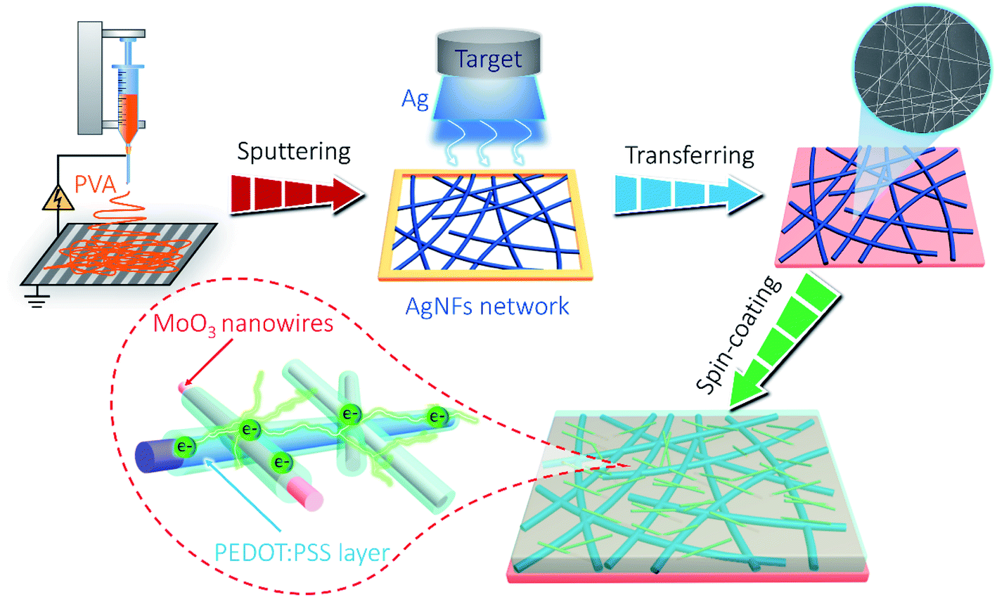 | ||
| Scheme 1 The fabrication schematic of AMP film electrodes. | ||
2. Experimental
2.1. Materials
All chemicals were of analytical grade and used without further purification. Molybdenum powder (Mo, Tianjin Guangfu Technology Development Co. Ltd), hydrogen peroxide with 30 wt% (H2O2, Chengdu Kelong Chemical Reagent Factory), sodium sulfate (Na2SO4, Chengdu Kelong Chemical Reagent Factory), lithium chloride (LiCl, Chengdu Kelong Chemical Reagent Factory), polyvinyl alcohol (PVA1788, 99.0%, Sigma-Aldrich), PEDOT:PSS and polyethylene terephthalate (PET) substrates were used for electrode fabrication and electrochemical characterization. PEDOT:PSS (1.3–1.7 wt%) was purchased from Cool Chemical Tech Co., China. The high purity silver target (99.99%) was purchased from Sino Connaught New Material Tech Co., China.2.2. Electrode preparation
:PEDOT:PSS solution = 3:1–8:1). It was found that the optimal ratio was 6:1. The AMP film electrode was obtained by spin-coating twice the above-depicted hybrid dispersion on the flexible transparent AgNF network. AgNFs/MoO3 (AM) and AgNFs/PEDOT:PSS (AP) film electrodes were also fabricated with the same process, using the MoO3 dispersion and diluted PEDOT:PSS solution (deionized water:PEDOT:PSS solution = 6:1), respectively. Finally, all film electrodes were heated at 120 °C for 30 min.
2.3. FTSC fabrication
Transparent PVA/LiCl gel electrolyte was synthesized as follows: 3 g of LiCl and 3 g of PVA were separately added into 30 mL of deionized water, and then heated to 80 °C under vigorous stirring. PVA/LiCl gel electrolyte was cast onto the AMP electrodes. Once the excess water was vaporized, a pair of film electrodes were pressed together to assemble into a symmetric sandwich-structured FTSC device. The fabrication process of the AMP-based FTSCs is illustrated in Scheme 1.2.4. Characterization
The sample structure was characterized using an X-ray diffraction spectrometer (XRD, X'pert pro, Philips) with Cu Kα radiation (range: 10–70°, step: 0.02° s−1, wavelength: 0.15406 nm) and micro Raman spectroscopy (JY-HR800 micro-Raman, using a 532 nm wavelength YAG laser with a laser spot diameter of ∼600 nm and power attenuator of D 0.3). Scanning electron microscopy (SEM, Tescan Mira3) and high-resolution transmission electron microscopy (HRTEM, FEI Tecnai G2 F30) were used to check the morphology and microstructure. An ultraviolet-visible spectrophotometer (U-3900H, HITACHI) recorded the transmittance spectra of film electrodes and devices. The elements and chemical valences were checked on an X-ray photoelectron spectrometer (XPS, PHI-5702, Mg KR X-ray, 1253.6 eV). The bending test of film electrodes and FTSC devices was performed on a measurement system assembled with an electric platform (SJH-500) and KEITHLEY2700.2.5. Electrochemical measurements
The electrochemical properties of film electrodes were characterized using an electrochemical workstation (CHI 660E) in a three-electrode configuration. The as-prepared film electrode, platinum sheet, and Ag/AgCl electrodes were used as the working, counter, and reference electrodes, respectively. The electrolyte was 2 M Na2SO4 aqueous solution. The electrochemical properties of FTSC devices were measured in a two-electrode configuration.3. Results and discussion
Fig. 1 shows the characterization of the AgNF network and MoO3 nanowire nanostructures. A randomly orientated centimeter-wide AgNF network was achieved by sputtering metallic Ag on freestanding electro-spun PVA nanofibers (Fig. 1a, S1, and S2†). After the removal of the PVA template, Ag hollow fibers with ∼65 nm wall thickness can be seen in Fig. 1a and the inset. The enlarged SEM image in Fig. 1b shows one typical AgNF junction, which largely determines the resistance of the transparent conductive electrodes (TCEs). A close contact generally leads to small sheet resistances of the TCEs. The mean diameter of the obtained AgNFs is found to be 480 nm (Fig. 1c). The hydrothermally synthesized MoO3 nanowires (Fig. 1d) are 7.9 μm in length and 240 nm in diameter (Fig. S3†). As shown in Fig. 1e, the HRTEM image of MoO3 nanowires reveals apparent lattice fringes with a spacing distance of 0.35 nm, corresponding to the (002) plane of the α-MoO3 phase (JCPDS No. 05-0508).43 Moreover, the selected area electron diffraction (SAED) pattern indicates that the as-synthesized MoO3 nanowires are monocrystalline (see the inset in Fig. 1e).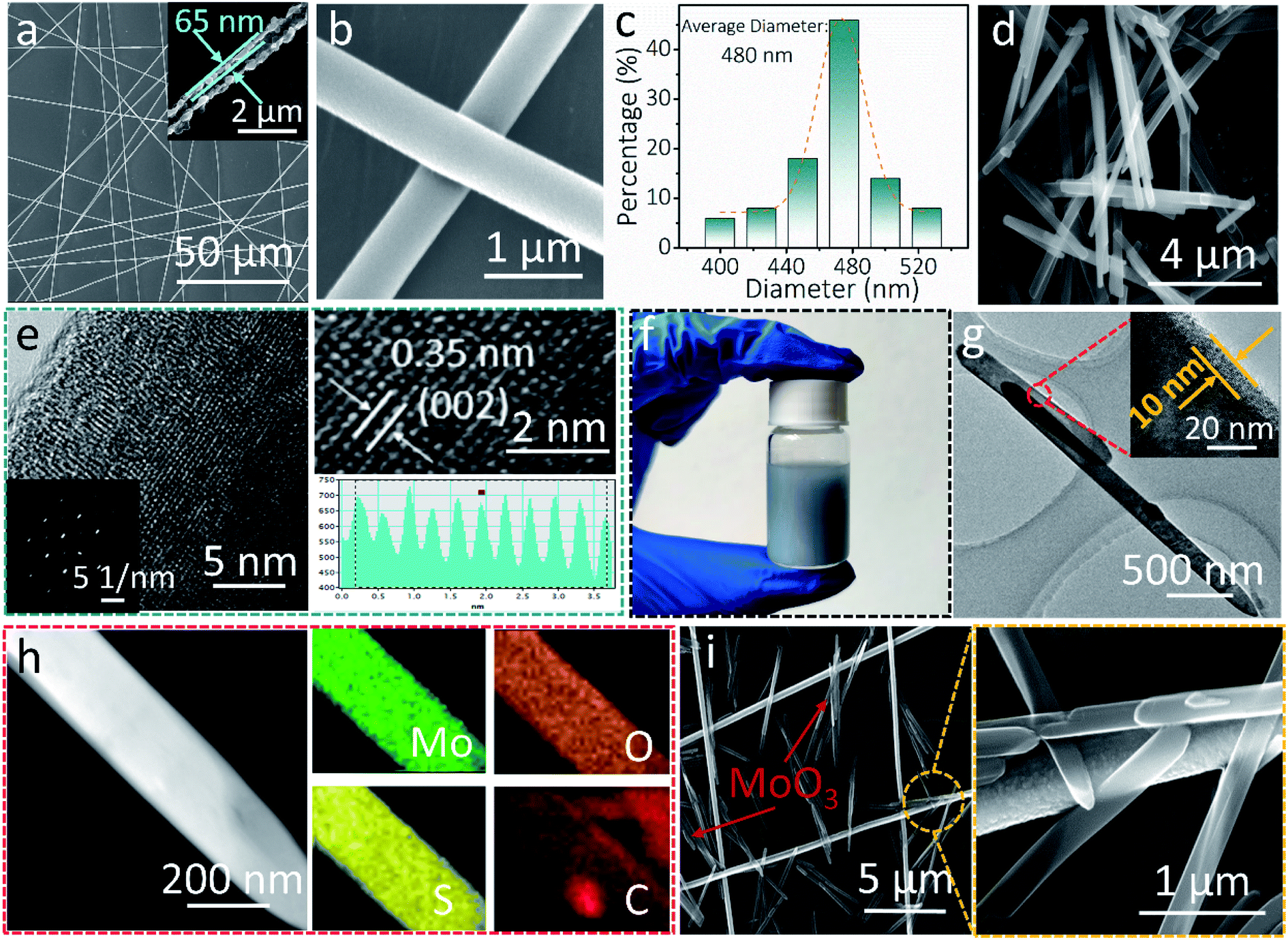 | ||
| Fig. 1 (a) and (b) SEM images of the AgNF network (inset: SEM image of AgNFs after removing PVA). (c) Diameter histogram of AgNFs. (d) SEM, (e) TEM, and HRTEM images of the as-synthesized MoO3 nanowires, the inset shows a SAED pattern. (f) Digital image of the MoO3/PEDOT:PSS dispersion. (g) TEM, HRTEM, and (h) elemental-mapping images of PEDOT:PSS-glued MoO3 nanowires. (i) SEM image of the AMP electrode. | ||
Fig. 1f shows the digital image of the MoO3/PEDOT:PSS hybrid aqueous dispersion. The TEM image of the AMP electrode shows a uniform PEDOT:PSS conducting glue layer with a thickness of 10 nm covering the surface of MoO3 nanowires (Fig. 1g). The PEDOT:PSS coating “glue” not only provides electron transport pathways and partial capacitance to maximize the charge storage capability but also reduces the contact resistance between the AgNF network and MoO3 nanowires. The element mapping in Fig. 1h shows that PEDOT:PSS-glued MoO3 nanowires contain Mo, O, C, and S elements, confirming the successful coating of an ultrathin PEDOT:PSS layer on AMP electrodes. The elemental mapping of MoO3 nanowires only shows Mo and O elements (Fig. S4†), which also proves the ultrathin PEDOT:PSS layer in the AMP electrodes compared to Fig. 1h. With the assistance of the centrifugal force during the spin-coating, MoO3 nanowires are firmly anchored on a continuous AgNFs network (Fig. 1i and S5†). One should note that a few MoO3 nanowires distributed in the interspaces can be connected to the developed AgNF network by PEDOT:PSS to build the integrated film electrode, implying higher utilization of active materials for sequent energy storage compared to the case without PEDOT:PSS “conducting glue”.
The XRD pattern (Fig. 2a) and Raman spectrum (Fig. 2b) further verify the formation of the α-MoO3 phase (JCPDS No. 05-0508).15,44 According to the XRD data analysis of Fig. 2a, the crystallite size of the MoO3 nanowire is 39.51 nm. The apparent Raman peaks can be well indexed to the Ag (159, 336, 364, 468, 819 and 997 cm−1), B1g (159, 336, 379, 468, 819, and 997 cm−1), B2g (290 and 666 cm−1), and B3g (129, 245, 290, and 666 cm−1) vibration modes of α-MoO3.45,46 As schematically illustrated in Fig. 2c, α-MoO3 is composed of a bilayer network of edge-sharing MoO6 octahedra, and these bilayers are piled up along the c-axis and bonded to adjacent layers by van der Waals forces.44 The layered crystal structure is usually suitable for intercalation/de-intercalation of ions with a relatively small ion radius, such as H+, Li+, and Na+.47 The wide-range XPS survey of PEDOT:PSS-glued MoO3 nanowires is presented in Fig. S6,† indicating the coexistence of Mo, O, and S elements. The binding energy of Mo 3d5/2 and Mo 3d3/2 electron peaks, centered at 232.6 and 235.7 eV, suggests a +6 oxidation state of Mo that is consistent with α-MoO3 (Fig. 2d and S7†).48Fig. 2e exhibits the S 2p core level spectrum, where the peaks located at 167.8 (S 2p3/2) and 163.5 eV (S 2p1/2) can be assigned to the sulfur in PEDOT:PSS chains.49,50 Besides, the O 1s spectrum can be deconvoluted into three appropriate peaks (Fig. 2f). The peak at 530.4 eV corresponds to the bridging oxygen of Mo–O–Mo,51 whereas the other two peaks at 532.2 and 532.8 eV can be attributed to the oxygen of PEDOT:PSS chains.49 All these results confirm the successful fabrication of AMP electrodes.
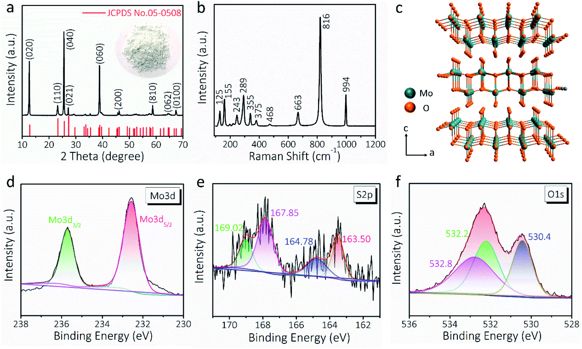 | ||
| Fig. 2 (a) XRD pattern and (b) Raman spectrum of the as-synthesized MoO3 nanowires (inset: a digital image of as-synthesized MoO3 nanowire powder). (c) Schematic diagram of the α-MoO3 crystal structure. XPS spectra of (d) Mo 3d, (e) S 2p, and (f) O 1s for PEDOT:PSS-glued MoO3 nanowires. | ||
The transparency, conductivity, mechanical flexibility, and electrical stability of the AMP electrode determine the optoelectronic and electrochemical performances of FTSCs. Fig. 3a presents the optical images of the as-prepared transparent AgNF electrode, AMP electrode, and FTSC device, respectively, demonstrating high optical transmittance in all samples. Depositing MoO3/PEDOT:PSS onto the AgNF network reduces the transmittance of the latter from 93.6% to 82.8% (at 550 nm, Fig. 3b) at the cost of slightly increased sheet resistance (from 8.0 Ω sq−1 to 9.7 Ω sq−1). The excellent optoelectronic properties (in particular the highly conductive network) can be well attributed to the unique 1D nanofibers/nanowire hybrid electrode structure assisted by the “conducting glue” at the junctions. The as-assembled FTSC device shows a transmittance of 64.5%, which is comparable to those of other reported FTSCs.2,13,52 It is worth noting that the overall optical transmittance can be further improved by reducing the distribution density or diameter of AgNFs, and/or exploring active materials with low optical conductivity.
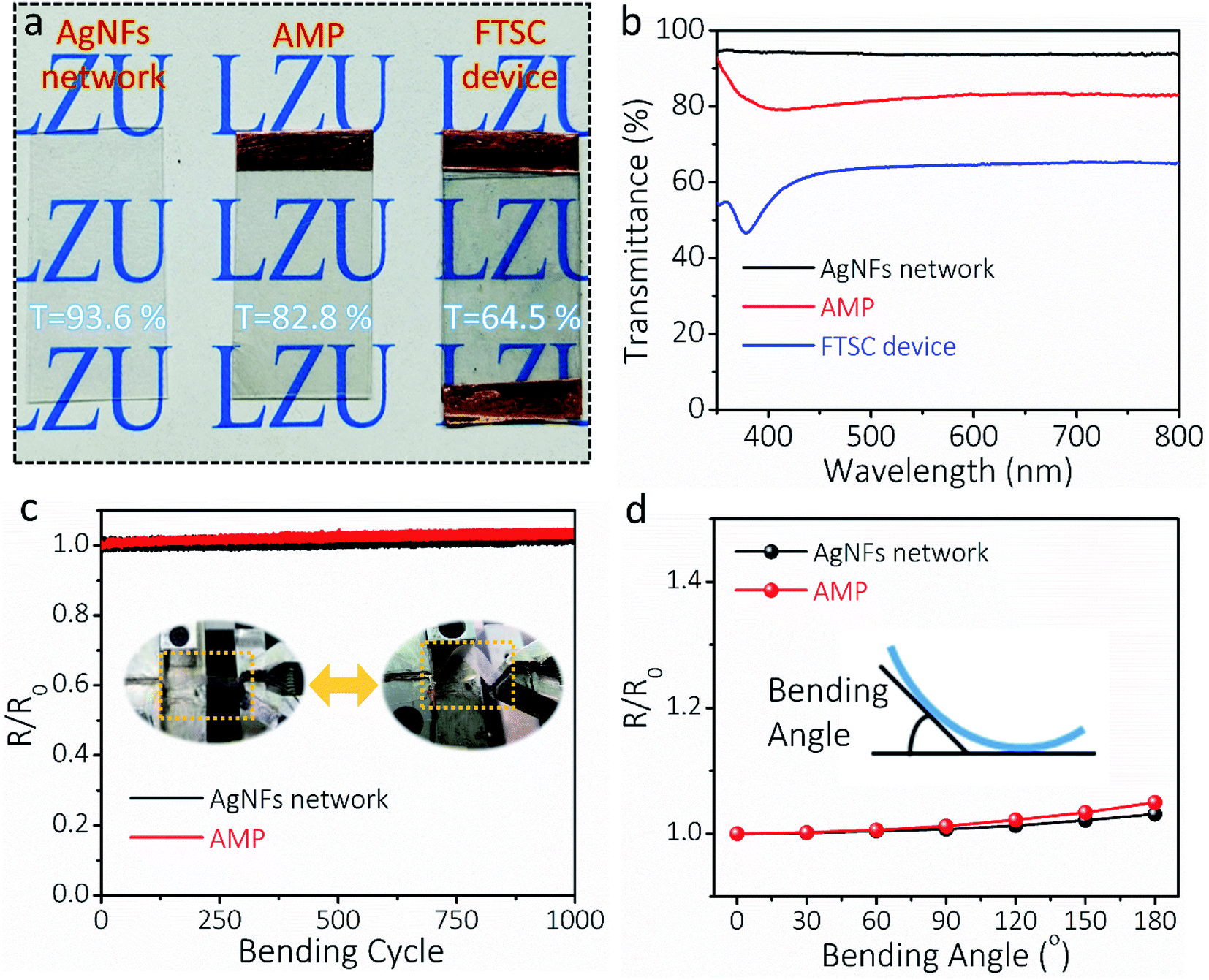 | ||
| Fig. 3 (a) Digital photographs and (b) transmittance spectra of the AgNF network, AMP electrode and FTSC device, indicating high optical transparency. (c) The relative electrical resistance of the AgNF network and AMP electrode as a function of bending cycles (inset: the bending photograph of AMP electrode). (d) The relative electrical resistance of the AgNF network and AMP electrode as a function of bending angles (inset: bending angle diagram). | ||
The AgNF network, as a current conductor in a circuit, is capable of continuously maintaining a stable LED light during the deformation (Fig. S8†). To demonstrate the flexibility of the as-fabricated TCEs, the relative resistance (R/Ro) of the electrodes is recorded as a function of bending cycles in Fig. 3c. Even after 1000 cycles (bending angle of 90°, curvature radius of 10 mm), the resistance of the AgNF network and AMP electrode remained almost unchanged, indicating superior mechanical flexibility. Moreover, R/Ro values at different bending angles were collected for the AgNF network and AMP electrode (Fig. 3d), showing that the electrical resistance remains extremely stable below the bending angle of 120°, which corresponds to a curvature radius of 6 mm. These results suggested that even after depositing MoO3/PEDOT:PSS, the flexibility of the ultrathin TCEs has been well maintained. Even bending to 180° (a curvature radius of 2 mm), the resistance of the AMP electrode increases slightly, which can be credited to the role of the conducting glue at the junctions. Notably, the mechanical flexibility of the AMP electrode is much better and the resistance change of the AMP electrode after 1000 bending cycles is much smaller compared to those of previously reported metal network/grid based on Cu nanofibers,53 AgNWs/PEDOT:PSS,54 and Ag grid,55,56 respectively (Table S1†).
The optical transparency and electrochemical properties of AMP electrodes were optimized by adjusting the volume ratio of MoO3 nanowire dispersion to PEDOT:PSS solution. Fig. 4a shows the transmittance spectra of AMP electrodes with different ratios from 3:1 to 8:1. The optical transmittance at 550 nm reduces with increasing the precursor ratio (Fig. S9†). The GCD curves at 0.10 mA cm−2 for AMP electrodes with different precursor ratios are shown in Fig. 4b. Fig. 4c shows the calculated areal capacitance at 0.10 mA cm−2 and FoMc values for the AMP electrodes with different precursor ratios. As the precursor ratio increases, the calculated areal capacitance by GCD curves reaches a peak value at 6:1 (Fig. 4b). A large precursor ratio corresponds to a lower amount of PEDOT:PSS in film electrodes, reducing the electrical conductivity of film electrodes. For transparent AMP film electrodes, the FoMc is calculated by the ratio of volumetric capacitance to optical conductivity (CV/σop).19
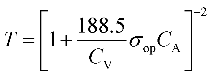 | (1) |
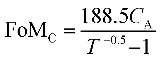 | (2) |
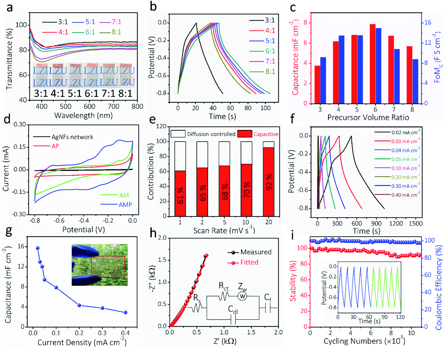 | ||
| Fig. 4 Electrochemical characterization of flexible transparent AMP electrodes. (a) Optical transmittance of the film electrodes based on different precursor ratios of MoO3 nanowires to PEDOT:PSS (inset: digital photographs of film electrodes). (b) GCD curves at 0.10 mA cm−2 for AMP electrodes with different precursor ratios. (c) Areal capacitances calculated from GCD curves and FoMc values for the electrodes with different precursor ratios. (d) CV curves at 10 mV s−1 for the AgNF network, AP, AM, and AMP film electrodes with the optimal 6:1 ratio. (e) Normalized contribution ratio of capacitive capacitance at different scan rates. (f) GCD curves measured at different current densities for the AMP electrode (precursor ratio of 6:1). (g) The calculated areal capacitance of AMP electrodes at different current densities (inset: digital photograph of AMP electrode). (h) EIS curves of AMP electrodes, the inset is an equivalent circuit diagram. (i) The electrochemical cycling stability and coulombic efficiency of AMP electrodes, the inset shows the GCD curves of the initial and final five cycles. | ||
A larger FoMc value means better charge storage capability in FTSCs at a given thickness. The AMP electrodes with the precursor ratio of 6:1 have the highest FoMc of 14.96 F S cm−2. Notably, this value is substantially higher than that of PEDOT:PSS films (1.73 F S cm−2),12 MnO2/Au electrodes (7.21 F S cm−2),38 and Co3O4/ITO electrodes (10.2 F S cm−2).57 Therefore, the optimal 6:1 ratio is utilized to evaluate the electrochemical performance of AMP electrodes, unless specifically noted. The transmittance and electrochemical performance of the film electrodes with different spin-coating times, corresponding to different amounts of active materials, are shown in Fig. S10.† Apparently, the contribution from pure AgNFs is negligible, best evidenced by the small CV integrated area compared to those of AMP electrodes (Fig. S10a†). Fig. S11† demonstrates the CVs and the derived capacitance of the AgNF electrode, showing a negligible capacitance (∼0.11 mF cm−2) from this TCE that is two orders of magnitude lower than that of AMP electrodes.
To estimate the capacitance contribution of each component in AMP electrodes, cyclic voltammetry (CV) curves (Fig. 4d) of AM, AP, and AMP film electrodes were measured at 10 mV s−1, showing areal capacitances of 2.3, 4.2, and 9.4 mF cm−2, respectively (Fig. 4d). The CV curves and areal capacitances of AM electrodes at different scan rates are shown in Fig. S12.† Besides, an apparent polarization can be observed in the CV curves of AP and AM electrodes, respectively. As the conducting glue-PEDOT:PSS is connected with more MoO3 nanowires, the AMP electrode shows higher areal capacitances majorly contributed by MoO3 instead of PEDOT:PSS. The AMP electrode exhibits a quasi-rectangular CV shape due to the synergistic influence of PEDOT:PSS and MoO3 nanowires, rendering optimal electronic and ionic transport kinetics. Based on the CV curves of the AMP electrode (Fig. S13†), the potential window of −0.8 to 0 V was selected, where the quasi-rectangular shape of the CV curve is maintained without any obvious electrochemical polarization. At the same time, this voltage window is suitable for PEDOT:PSS, since the PEDOT:PSS typically oxidizes during anodic scanning in a high voltage window.
The quasi-rectangular shape of CV curves is maintained up to 100 mV s−1 (Fig. S14†), indicating excellent capacitive behavior and reversible redox reactions. The Faraday redox reactions of MoO3 nanowires in Na+ aqueous electrolyte include surface adsorption/desorption (eqn (3)) and intercalation/deintercalation of Na+ in the interlayer spacing of MoO3 (eqn (4))47,58
| (MoVIO3)surface + Na+ + e− ↔ (MoVO3Na)surface | (3) |
| xNa+ + yH2O + MoO3 + xe− ↔ Nax+(H2O)y[MoO3]x− | (4) |
The electrochemical kinetics of AMP electrodes can be analyzed by the given relationship: i = avb, where a and b are adjustable parameters.59 When b = 0.5, the electrochemical process majorly relies on the diffusion-controlled process, while b = 1.0 indicates a capacitive process. Based on the linear relationship between log(i) and log(ν), we obtained a b-value of 0.83, implying that the capacitive process plays a leading role in the charge storage of AMP electrodes (Fig. S15†). To further analyze the capacitive and diffusion-controlled contributions at different scan rates, the current (i) can be divided into two parts: capacitive effect ( ) and diffusion-controlled reaction (
 ).60Fig. 4e shows the calculated capacitive and diffusion-controlled capacitance contributions at different scan rates. At 5 mV s−1, 68% of the total charge can be assigned to the capacitive process (Fig. S16†). The contribution from the capacitive-controlled process steadily increases with the enhancement of scan rates, which becomes dominant up to 20 mV s−1.
GCD curves and the derived capacitances at different current densities for the AMP electrode are shown in Fig. 4f–g. The maximum areal capacitance is 15.7 mF cm−2 at 0.02 mA cm−2, which is much higher than those of the previously reported FTSC electrodes, such as graphene,13 PEDOT:PSS/metal mesh,61 Co(OH)2/AgNWs,2 MnO2/metal mesh,30 and MXenes24 at similar optical transparency. Electrochemical impedance spectroscopy (EIS) was carried out to explore the ion diffusion/transport capability and electrical conductivity of AMP electrodes. As shown in Fig. 4h, the extracted equivalent series resistance (Rs) value is as low as 6.5 Ω, which proves the outstanding electrical transport behavior of AMP electrodes. Also, the steep curve in the low-frequency range suggests excellent electrochemical capacitive behavior. The long-term stability of AMP electrodes is evaluated through the GCD test at 0.30 mA cm−2, showing a capacitance retention of 92.4% after 11000 charge/discharge cycles (Fig. 4i). The inset in Fig. 4i compares the GCD curves of the initial five cycles (blue) and the final five ones (green), confirming the excellent stability of the electrode. The excellent cycling performance could be attributed to (i) the unique nanofibers/nanowire hybrid electrode structure, which guarantees the optimal electronic/ionic transport kinetics, and (ii) PEDOT:PSS conducting glue, covered on MoO3 nanowires, which effectively ensures an excellent electrical contact between MoO3 nanowires and the AgNF current collector and maximizes the charge storage capability. Furthermore, the coulombic efficiency of AMP electrodes is close to 100%, implying the absence of any parasitic reactions during repeated GCD cycles.
To demonstrate the potential of AM and AMP electrodes in practical applications, all-solid-state symmetric FTSCs were assembled with PVA/LiCl as the gel electrolyte and separator. Fig. 5a presents the CV curves of the AMP-based FTSC device measured varying from 10 to 100 mV s−1. The almost quasi-rectangular CV shapes are well maintained up to 100 mV s−1, indicating pseudo-capacitive behaviors and rapid charge/discharge capability, which can also be verified by the GCD curves in Fig. 5b. The GCD curve of the FTSC device measured with a potential window of 0 to 0.8 V under different applied current densities exhibited a typical symmetric triangular shape, indicating good electrochemical capacitive characteristics (Fig. 5b). The symmetric charge/discharge curves of the device also indicate a relatively high coulombic efficiency. The areal capacitance of the FTSC is exhibited in Fig. 5c. A large areal capacitance of 7.0 mF cm−2 is achieved at 0.1 mA cm−2 of the AMP-based FTSC device, which is significantly higher than those of previously reported FTSCs.2,13,52 The areal capacitance of the AMP-based FTSC device is doubled compared to the AM-based FTSC device (Fig. S17†), highlighting the importance of PEDOT:PSS as the conducting glue. It is undeniable that PEDOT:PSS has a certain capacitance contribution. Hence, the expected combination of high transmittance and large capacitance has been achieved in our as-prepared AMP-based FTSC devices (Fig. 5d and Table S2†). The acquired EIS comparison results also demonstrate that the AMP-based FTSCs render a low internal resistance and fast ionic diffusion (Fig. S18†). Moreover, the FTSCs exhibit excellent long-term cycling stability (Fig. 5e), retaining 86.6% of the initial capacitance after 15000 charge/discharge cycles. As shown in Fig. 5f, the energy density (0.623 μW h cm−2) and power density (40 μW cm−2) of the AMP-based FTSC device have also outperformed the previously reported transparent supercapacitors, such as Ti3C2Tx films,24 PEDOT:PSS,12 RuO2/PEDOT:PSS,18 graphene quantum-dot,62 CVD-graphene63 and multilayer reduced graphene oxide thin films.63 (Table S3†) To meet practical applications, the required voltage and capacitance can be achieved via a simple serial-parallel configuration. Fig. 5g shows CV curves of a single device and two identical devices connected in either parallel or series configurations. The operated potential window can be enlarged from 0.8 to 1.6 V by connecting two devices in series, whereas the output current density (i.e. capacitance) can be increased twice by connecting two devices in parallel. Moreover, the GCD curves of tandem devices are consistent with the results of CV curves (Fig. S19†). Also, three tandem transparent devices can readily drive a multifunction thermometer (Fig. 5h), showcasing promising applications of our flexible transparent supercapacitors in powering portable electronics. Besides, the CV curves of the AMP-based FTSC device were measured at 50 mV s−1 when the device was bent at different angles (Fig. S20†). After 100 bending cycles at 90° (Fig. 5i), almost no decrease in capacitance was observed, implying the robust nature of our fabricated transparent solid-state devices. These attractive properties, including the very high figure of merit (charge storage), excellent optoelectronic properties in combination with mechanical resilient and electrochemical performances, suggest the great promise of AMP-based FTSCs in next-generation transparent, wearable electronics.
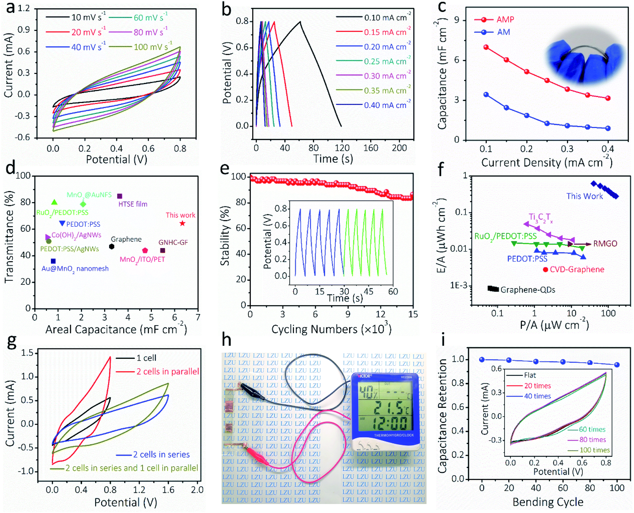 | ||
| Fig. 5 Electrochemical characterization of the assembled all-solid-state FTSCs based on AMP electrodes. (a) CV curves at different scan rates and (b) GCD curves at different current densities for the AMP-based FTSCs. (c) The calculated areal capacitance obtained from GCD curves (inset: digital photograph of the AMP-based FTSC device). (d) The areal capacitance and optical transmittance compared with the other reported FTSCs. The detailed values are presented in Table S2.† (e) Electrochemical cycling stability of the FTSC, the inset shows the GCD curves of the initial and the final five cycles. (f) Ragone plots of the FTSC, compared with the other reported ones. The detailed values are presented in Table S3.† (g) CV curves of the FTSC devices at different configurations. (h) A digital photograph showing that three FTSCs in series can power a multifunction thermometer. (i) The electrochemical performance of the FTSC device during the bending, the inset shows CV curves of the FTSC at 50 mV s−1 after different bending times. | ||
4. Conclusions
In summary, we have designed an AMP film electrode for an advanced transparent, flexible supercapacitor device. The PEDOT:PSS functions as “conducting glue” between the highly conductive AgNF network and high-theoretical capacitance MoO3 nanowires, resulting in much enhanced electron hopping kinetics and improved mechanical adhesion of the active materials. These synergistic effects render a high areal capacitance of 15.71 mF cm−2 at an optical transparency of 82.8% in the AMP film electrodes, coupled with long-term electrochemical cycle stability (92.4% capacitance retention after 11000 charge/discharge cycles) and excellent mechanical flexibility (withstanding 1000 bending cycles). More importantly, the AMP-based all-solid-state symmetric FTSCs also exhibit large capacitance, high energy density, superior power density, and long-term cycling stability. These results indicate the great potential of nanofibers/nanowire hybrid network structures in high-performance transparent, wearable, and portable electronics.
Author contributions
Jie Liang: conceptualization, methodology, data curation, writing – original draft, investigation, visualization, validation. Hongwei Sheng: investigation, methodology, writing – review & editing. Qi Wang: investigation. Jiao Yuan: methodology. Xuetao Zhang: methodology. Qing Su: writing – review & editing. Erqing Xie: supervision. Wei Lan: writing – review & editing, funding acquisition, project administration, resources, supervision. Chuanfang (John) Zhang: conceptualization, data curation, writing – review & editing.Conflicts of interest
The authors declare no conflicts of interest.Acknowledgements
This work was supported by the National Natural Science Foundation of China (61874166 and U1832149) and the Science and Technology Program of Qinghai Province (2020-HZ-809).Notes and references
- C. F. Zhang and V. Nicolosi, Energy Storage Materials, 2019, 16, 102–125 CrossRef.
- H. Sheng, X. Zhang, Y. Ma, P. Wang, J. Zhou, Q. Su, W. Lan, E. Xie and C. J. Zhang, ACS Appl. Mater. Interfaces, 2019, 11, 8992–9001 CrossRef CAS PubMed.
- H. Zhou, Y. Zhang, Y. Qiu, H. Wu, W. Qin, Y. Liao, Q. Yu and H. Cheng, Biosens. Bioelectron., 2020, 168, 112569 CrossRef CAS PubMed.
- C. Zhang, Z. Peng, C. Huang, B. Zhang, C. Xing, H. Chen, H. Cheng, J. Wang and S. Tang, Nano Energy, 2021, 81, 105609 CrossRef CAS.
- C. F. Zhang, M. Y. Liang, S. H. Park, Z. F. Lin, A. Seral-Ascaso, L. L. Wang, A. Pakdel, C. O. Coileain, J. Boland, O. Ronan, N. McEvoy, B. G. Lu, Y. G. Wang, Y. Y. Xia, J. N. Coleman and V. Nicolosi, Energy Environ. Sci., 2020, 13, 2124–2133 RSC.
- J. Xiong, L. M. Pan, H. H. Wang, F. Du, Y. M. Chen, J. Yang and C. F. Zhang, Electrochim. Acta, 2018, 268, 503–511 CrossRef CAS.
- H. Tang, W. L. Li, L. M. Pan, K. J. Tu, F. Du, T. Qiu, J. Yang, C. P. Cullen, N. McEvoy and C. F. Zhang, Adv. Funct. Mater., 2019, 29, 1901907 CrossRef.
- G. Yasin, M. Arif, T. Mehtab, M. Shakeel, M. A. Mushtaq, A. Kumar, T. A. Nguyen, Y. Slimani, M. T. Nazir and H. H. Song, Inorg. Chem. Front., 2020, 7, 402–410 RSC.
- S. Ullah, G. Yasin, A. Ahmad, L. Qin, Q. Yuan, A. U. Khan, U. A. Khan, A. U. Rahman and Y. Slimani, Inorg. Chem. Front., 2020, 7, 1750–1761 RSC.
- Y. Slimani and E. Hannachi, in Nanobatteries and Nanogenerators, ed. H. Song, R. Venkatachalam, T. A. Nguyen, H. B. Wu and P. Nguyen-Tri, Elsevier, 2021, pp. 343–363, DOI:10.1016/B978-0-12-821548-7.00013-0.
- T. Chen, Y. Xue, A. K. Roy and L. Dai, ACS Nano, 2014, 8, 1039–1046 CrossRef CAS PubMed.
- T. M. Higgins and J. N. Coleman, ACS Appl. Mater. Interfaces, 2015, 7, 16495–16506 CrossRef CAS PubMed.
- N. Li, G. Yang, Y. Sun, H. Song, H. Cui, G. Yang and C. Wang, Nano Lett., 2015, 15, 3195–3203 CrossRef CAS PubMed.
- Y. H. Liu, J. L. Xu, S. Shen, X. L. Cai, L. S. Chen and S. D. Wang, J. Mater. Chem. A, 2017, 5, 9032–9041 RSC.
- B. Yao, L. Huang, J. Zhang, X. Gao, J. Wu, Y. Cheng, X. Xiao, B. Wang, Y. Li and J. Zhou, Adv. Mater., 2016, 28, 6353–6358 CrossRef CAS PubMed.
- K. Seevakan, A. Manikandan, P. Devendran, Y. Slimani, A. Baykal and T. Alagesan, J. Magn. Magn. Mater., 2019, 486, 165254 CrossRef CAS.
- Y. Slimani and E. Hannachi, in Hybrid Perovskite Composite Materials, eds. I. Khan, A. Khan, M. M. A. Khan, S. Khan, F. Verpoort and A. Umar, Woodhead Publishing, 2021, pp. 335–354, DOI:10.1016/B978-0-12-819977-0.00016-0.
- C. F. Zhang, T. M. Higgins, S. H. Park, S. E. O'Brien, D. H. Long, J. Coleman and V. Nicolosi, Nano Energy, 2016, 28, 495–505 CrossRef CAS.
- L. B. Wang and X. L. Hu, Batteries Supercaps, 2020, 3, 1–13 CrossRef.
- S. Sollami Delekta, A. D. Smith, J. Li and M. Östling, Nanoscale, 2017, 9, 6998–7005 RSC.
- D. S. Hecht, L. Hu and G. Irvin, Adv. Mater., 2011, 23, 1482–1513 CrossRef CAS PubMed.
- J. Ge, G. Cheng and L. Chen, Nanoscale, 2011, 3, 3084–3088 RSC.
- E. Senokos, M. Rana, M. Vila, J. Fernandez-Cestau, R. D. Costa, R. Marcilla and J. J. Vilatela, Nanoscale, 2020, 12, 16980–16986 RSC.
- C. J. Zhang, B. Anasori, A. Seral-Ascaso, S. H. Park, N. McEvoy, A. Shmeliov, G. S. Duesberg, J. N. Coleman, Y. Gogotsi and V. Nicolosi, Adv. Mater., 2017, 29, 1702678 CrossRef PubMed.
- P. Salles, E. Quain, N. Kurra, A. Sarycheva and Y. Gogotsi, Small, 2018, 14, 1802864 CrossRef PubMed.
- S. Abdolhosseinzadeh, R. Schneider, A. Verma, J. Heier, F. Nuesch and C. F. Zhang, Adv. Mater., 2020, 32, 2000716 CrossRef CAS PubMed.
- C. F. Zhang, L. F. Cui, S. Abdolhosseinzadeh and J. Heier, Infomat, 2020, 2, 613–638 CrossRef CAS.
- S. Abdolhosseinzadeh, J. Heier and C. F. Zhang, JPhys Energy, 2020, 2, 031004 CrossRef CAS.
- A. W. Lang, Y. Y. Li, M. De Keersmaecker, D. E. Shen, A. M. Osterholm, L. Berglund and J. R. Reynolds, ChemSusChem, 2018, 11, 854–863 CrossRef CAS PubMed.
- S. B. Singh, T. I. Singh, N. H. Kim and J. H. Lee, J. Mater. Chem. A, 2019, 7, 10672–10683 RSC.
- X. Jiao, C. Zhang and Z. Yuan, ACS Appl. Mater. Interfaces, 2018, 10, 41299–41311 CrossRef CAS PubMed.
- H. Moon, H. Lee, J. Kwon, Y. D. Suh, D. K. Kim, I. Ha, J. Yeo, S. Hong and S. H. Ko, Sci. Rep., 2017, 7, 41981 CrossRef CAS PubMed.
- R. T. Wang, X. B. Yan, J. W. Lang, Z. M. Zheng and P. Zhang, J. Mater. Chem. A, 2014, 2, 12724–12732 RSC.
- H. B. Lee, W. Y. Jin, M. M. Ovhal, N. Kumar and J. W. Kang, J. Mater. Chem. C, 2019, 7, 1087–1110 RSC.
- S. Gong, Y. M. Zhao, Q. Q. Shi, Y. Wang, L. W. Yap and W. L. Cheng, Electroanal, 2016, 28, 1298–1304 CrossRef CAS.
- Y. Lee, S. Chae, H. Park, J. Kim and S. H. Jeong, Chem. Eng. J., 2020, 382, 122798 CrossRef CAS.
- Y. Wang, S. Gong, D. Dong, Y. Zhao, L. W. Yap, Q. Shi, T. An, Y. Ling, G. P. Simon and W. Cheng, Nanoscale, 2018, 10, 15948–15955 RSC.
- S. Kiruthika, C. Sow and G. U. Kulkarni, Small, 2017, 13, 1701906 CrossRef PubMed.
- S. Q. Chen, B. B. Shi, W. D. He, X. Y. Wu, X. Zhang, Y. B. Zhu, S. He, H. H. Peng, Y. Jiang, X. S. Gao, Z. Fan, G. F. Zhou, J. M. Liu, K. Kempa and J. W. Gao, Adv. Funct. Mater., 2019, 29, 1906618 CrossRef CAS.
- Y. Slimani, A. Selmi, E. Hannachi, M. A. Almessiere, M. Mumtaz, A. Baykal and I. Ercan, J. Mater. Sci.: Mater. Electron., 2019, 30, 13509–13518 CrossRef CAS.
- S. B. Singh, T. Kshetri, T. I. Singh, N. H. Kim and J. H. Lee, Chem. Eng. J., 2019, 359, 197–207 CrossRef CAS.
- T. Cheng, Y. Z. Zhang, J. D. Zhang, W. Y. Lai and W. Huang, J. Mater. Chem. A, 2016, 4, 10493–10499 RSC.
- S. Balendhran, J. Deng, J. Z. Ou, S. Walia, J. Scott, J. Tang, K. L. Wang, M. R. Field, S. Russo, S. Zhuiykov, M. S. Strano, N. Medhekar, S. Sriram, M. Bhaskaran and K. Kalantar-zadeh, Adv. Mater., 2013, 25, 109–114 CrossRef CAS PubMed.
- S. N. Lou, Y. H. Ng, C. Ng, J. Scott and R. Amal, ChemSusChem, 2014, 7, 1934–1941 CrossRef CAS PubMed.
- G. Mestl, P. Ruiz, B. Delmon and H. Knozinger, J. Phys. Chem., 1994, 98, 11269–11275 CrossRef CAS.
- J. Zhou, N. S. Xu, S. Z. Deng, J. Chen, J. C. She and Z. C. Wang, Adv. Mater., 2003, 15, 1835–1840 CrossRef CAS.
- J. B. Jiang, J. L. Liu, S. J. Peng, D. Qian, D. M. Luo, Q. Wang, Z. W. Tian and Y. C. Liu, J. Mater. Chem. A, 2013, 1, 2588 RSC.
- Z. Chen, D. Cummins, B. N. Reinecke, E. Clark, M. K. Sunkara and T. F. Jaramillo, Nano Lett., 2011, 11, 4168–4175 CrossRef CAS PubMed.
- D. A. Mengistie, M. A. Ibrahem, P. C. Wang and C. W. Chu, ACS Appl. Mater. Interfaces, 2014, 6, 2292–2299 CrossRef CAS PubMed.
- Y. Xia, K. Sun and J. Ouyang, Adv. Mater., 2012, 24, 2436–2440 CrossRef CAS PubMed.
- J. C. Dupin, D. Gonbeau, P. Vinatier and A. Levasseur, Phys. Chem. Chem. Phys., 2000, 2, 1319–1324 RSC.
- T. Qiu, B. Luo, M. Giersig, E. M. Akinoglu, L. Hao, X. Wang, L. Shi, M. Jin and L. Zhi, Small, 2014, 10, 4136–4141 CAS.
- H. Wu, L. Hu, M. W. Rowell, D. Kong, J. J. Cha, J. R. McDonough, J. Zhu, Y. Yang, M. D. McGehee and Y. Cui, Nano Lett., 2010, 10, 4242–4248 CrossRef CAS PubMed.
- R. T. Ginting, M. M. Ovhal and J. W. Kang, Nano Energy, 2018, 53, 650–657 CrossRef CAS.
- S. Hong, J. Yeo, G. Kim, D. Kim, H. Lee, J. Kwon, H. Lee, P. Lee and S. H. Ko, ACS Nano, 2013, 7, 5024–5031 CrossRef CAS PubMed.
- Y. Lee, W. Y. Jin, K. Y. Cho, J. W. Kang and J. Kim, J. Mater. Chem. C, 2016, 4, 7577–7583 RSC.
- X. Y. Liu, Y. Q. Gao and G. W. Yang, Nanoscale, 2016, 8, 4227–4235 RSC.
- I. Shakir, M. Nadeem, M. Shahid and D. J. Kang, Electrochim. Acta, 2014, 118, 138–142 CrossRef CAS.
- J. Liu, J. Wang, C. Xu, H. Jiang, C. Li, L. Zhang, J. Lin and Z. X. Shen, Adv. Sci., 2018, 5, 1700322 CrossRef PubMed.
- H. S. Kim, J. B. Cook, H. Lin, J. S. Ko, S. H. Tolbert, V. Ozolins and B. Dunn, Nat. Mater., 2017, 16, 454–460 CrossRef CAS PubMed.
- X. Liu, D. Li, X. Chen, W. Y. Lai and W. Huang, ACS Appl. Mater. Interfaces, 2018, 10, 32536–32542 CrossRef CAS PubMed.
- K. Lee, H. Lee, Y. Shin, Y. Yoon, D. Kim and H. Lee, Nano Energy, 2016, 26, 746–754 CrossRef CAS.
- J. J. Yoo, K. Balakrishnan, J. Huang, V. Meunier, B. G. Sumpter, A. Srivastava, M. Conway, A. L. Reddy, J. Yu, R. Vajtai and P. M. Ajayan, Nano Lett., 2011, 11, 1423–1427 CrossRef CAS PubMed.
Footnote |
| † Electronic supplementary information (ESI) available. See DOI: 10.1039/d1na00121c |
| This journal is © The Royal Society of Chemistry 2021 |