
 Open Access Article
 This Open Access Article is licensed under a Creative Commons Attribution-Non Commercial 3.0 Unported Licence
Tunable conductance and spin filtering in twisted bilayer copper phthalocyanine molecular devices
Jian-Hua
Liu
 ab,
Kun
Luo
ab,
Kailiang
Huang
ab,
Bing
Sun
ab,
Shengli
Zhang
*c and
Zhen-Hua
Wu
*ab
ab,
Kun
Luo
ab,
Kailiang
Huang
ab,
Bing
Sun
ab,
Shengli
Zhang
*c and
Zhen-Hua
Wu
*ab
aInstitute of Microelectronics, Chinese Academy of Sciences, Beijing 100029, China. E-mail: wuzhenhua@ime.ac.cn
bCollege of Microelectronics, University of Chinese Academy of Sciences, Beijing 100029, China
cMIIT Key Laboratory of Advanced Display Materials and Devices, School of Materials Science and Engineering, Nanjing University of Science and Technology, Nanjing 210094, China. E-mail: zhangslvip@njust.edu.cn
First published on 7th April 2021
Abstract
We investigate theoretically the quantum transport properties of a twisted bilayer copper phthalocyanine (CuPc) molecular device, in which the bottom-layer CuPc molecule is connected to V-shaped zigzag-edged graphene nanoribbon electrodes. Based on a non-equilibrium Green's function approach in combination with density-functional theory, we find that the twist angle effectively modulates the electron interaction between the bilayer CuPc molecules. HOMO (highest occupied molecular orbital)–LUMO (lowest unoccupied molecular orbital) gap, spin filtering efficiency (SFE) and spin-dependent conductance of the bilayer CuPc molecular device could be modulated by changing the twist angle. The conductance reaches its maximum when the twist angle θ is 0° while the largest SFE is achieved when θ = 60°. The twist angle-induced exotic transport phenomena can be well explained by analyzing the transmission spectra, molecular energy level spectra and scattering states of the twisted bilayer CuPc molecular device. The tunable conductance, HOMO–LUMO gap and spin filtering versus twist angle are helpful for predicting how a two-molecule system may behave with twist angle.
1. Introduction
Metal phthalocyanines have attracted widespread attention in the past decade, and more and more experimental and theoretical researches have been developed for their high stability, rich thermal and electrical properties, and easily modified electronic structure and spin state by changing the central atom.1–7 Molecular spintronic devices will play a key role in nanoelectronics. The bilayer system exhibits a diversity of spin-related phenomena8–11 and twistronics12 has become a hotspot in research of bilayer two-dimensional materials for which manipulating the electronic behaviours can be achieved by rotating the relative orientation of adjacent layers. The spatial localizations of electronic states lead to Moire bands,13–15 topological features,16–18 insulated states19–21 and unconventional superconductivity22,23 due to strong correlations and interlayer coupling in Moire superlattices formed by small-angle twisted layered 2D systems.24 The spin orientation in a 3D topological insulator can be tuned by changing the incident angles.25 The carrier transport properties can be tuned dramatically by periodic magnetic fields and Rashba spin–orbit coupling.26 The conductance of a topological insulator quantum dot can be tuned by changing the Fermi energy, the width of the topological insulator constrictions and the quantum well bandgap.27 However, there is no systematic research of the twist angles of molecular devices.In this paper, based on non-equilibrium Green's function (NEGF) in combination with density-functional theory (DFT),28,29 we study the quantum transport property of a CuPc molecular device consisting of a CuPc molecule with different twist angle linked by two V-shaped zigzag-edged graphene nanoribbon (GNR) electrodes. We can control the local spin states and associated quantum transport property of the device by changing the twist angle. The results show that HOMO–LUMO gap, spin filter efficiency (SFE) and spin-dependent conductance of the twisted bilayer CuPc molecules (TTBCPM) vary with the twist angle. The change trend of conductance and SFE is almost opposite for large θ. The conductance is at its maximum for θ = 0° and the largest SFE is at θ = 60°. Physical mechanisms are proposed for these phenomena and the quantum transport phenomenon with twist angle is further understood by analysing the transmission spectra, molecular energy level spectra and scattering states.
2. Computational details
We investigate the transport properties of a twisted bilayer CuPc molecule device (TTBCPMD) by using DFT combined with the Keldysh NEGF formalism, as implemented by the Nanodcal transport package.30Fig. 1(a) and (b) show top and side views of the structure of the TTBCPMD. In the horizontal plane, we rotate the top CuPc around the central Cu atom by an angle θ relative to the fixed bottom CuPc. The device consists of three parts: left and right electrodes (which extend to ±∞) and central scattering region, which contains twisted bilayer CuPc molecules, and left and right buffer layers. The left and right GNRs are symmetrically connected to the two carbon atoms of the left and right benzenes of the bottom CuPc molecule, respectively. The top CuPc molecule is situated horizontally above the bottom CuPc molecule. The cutoff energy is set to be 150 Rydberg, electrode temperature is chosen to be 300 K and the k-point grid is set to be 100 × 1 × 1. Electrodes of ZGNRS of 8 atoms in width are considered with a supercell (4.9332 × 27.821 × 13 Å) subjected to periodic boundary conditions. We introduce a vacuum layer of about 10 Å in y direction and z direction to eliminate interaction between GNRs and bilayer CuPc molecule in neighboring cells, and the edge atoms, both electrodes and the central region are saturated with hydrogen (H) atoms to remove the dangling bonds.7 The exchange–correlation function is described by the local density approximation proposed by Perdew and Zunger. The structures are not relaxed because perfect twist angle structure without relaxation can help us to more clearly obtain the physics induced by angles between the bilayer CuPc molecules.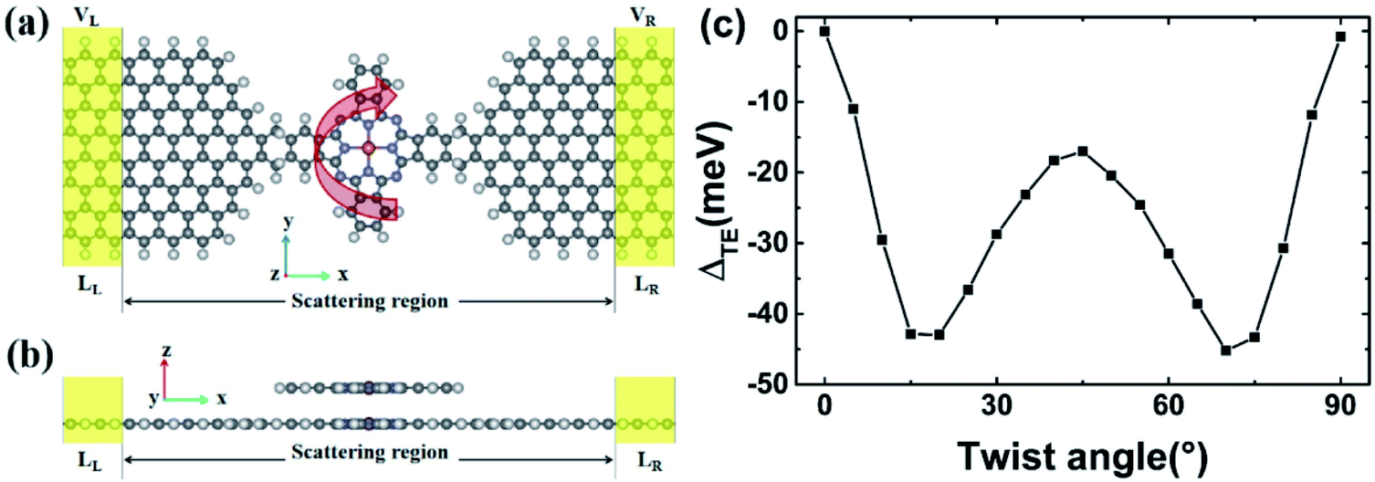 | ||
| Fig. 1 The structure of the TTBCPMD. The red, blue, black, and grey spheres represent Cu, N, C, and H atoms, respectively. The molecule in the scattering region is CuPc, the electrodes are V-shaped zigzag-edged GNRs. (a) and (b) are top and side views of the molecular device. (c) The difference between the total energy of TTBCPMD with twist angle θ and the untwisted reference, i.e., θ0 = 0°. | ||
The spin-polarized zero-bias conductance is given by the Landauer–Buttiker formula31 as
 | (1) |
| Tσ(EF) = Tr[ΓLGRΓRGA], | (2) |
 and GR = [GA]†, Hc is the Hamiltonian matrix for the scattering region of the device, Sc is the overlap matrix, and
  and
and  are the retarded self-energy of the left and right lead.
Under equilibrium states, SFE is defined as

| (3) |
Scattering states are the eigenstates of the open two-terminal device structure linking z = −∞ to z = +∞ and are useful for analyzing the transport properties of the device.30,32,33
3. Results and discussion
We considered the twist angle from 0° to 90° because of the structural symmetry of the TTBCPMD.Fig. 1(c) shows the difference in total energy ΔTE between the TTBCPMD of twist angle θ and the untwisted reference, i.e., ΔTE = TEθ − TE0, which shows that if ΔTE is small, TEθ is small. We can find that the total energy for θ = 0° is the highest and the total energy for θ = 70° is the lowest, which correspond to the largest and least total conductance for θ = 0° and θ = 70°. The copper atom in the CuPc molecule forms a bond with the N atoms along the transport direction, and the distance is bigger than the distance between the copper atom and the N atoms in the lateral direction shown in Fig. 1(a). The asymmetry of the structure causes the interaction between the upper and lower CuPc molecules to be different when the twist angle is 20° and 70°, so there will be an energy difference between the twist angles of 20° and 70°.
Fig. 2(a) shows that the spin-dependent conductance varies with twist angle θ. The left inset shows the total conductance (total G), spin-up (SU, black-line) conductance and spin-down (SD, red-line) conductance for θ = 0–10°. The total G and SD conductance show a downward trend for θ = 0–20°, 30–40°, 55–70° and an upward trend for θ = 20–30°, 40–55°, 70–90°. The SU conductance in the right inset shows clearly a downward trend for θ = 0–30°, 45–60° and an upward trend for θ = 30–45°, 60–90°, which corresponds to the change of transmission at the Fermi level with different twist angle θ. We focus on the transmission at the Fermi level with θ = 10°, 20°, 30°, 40° and 45° since the trend of conductance versus θ is almost symmetric with respect to θ = 45°. The inset shows the transmission with dense energy points of the device versus θ. At the Fermi level, the transmission decreases when θ goes from 10° to 20° and from 30° to 40°, and increases when θ goes from 20° to 30° and from 40° to 45° in the SD channel shown in Fig. 2(b). The above trend of the transmission corresponds to the change of the SD conductance. The transmission in the SU channel decreases when θ goes from 10° to 30° and increases when θ goes from 30° to 45° in Fig. 2(b), which corresponds to the change of the SU conductance, and it can be described by eqn (1) when the devices are under equilibrium states and summed along the x-direction.
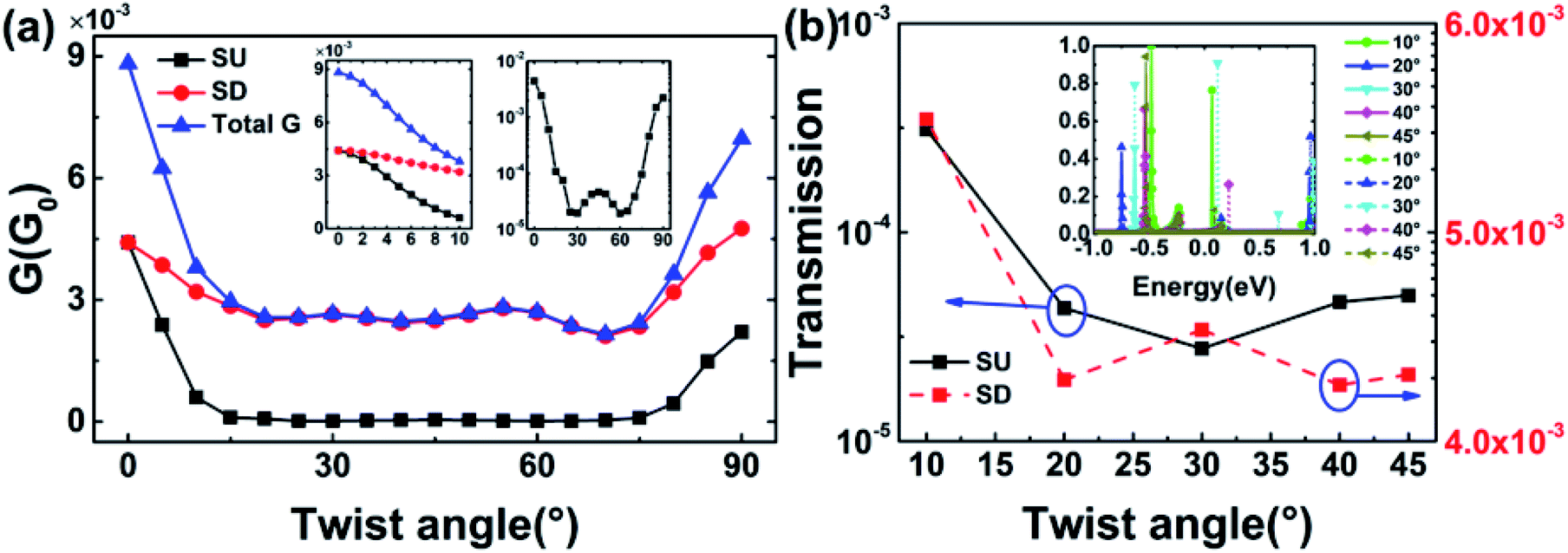 | ||
| Fig. 2 The spin-dependent conductance G (a) and spin-polarized transmission spectra (b) at zero bias of the TTBCPMD vary with the twist angle. | ||
The SFE reaches its maximum at θ = 25° and 60°. This can be understood by analyzing the spin-polarized transmission coefficient at the Fermi level at zero bias. Fig. 3 shows that SFE > 87% and T↑ ≪T↓, which indicates that the SD channel mainly determines the SFE. Therefore, we should use an appropriate value of θ to obtain larger conductance and SFE to improve the practicability of a twisted-angle bilayer CuPc molecular device in electronics and spintronics. The conductance and SFE change smoothly with θ. In order to understand these transport behaviors better, the molecular levels, HOMO–LUMO (H–L) gap and scattering states of the TTBCPMD are given in Fig. 4 and 5.
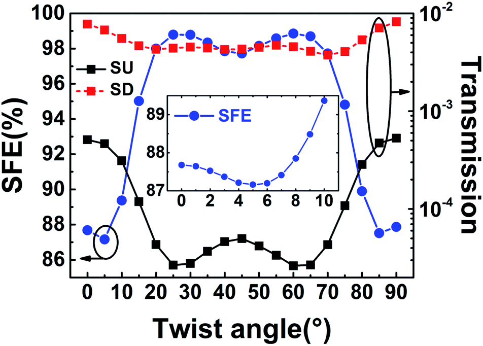 | ||
| Fig. 3 SFE and transmission coefficient at the Fermi level of the TTBCPMD vary with θ at zero bias. | ||
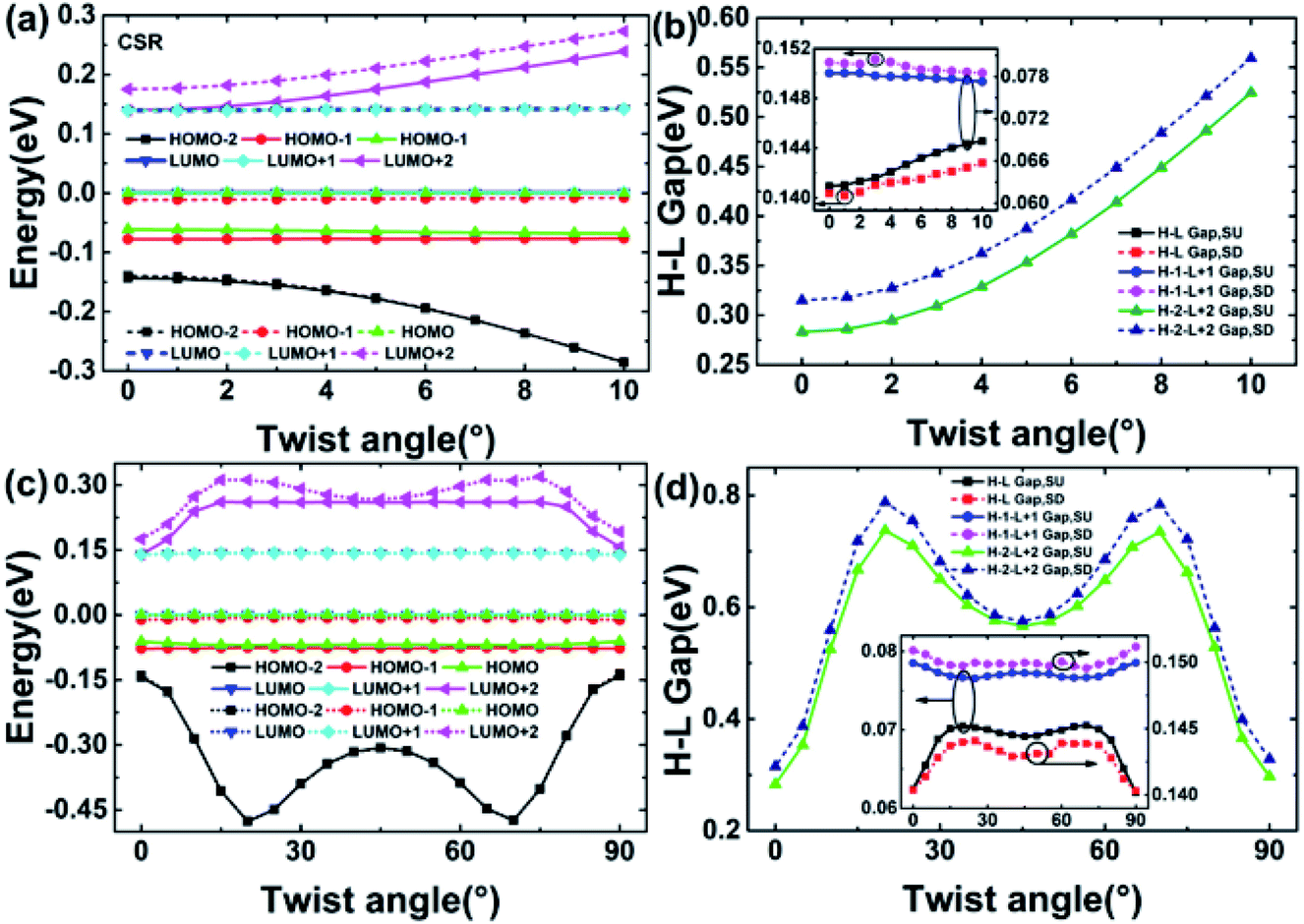 | ||
| Fig. 4 (a and c) The θ dependency of spin-up and spin-down energy spectrum of the CSR with θ = 0–10° and θ = 0–90°. (b and d) The θ dependency of HOMO–LUMO gap of the CSR with θ = 0–10° and θ = 0–90°. The Fermi level is set to zero. | ||
 | ||
| Fig. 5 Scattering wavefunction associated with incoming state of lead L and lead R of the region of TTBCPM for spin-up (a) and spin-down (b) for θ = 10–45° at zero bias voltage. | ||
To understand the underlying mechanism of the observed conductance in Fig. 2(a), we calculate the energy spectra and HOMO–LUMO gap of the center scattering region (CSR) versus twist angle θ as shown in Fig. 4. In Fig. 4(a), for the SU energy level, as the twist angle increases, HOMO−2 (H−2), HOMO and LUMO+2 (L+2) levels are far away from the Fermi level, and the H−1 level approaches the Fermi level. The L and the L+1 levels firstly approach and then move away from the Fermi level. For the SD energy level, as the twist angle increases, the H−2, the L, the L+1, and the L+2 levels are far away from the Fermi level, and the H−1 level approaches the Fermi level. The H level firstly approaches and then moves away from the Fermi level. The dependence of conductance on the twist angle is basically the opposite of the trend of the H–L gap changes. Generally, a large H–L gap corresponds to a small conductance. We find that the energy spectrum and H–L gap are nearly symmetric with respect to the line of θ = 45° in Fig. 4(d). Therefore, we only analyze the energy spectra and H–L gap in half the region, i.e., θ = 0–45°. The L+2 level and H−2 level move away from the Fermi level obviously when θ changes from 0° to 10° as shown in Fig. 4(b). The L level, the first orbital above L (L+1) level, the H level, and H−1 level in SU and SD channels change slowly with θ. The trend discussed above corresponds to the energy dispersions of SU and SD carriers in the TTBCPMD versus θ. The H−2–L+2 gap increases with θ. The H−1–L+1 gap shows a downward trend and the H–L gap shows an upward trend in SU and SD channels for θ = 0–10° in Fig. 4(b). The H−2–L+2 gap and H–L gap in the SD channel increase and the H−1–L+1 gap decreases with θ for θ = 0–20°. The energy spectra shown in Fig. 4(c), and the H−2–L+2 gap, H−1–L+1 gap, H–L gap in SU and SD channels shown in Fig. 4(d) determine the corresponding conductance in Fig. 2(a).
Fig. 5 shows the real-space scattering states of the TTBCPMD system at the Fermi energy EF and the incoming kx = 0. The scattering of incoming state 1 of lead L (S1LL) and lead R (S1LR) averaged along direction z for the SU channel at zero bias voltage in Fig. 5(a) becomes weaker when θ increases from 10° to 30°, and becomes stronger when θ increases from 30° to 45°; S1LL and S1LR for the SD channel at zero bias voltage in Fig. 5(b) become weaker when θ increases from 10° to 20°, and from 30° to 40° and become stronger when θ increases from 20° to 30°, and from 40° to 45°. These results intuitively explain the change of the SU and SD conductance with increasing θ in Fig. 2(a): the SD conductance shows a downward trend for θ = 10–20°, 30–40° and an upward trend for θ = 20–30°, 40–45°; the SU conductance shows a downward trend for θ = 10–30° and an upward trend for θ = 30–45°.
The results of theoretical simulation could provide guidance for experimental studies on how to achieve molecular devices with higher SFE. In experiments, different rotation angles of double-layer molecules can be achieved through probe manipulation. Therefore, we can obtain a large spin-dependent conductance and SFE by controlling the twist angle of the bilayer CuPc molecule device, which will be helpful for the design of molecular electronics and spintronics.
4. Conclusions
In conclusion, we have investigated the spin-dependent conductance, SFE, transmission spectrum, energy spectrum, HOMO–LUMO gap and scattering state in TTBCPM by using the DFT-NEGF method. The local spin states and associated quantum transport property of the TTBCPMD can be effectively controlled by changing the twist angle. The SFE of the device reaches its maximum of 98.85% at θ = 60° and the largest conductance is 0.0088G0 at θ = 0°. Physical mechanisms are proposed for these phenomena. These results indicate that the two twisted-angle bilayer CuPc molecular device holds great promise in molecular electronics and spintronics.Conflicts of interest
There are no conflicts to declare.Acknowledgements
This work was supported by the National Key Research and Development Program of China under grant no. 2016YFA0202304 and 2016YFA0201903, General Program of National Natural Science Foundation of China under grant no. 61774168 and 61504165, as well as the Opening Project of Key Laboratory of Microelectronics Devices and Integrated Technology, Institute of Microelectronics, Chinese Academy of Sciences under grant no. Y8YS01400.References
- H. Tang, Y. C. Xiong, F. S. Zu, Y. Zhao, X. M. Wang, Q. Fu, J. S. Jie, J. K. Yang and D. Y. Xu, Nanoscale, 2016, 8, 11932–11939 RSC.
- S. Bouvron, R. Maurand, A. Graf, P. Erler, L. Gragnaniello, M. Skripnik, D. Wiedmann, C. Engesser, C. Nef, W. Y. Fu, C. Schönenberger, F. Paulya and M. Fonin, Nanoscale, 2018, 10, 1487–1493 RSC.
- V. Bobnar and A. Levstik, Phys. Rev. B: Condens. Matter Mater. Phys., 2005, 71, 041202 CrossRef.
- F. Yakuphanoglu, M. Kandaz, M. N. Yarasır and F. B. Senkal, Physica B, 2007, 393, 235–238 CrossRef CAS.
- C. Schuster, M. Kraus, A. Opitzb, W. Brütting and U. Eckern, Eur. Phys. J.: Spec. Top., 2010, 180, 117–134 Search PubMed.
- T. G. Abdel-Malik and R. M. Abdel-Latif, Thin Solid Films, 1996, 286, 277–281 CrossRef CAS.
- L. L. Cui, B. C. Yang, X. M. Li, J. He and M. Q. Long, Int. J. Mod. Phys. B, 2014, 28, 1450019 CrossRef.
- X. Chen, Y. S. Fu, S. H. Ji, T. Zhang, P. Cheng, X. C. Ma, X. L. Zou, W. H. Duan, J. F. Jia and Q. K. Xue, Phys. Rev. Lett., 2008, 101, 197208 CrossRef PubMed.
- Y. S. Fu, T. Zhang, S. H. Ji, X. Chen, X. C. Ma, J. F. Jia and Q. K. Xue, Phys. Rev. Lett., 2009, 103, 257202 CrossRef PubMed.
- N. Ohta, R. Arafune, N. Tsukahara, M. Kawai and N. Takagi, J. Phys. Chem. C, 2013, 117, 21832–21837 CrossRef CAS.
- Y. Wang, X. G. Li, X. Zheng and J. L. Yang, Phys. Chem. Chem. Phys., 2018, 20, 26396–26404 RSC.
- S. Carr, D. Massatt, S. Fang, P. Cazeaux, M. Luskin and E. Kaxiras, Phys. Rev. B, 2017, 95, 075420 CrossRef.
- P. Kang, W. T. Zhang, V. Michaud-Rioux, X.-H. Kong, C. Hu, G.-H. Yu and H. Guo, Phys. Rev. B, 2017, 96, 195406 CrossRef.
- M. H. Naik and M. Jain, Phys. Rev. Lett., 2018, 121, 266401 CrossRef CAS PubMed.
- F. C. Wu, T. Lovorn, E. Tutuc and A. H. MacDonald, Phys. Rev. Lett., 2018, 121(2), 026402 CrossRef CAS PubMed.
- K. Hejazi, C. X. Liu, H. Shapourian, X. Chen and L. Balents, Phys. Rev. B, 2019, 99(3), 035111 CrossRef CAS.
- B. L. Chittari, G. R. Chen, Y. B. Zhang, F. Wang and J. Jung, Phys. Rev. Lett., 2019, 122(1), 016401 CrossRef CAS PubMed.
- S. Q. Huang, K. Kim, D. K. Efimkin, T. Lovorn, T. Taniguchi, K. Watanabe, A. H. MacDonald, E. Tutuc and B. J. LeRoy, Phys. Rev. Lett., 2018, 121(3), 037702 CrossRef CAS PubMed.
- Y. Cao, J. Y. Luo, V. Fatemi, S. Fang, J. D. Sanchez-Yamagishi, K. Watanabe, T. Taniguchi, E. Kaxiras and P. Jarillo-Herrero, Phys. Rev. Lett., 2016, 117(11), 116804 CrossRef CAS PubMed.
- Y. Cao, V. Fatemi, A. Demir, S. Fang, S. L. Tomarken, J. Y. Luo, J. D. Sanchez-Yamagishi, K. Watanabe, T. Taniguchi, E. Kaxiras, R. C. Ashooril and P. Jarillo-Herrero, Nature, 2018, 556(7699), 80–94 CrossRef CAS PubMed.
- F. Wu, T. Lovorn, E. Tutuc, I. Martin and A. H. MacDonald, Phys. Rev. Lett., 2019, 122(8), 086402 CrossRef CAS PubMed.
- Y. Cao, V. Fatemi, S. Fang, K. Watanabe, T. Taniguchi, E. Kaxiras and P. Jarillo-Herrero, Nature, 2018, 556(7699), 43–55 CrossRef CAS PubMed.
- X. Lu, P. Stepanov, W. Yang, M. Xie, M. A. Aamir, I. Das, C. Urgell, K. Watanabe, T. Taniguchi, G. Y. Zhang, A. Bachtold, A. H. MacDonald and D. K. Efetov, Nature, 2019, 574, 653–657 CrossRef CAS PubMed.
- P. Kang, 2D Mater., 2020, 7, 021002 CrossRef CAS.
- Z. H. Wu and J. Li, Nanoscale Res. Lett., 2012, 7, 90 CrossRef PubMed.
- X. J. Li, Z. H. Wu and J. T. Liu, Sci. Rep., 2017, 7, 6526 CrossRef PubMed.
- Z. H. Wu, L. Z. Lin, W. Yang, D. Zhang, C. Shen, W. Lou, H. Yin and K. Chang, RSC Adv., 2017, 7, 30963–30969 RSC.
- P. Hohenberg and W. Kohn, Phys. Rev., 1964, 136, 864–871 CrossRef.
- W. Kohn and L. J. Sham, Phys. Rev., 1965, 140, 1133–1138 CrossRef.
- J. Taylor, H. Guo and J. Wang, Phys. Rev. B: Condens. Matter Mater. Phys., 2001, 63, 245407 CrossRef.
- L. L. Tao, S. H. Liang, D. P. Liu and X. F. Han, J. Appl. Phys., 2013, 114, 213906 CrossRef.
- L. L. Tao and J. Wang, Nanoscale, 2017, 9, 12684–12689 RSC.
- L. L. Tao and J. Wang, Appl. Phys. Lett., 2016, 108, 062903 CrossRef.
| This journal is © The Royal Society of Chemistry 2021 |