
 Open Access Article
 This Open Access Article is licensed under a Creative Commons Attribution-Non Commercial 3.0 Unported Licence
How gap distance between gold nanoparticles in dimers and trimers on metallic and non-metallic SERS substrates can impact signal enhancement†
Alexandr
Arbuz
 ,
Alisher
Sultangaziyev
,
Alisher
Rapikov
,
Zhanar
Kunushpayeva
and
Rostislav
Bukasov
*
,
Alisher
Sultangaziyev
,
Alisher
Rapikov
,
Zhanar
Kunushpayeva
and
Rostislav
Bukasov
*
Chemistry Department, SSH, Nazarbayev University, Nur-Sultan, Kazakhstan. E-mail: rostislav.bukasov@nu.edu.kz
First published on 12th November 2021
Abstract
The impact of variation in the interparticle gaps in dimers and trimers of gold nanoparticles (AuNPs), modified with Raman reporter (2-MOTP), on surface-enhanced Raman scattering (SERS) intensity, relative to the SERS intensity of a single AuNP, is investigated in this paper. The dimers, trimers, and single particles are investigated on the surfaces of four substrates: gold (Au), aluminium (Al), silver (Ag) film, and silicon (Si) wafer. The interparticle distance between AuNPs was tuned by selecting mercaptocarboxylic acids of various carbon chain lengths when each acid forms a mixed SAM with 2-MOTP. The SERS signal quantification was accomplished by combining maps of SERS intensity from a Raman microscope, optical microscope images (×100), and maps/images from AFM or SEM. In total, we analysed 1224 SERS nanoantennas (533 dimers, 648 monomers, and 43 trimers). The average interparticle gaps were measured using TEM. We observed inverse exponential trends for the Raman intensity ratio and enhancement factor ratio versus gap distance on all substrates. Gold substrate, followed by silicon, showed the highest Raman intensity ratio (9) and dimer vs. monomer enhancement factor ratio (up to 4.5), in addition to the steepest inverse exponential curve. The results may help find a balance between SERS signal reproducibility and signal intensity that would be beneficial for future agglomerated NPs in SERS measurements. The developed method of 3 to 1 map combination by an increase in image transparency can be used to study structure–activity relationships on various substrates in situ, and it can be applied beyond SERS microscopy.
Introduction
Since its discovery in 1977,1,2 surface-enhanced Raman spectroscopy (SERS) has become a powerful analytical technique, widely used for the detection of various analytes at low concentrations. According to citation data from Web of Science, the number of publications in this field has increased exponentially from 1979 to 2011.3 In comparison with many other analytical methods, SERS is a highly sensitive, rapid, humidity-independent analytical method with strong potential for multiplexed detection.4 Because of these and other advantages, SERS is widely used in molecular biology,5–8 biomedicine,9–11 and environmental science.12 Moreover, SERS is capable of achieving single-molecule detection.13–16 However, various factors can affect the reproducibility of SERS assays, such as pH, the degree of nanoparticle aggregation, temperature, and substrate composition.17 Therefore, investigating these effects on the enhancement of the SERS signal is still an important topic for research.The main principle of SERS lies in the enhancement of Raman scattering using two different mechanisms: (a) an electromagnetic field enhancement and (b) a chemical enhancement. Electromagnetic enhancement arises from light-induced electric fields on the surface of a metal nanoparticle. These enhanced electric fields are generated when the incident light is in resonance with the oscillations of conduction electrons of the metal nanoparticle, which makes the conduction electrons oscillate collectively. This optical phenomenon is called localized surface plasmon resonance (LSPR).18 Electromagnetic enhancement increases Raman scattering by a factor of at least 104. On the other hand, chemical enhancement arises from the localized electronic resonance of adsorbate or charge transfer resonance from a surface to the metal nanoparticle, resulting in an enhancement of 102−4.19 Nanoparticle stability, in terms of aggregation, particle metal oxide composition, surface chemistry, etc., plays an important part in the nanoparticle's plasmonic properties,20 thereby affecting SERS signal reproducibility.
In the last 40 years, the main substrates of choice for SERS and other spectroscopic techniques were noble metals such as gold and silver, as these metals possess the ability to provide and sustain intense plasmon resonances in the visible-near infrared region, where the wavelength range of interest for Raman measurements is located.21 However, rare noble metal films are relatively costly substrates, and they may suffer from contamination with S-containing compounds and/or corrosion (especially Ag film).22,23 There are other plasmonic metals such as aluminum, which is plasmon tunable in a relatively broad UV/visible range and is passivated by a thin layer of oxide.24 There have been reports on the application of aluminum as an inexpensive, versatile, and sensitive substrate for SERS, with excitation in the visible range.24–27 Besides metal substrates, the use of silicon wafer as a SERS substrate is quite widespread and has shown promising results in several studies.28–30 Silicon wafer is significantly cheaper than plasmonic metal substrates and has remarkable stability that is on par with its biocompatibility. Furthermore, the Si wafer's low plasmonic properties can help analyze the relationship between nanoparticles, excluding the effect from the substrate.31 Therefore, we would be interested in SERS studies using aluminum film and silicon wafer, as well as SERS studies using gold and silver films.
In 2010, the Van Duyne group found that the highest enhancement of SERS signal results from the creation of strong EM fields between two nanoparticles with subnanometer interparticle distance. These sites of extraordinarily high signal enhancement were named “hot spots”.32–34 Wustholz et al. reported a study on a limited number of SiO2-encapsulated Au nanoparticles on a TEM grid, but not on any plasmonic substrate; they found that EFs were hardly correlated with aggregation state. In other words, variability in EFs within each kind of nanoparticle exceeded any possible difference between them. For instance, the average EF for 30 monomers (1.0 ± 0.2 × 10⁸) was nearly the same as for 6 dimers (9.9 × 10⁷), 12+ trimers (1.1 × 10⁸), etc.32 Silver dimers encapsulated in SiO2 were studied by Li et al. and polarization-dependent EFs of dimers were found to be 1 to 10 times higher than the EFs of monomers, depending on polarization.35
According to Savage et al.,36 the behavior of electrons and EM fields for nanoparticles with gap distances higher than 1 nm can be explained by classical electrodynamics. In contrast, this approach cannot be used for sub-nanometer interparticle distances. According to recent studies, the decrease of the interparticle gap below one nanometer increases the effect of quantum tunneling and nonlocal screening, which reduces the enhancement of the electric field.37–41
One of the simplest systems in which such “hot spots” occur are nanoparticle agglomerates. By comparing the Raman signal from dimers and trimers to the signal from a single nanoparticle, it is possible to investigate the effect of agglomeration and the influence of “hot spots” on SERS signal enhancement. It was found that the plasmonic coupling in dimers and trimers leads to higher signal enhancement. It was reported by the Lopez group that an array of 60 nm AuNP dimers yielded enhancement factors as high as 109.42 In addition, Tserkezis et al. found that a change in the interparticle gap from 2.5 nm to 0.5 nm results in a 10× EM field enhancement at the hot spot.43 This phenomenon becomes more powerful as the level of agglomeration increases from dimer to trimer.44 According to Steinigeweg et al., the SERS intensity of the AuNP trimer is twice as large as that of the AuNP dimer.45
The formation of uniform metal nanoparticle agglomerates with small and reproducible interparticle distances would be ideal for developing SERS analytical techniques. One of the methods that can assist in achieving this goal is lithographic techniques. Such techniques can produce highly ordered nanoparticle clusters with a controlled interparticle gap smaller than 10 nm. However, the main disadvantage of this method is the relatively high cost of production.46–48 On the other hand, the self-assembly method can provide cost-efficient and reproducible metal nanoparticle agglomerates with a tunable interparticle distance. Self-assembled monolayers (SAMs) are employed on the surfaces of metal nanoparticles to change the interface properties of the nanoparticles.49–51 For example, Lu et al. showed controllable interfacial assembly of subnanometer nanogaps in large-scale monolayer gold nanoparticle film by using cross-linkage with photopolymerizing acrylamide at the air–water interface.52 Similar interfacial assembly approach has been shown by Song et al., where they prepared controllably aligned agglomerates of gold nanorods using mercapto-polyethylene glycol and hydrophobic sulfhydryl molecules in the water–oil interface.51 Another study by Hill et al. showed that by using mercaptocarboxylic acids with different lengths of carbon chain as a monolayer, it is possible to control the interparticle distance of the nanoparticles while modifying the thickness of the layer between substrate and nanoparticles.53
Using the map combination technique, we probe the hotspot contribution to SERS signal through a controlled change of the interparticle gap and SAM thickness in more than a thousand particles. There is still not sufficient information in the literature about the effect of these changes on the Raman signal for gold nanoparticles, either on the surface of Au film or on the surface of Ag film, Al film, or Si wafer. Nevertheless, recent works by the Schlucker group have cast light on the plasmonics in ideal gold nanospherical dimers with varying gap distances by using alkanedithiol linkers, displaying the potential use of these particles for precision plasmonics.54,55 These ideal dimers were characterized in solution and on the surface of glass slides. However, for real-life SERS applications, the use of commercially available (not ideally spherical) metal NPs is still more prevalent. Many sensing applications of SERS use gold nanoparticles on the surface of gold or other metal films as SERS substrates.11,25,26,56 However, most of the published investigations of individual NP aggregates' SERS properties were performed on the surface of non-metallic substrates like glass,45,47 silicon-based substrates35,46 or TEM grids.32
Super-resolution SERS imaging developed by the Willet group can achieve a high resolution (<10 nm) in hot-spot imaging, but it is still relatively complicated and not very economical for an ensemble measurement of a statistically significant number of agglomerated/associated nanoparticles.34 Typically, only one or several dimers/trimers were studied with super-resolution SERS in a single publication.57 On the contrary, the combination of AFM and Raman maps can be used to collect and average data from many individual nanostructures with reasonable efficiency. Van Hoorn et al. investigated the properties of reactive surfaces – they made a SERS substrate from gold evaporated through a TEM grid, producing 100 by 100 μm golden islands and making it easy to match the AFM image and Raman map of each island.58 Another approach for AFM and Raman combination was introduced by Sweetenham et al.59 They performed simultaneous AFM-Raman mapping of a large-scale 2D array of metal nanostructures, with bilayers of long-chain fatty acids and phospholipids, on the surfaces of glass and sapphire substrates. One more example of AFM-Raman map combination was performed by the group of Prokopec.60 They investigated the effect of change in experimental conditions of large surface area substrate synthesis on SERS enhancement, using AFM and Raman spectral mappings. Similarly, using AFM and Raman map combination, Sergiienko et al. analyzed SERS signal from 643 single particles, dimers, or trimers.61
Sergiienko et al. revealed that the agglomeration of gold and silver nanoparticles on the surface of gold substrates does not have a considerable impact on SERS signal, especially for homometallic systems like AuNPs on Au film, particularly for extrinsic Raman labels (ERLs). These ERLs or nanoparticles modified with antibodies may have a SAM height of several nanometers, but TEM measured the gap between ERLs to be about 3–4 nm. However, signal intensity upon dimerization increased significantly only for a plasmonic metal nanoparticle on a non-plasmonic (Si) substrate.61 In the present paper, we investigate how a controlled change of interparticle distance/gap and SAM thickness impacts SERS signal from dimers and trimers, in comparison to the signal from single gold nanoparticles, by using four different plasmonic substrates (Au film, Ag film, Al film, and Si wafer). To modify an average interparticle gap in the range of about 0.8–2.3 nm, we use variable carbon chain length mercaptocarboxylic acids, which form a mixed SAM with the same kind of Raman reporter (4-MOPT molecule). These SAMs are prepared on the surface of commercial gold nanoparticles of 100 nm average diameter.
Experimental
Chemicals and consumables
2-Methoxythiophenol (2-MOTP, 184055 Aldrich, CAS number 7217-59-6), AuNPs (742023 Aldrich, d = 100 nm, C = 7.80 × 10⁹ particles per ml), acetonitrile (34888 Aldrich, CAS number 75-05-8), UP water, 2-mercaptopropionic acid (16583 Aldrich, CAS number 79-42-5), 4-mercaptobutyric acid (CDS004545 Aldrich, CAS number 13095-73-3), 4-mercaptobenzoic acid (706329 Aldrich, CAS number 1074-36-8), 6-mercaptohexanoic acid (674974 Aldrich, CAS number 17689-17-7), 8-mercaptooctanoic acid (675075 Aldrich, CAS number 74328-61-3), 12-mercaptododecanoic acid (675067 Aldrich, CAS number 82001-53-4), 16-mercaptohexadecanoic acid (674435 Aldrich, CAS number 69839-68-5). Substrates: gold, silver, and aluminum films of 100 nm thickness on glass slides of 1 mm thickness and silicon wafer were purchased from EMF Corporation, USA.Preparation of samples
3 ml pf commercial gold nanoparticles was diluted with 11.6 ml of UP water and sonicated for 5 minutes in an ultrasonic bath. This was then filtered with a 0.45 μm filter. Next, 1050 μl of NP suspension was mixed with 1020 μl of UP water, 10 μl of MOTP, and 20 μl of 2.5 mM mercaptocarboxylic acid solution (C3, C4, C6, C8, C12, or C16) for 8 hours. Then, each suspension of AuNPs was centrifuged for 5 min; the supernatant was discarded, re-suspended with ultrapure water, and stirred. This cycle of centrifugation/resuspension was repeated three times to eliminate thiols in the suspension. After that, the suspension was diluted 27 times by mixing with water. Finally, 10 μl of each suspension was drop-cast on Au film, Ag film, Al film, or Si wafer substrate (12 × 12 mm each). The same volume of suspension was drop-cast on TEM grids for TEM measurement. After the droplet had dried, it was ready for measurements.Measurements and calculations
Single-pixel spikes were excluded from the maps by comparing intensity in the suspected spike with the intensity of neighboring pixels, written in the Excel program. The maximum background-adjusted Raman (SERS) signal is taken at one (maximum) point for all measurements by default. However, for samples of dimers and monomers on Al film, the SERS signal at two points (highest and 2nd highest) were used in the calculation of average intensity and EF ratios, since taking two points instead of one would smooth outliers or unfiltered spikes. This would result in smaller error bars and standard deviations in the reported ratios, as compared to the default (1 point maximum calculation).
![[thin space (1/6-em)]](https://www.rsc.org/images/entities/char_2009.gif) 000–×120000. The common zone illuminated by the electron beam was about 2 μm, which allows, if needed, evaluation of the level of irradiation from the beam. For each sample, 15 gap distances in dimers were taken and measured. Fig. 2 shows the most typical dimer and trimer images for each sample.
000–×120000. The common zone illuminated by the electron beam was about 2 μm, which allows, if needed, evaluation of the level of irradiation from the beam. For each sample, 15 gap distances in dimers were taken and measured. Fig. 2 shows the most typical dimer and trimer images for each sample.
Combination
1. The Raman map was visualized with OriginPro software, as seen in Fig. 1A and B.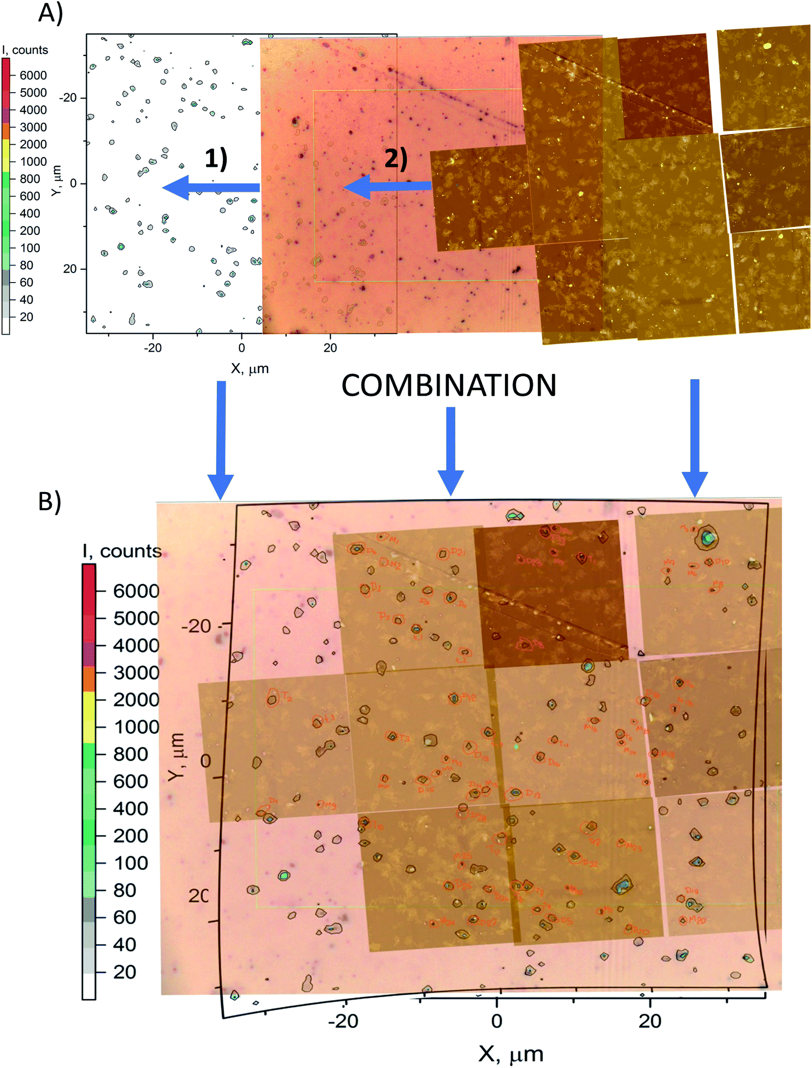 | ||
| Fig. 1 (A) Map combination process: (1) alignment of optical image on Raman map; (2) alignment of AFM maps on the combination of optical image and Raman map. (B) Result of the combination process. | ||
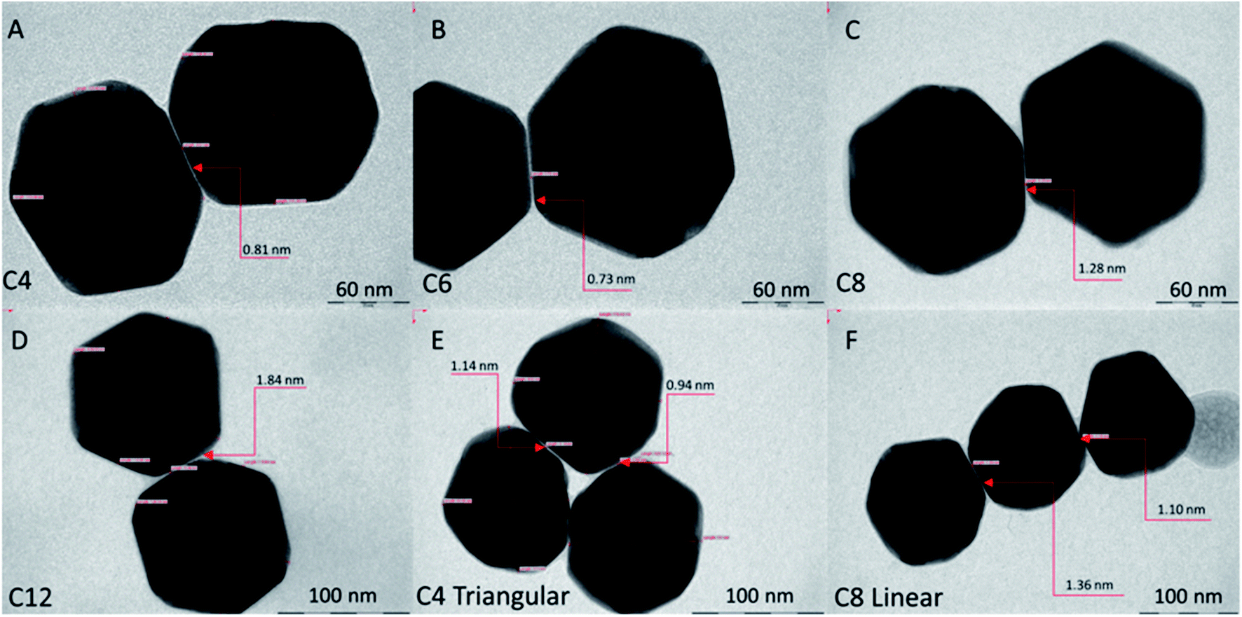 | ||
| Fig. 2 TEM images of AuNPs modified with mixed SAMs of 2-MOTP and mercaptocarboxylic acid. (A–D) Representative dimers of AuNPs. (E and F) Trimers in triangular and linear conformations. | ||
2. Large Raman maps and smaller AFM or SEM maps were transferred to the Adobe Photoshop image manipulation program.
3. The Raman map was made stationary in the program, and AFM or SEM maps were carefully aligned to the Raman map by decreasing their transparency and overlapping Raman signals to the nanoparticles in AFM and SEM maps (see Fig. 1).
4. In the case of AFM overlapping, ×100 microscope images were used to ensure topographical matching.
5. In the process of overlapping, the discrepancies in map orientations and proportions were compensated by slightly distorting the map images.
6. After alignment, each monomer, dimer, and trimer in the map overlap region was located and marked, as seen in Fig. 1A and B.
7. Then, every marked particle was identified in either AFM software or SEM software and underwent gap and surface area measurements.
8. Next, the Raman signal of each aligned particle was located by the OriginPro program and recorded.
9. Finally, standard data analysis and visualization were performed with spatial and Raman parameters known for each particle in the map region.
Results and discussion
Raman spectra and map combination analysis
All Raman spectra for maps were taken by using 633 nm laser excitation. Our previous study found that excitation with a 633 nm laser produces higher Raman intensity and subsequently higher signal-to-noise ratio than 532 nm laser excitation.61 This was explained by a superior electron–hole generation rate and an increase in the number of electrons and holes interacting with the gap mode upon 633 nm laser excitation.62 The measured Raman spectra for 2-MOTP Raman reporter on the surface of Au and Ag substrates can be seen in Fig. 3. Spectra of different substrates represent samples modified with different mercaptocarboxylic acids. By analyzing the representative 2-MOTP Raman peak between 1030 and 1045 cm−1, we can observe that an increase in mercapto chain length leads to a decrease in Raman intensity for monomers, dimers, and trimers. This is the direct effect of changes in nanoparticle–nanoparticle and nanoparticle-substrate gap distance. We can also see that Raman signal enhancement decreases with a reduction of agglomeration, which shows an emergence of “hot spots” in dimers and trimers.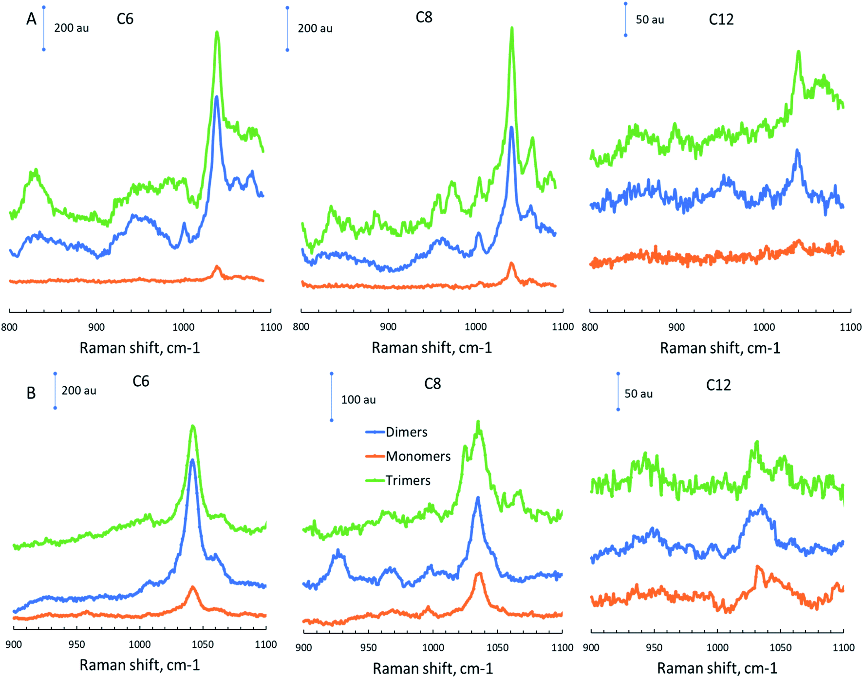 | ||
| Fig. 3 Raman spectra for AuNPs with different mercaptan chain lengths (C6, C8, C12) on (A) Au substrate and (B) Ag substrate. | ||
By using the map combination method, we were able to characterize 1224 nanoparticles according to their agglomeration, size and other spatial parameters, and Raman signal intensity. Of these 1224 nanoparticles, 533 are dimers, 648 are monomers, and 43 are trimers. Therefore, on average, the observed nanoparticle association process has produced 44% dimerization and only 4% trimerization.
However, we did not count nanoparticles in agglomerations higher than trimers, which suggests that the ratio of agglomerated nanoparticles to monomers is even higher. Ultimately, the use of this map combination technique provided us with an efficient way to quantify the large amount of numerical and visual data, which was used for subsequent data analysis. High-resolution examples of the combination can be seen in ESI Fig. S12–S31.†
Raman intensity comparison across four substrates
Hereafter, we report results from measurements on four different substrate materials for SERS: gold and silver films, the most common SERS substrate materials to be referenced, due to their widespread use; aluminum film and silicon wafer, which serve as alternatives for common plasmonic metal substrates. Results of our experiments using these substrates can be observed in Fig. 4–7 and ESI Tables S1–S5, S9.† These tables show that the nanoparticles, both monomers and dimers, show higher signals on the gold substrate. The measurements on silver film substrate were second in intensity, followed by measurements on aluminum film and silicon wafer. However, the order of magnitude of signal on gold and silver monomers is the same, and for C8, C12, and C16 monomers, the signal is, on average, about the same on both substrates. A similar slight advantage in SERS EF for ERLs (60 nm diameter AuNPs modified with antibodies and 4-nitrobenzenethiol) on gold film vs. SERS EF for the same ERLs on silver film was reported by Sergiienko et al. (EF 4.4 × 10⁵ on gold; EF 3.4 × 10⁵ on silver).61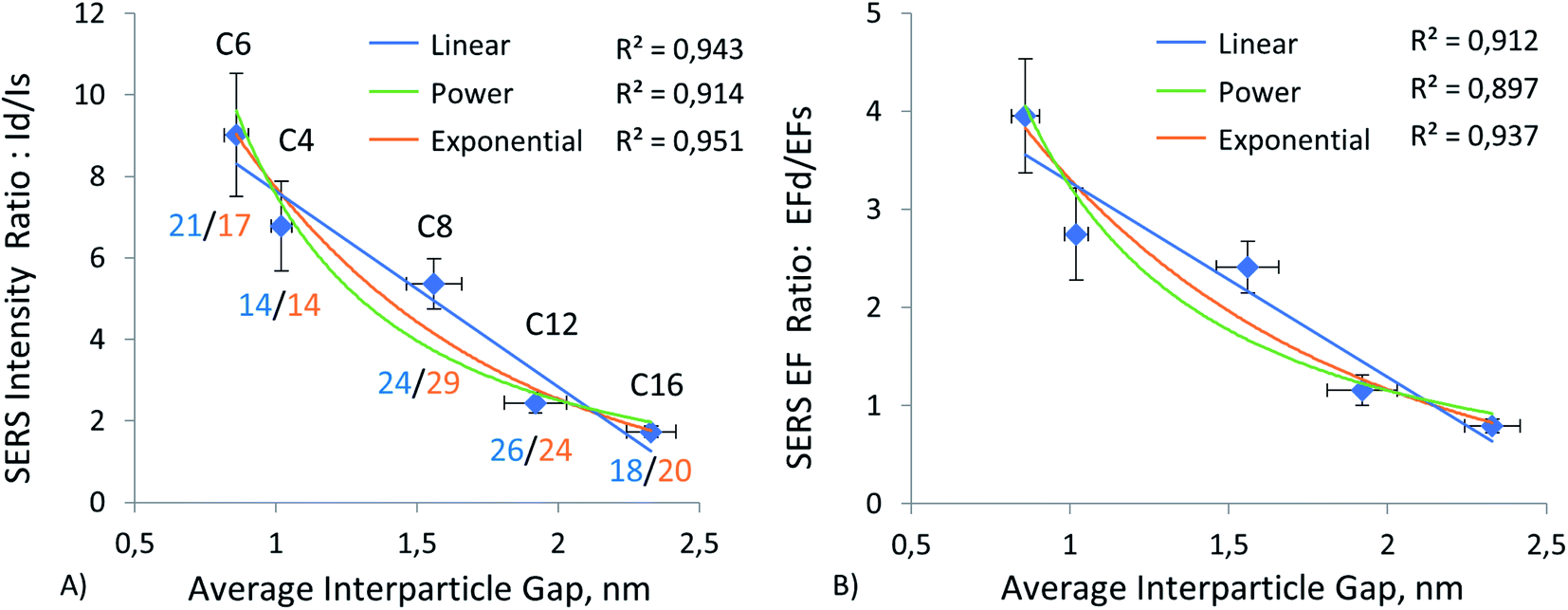 | ||
| Fig. 4 Data for dimers on Au surface. (A) Plot of SERS intensity against the average interparticle distance. (B) Plot of SERS EF ratio (EF dimer/EF single particle) vs. the average interparticle distance. Number of dimers/number of single particles is shown for each sample (blue, dimers; orange, single particles). | ||
 | ||
| Fig. 5 Data for dimers on Al surface. (A) Plot of SERS intensity against the average interparticle distance. (B) Plot of SERS EF ratio vs. the average interparticle distance. Sums of signal from two pixels with maximum intensity for each dimer or monomer were averaged. | ||
 | ||
| Fig. 6 Data for dimers on Si wafer surface. (A) Plot of SERS intensity against the average interparticle distance. (B) Plot of SERS EF ratio vs. the average interparticle distance. | ||
 | ||
| Fig. 7 Data for dimers on Ag surface and comparison of Id/Is ratios between 4 substrates. (A) Plot of SERS intensity ratios Id/Is against the average interparticle gap. (B) Plot of SERS intensity ratios Id/Is against the average interparticle gap for the four substrates. | ||
The advantages of a gold substrate can be explained by its unreactive nature, while both metals have a high electron density of 5.9 × 1022 cm−3 (5.86 × 1022 cm−3 for silver), and a lower onset for the interband transition (620 nm for gold and 310 nm for silver) than the excitation wavelength.63,64 The latter parameter determines the energy losses of the metal – the losses increase rapidly for excitation at frequencies higher than the onset for the interband transition. This increasing energy loss helps explain why SERS signals of nanoparticles on gold with 633 nm laser excitation were about 40 times higher than that of the same nanoparticles on gold with 532 nm laser excitation.61 Furthermore, the LSPR of gold nanoparticles for both monomers (λmax of about 570 nm) and dimers should be closer to the SPR resonant wavelength of a gold film rather than to the much lower SPR wavelength of silver film. For instance, Suzuki et al. observed a resonant wavelength of SPR sensors close to 635 nm, with a gold film thickness of about 80 nm, which would almost ideally match our excitation wavelength.65 Albeit, the maximum SPR wavelength reported for 10 nm silver film by Mohan et al. was about 498 nm.66
Beyond this LSPR/SPR mismatch of gold nanoparticles and substrate, which likely increases significantly from gold to silver, there is another factor that makes silver film an unfavorable choice for a SERS substrate, as compared to gold film. This is the potential oxidation of silver film during storage, preparation steps, and measurements. The growth of an oxide layer on a silver surface was shown to decrease SERS signal by 2.5 times, both theoretically and experimentally.67 Similarly, the aluminum film substrate has the highest electron density among the measured substrates (18.1 × 1022 cm−3).63 However, it typically has several nanometer thick layers of oxide on the surface,68 which should significantly decrease SERS signal intensity on this material. Finally, silicon semiconductors demonstrated the weakest plasmonic coupling of monomer gold nanoparticles to the substrate, resulting in the lowest signal among the four substrates, as expected.
The trend of decreasing intensity from gold and silver to aluminum and silicon observed for monomers is relevant for SERS sensing applications. For instance, it helps in understanding how substrate choice may impact the SERS signal of ERLs in SERS sandwich immunoassays.69 The trends for the ratio of intensities between dimers and monomers are visualized in Fig. 4–7. Here, we can observe the number of dimers and monomers in blue and yellow, respectively. According to these numbers, on average, our ratio of characterized dimers to monomers was close to 1. Since S/N ratios for both dimers and monomers were relatively low on silicon and we considered the majority but not all particles (taking only monomers and dimers with a Raman S/N level above 5), we cannot correctly compare the homogeneity of the signal on silicon to that on other substrates, where all particles were counted.
However, the three metallic substrates can be compared in terms of homogeneity. We found that dimers on gold film are more homogenous in terms of Raman signal than those on silver and aluminum films. 20% of dimers on gold are responsible for 35% of the total signal, and the same share of dimers on silver and aluminum produced 54% and 69% of the signal, respectively. This trend is also observed for monomers, where silver was found to be less homogenous than aluminum and gold, with 45%, 37%, and 32% of the signal produced by 20% of monomers, respectively.
The variability of the signal could at least partially be attributed to the surface roughness of metal films, which may have a significant effect on Raman signal.70–72 The average surface roughness of all four substrates as measured by AFM was about 3–4 nm; the gold film had a slightly lower roughness of about 2.8 nm while Si, Ag, and Al had a roughness in the range of 3.2–3.9 nm.61 It is likely that the major contribution to this difference may come from the possible variation in oxide layer thickness, which would create fluctuations in the plasmonic coupling between gold nanoparticles and each substrate. Since gold is expected to have a negligible oxide layer relative to Al (at least 5–10 nm thick Al2O3 layer), the effect of the oxide layer on gold is expected to be the lowest.67,73
As for the deviation in the ratio of EFs for dimers to EF of monomers, or in other words, the relative EF of dimers, we observed the highest standard deviation and the highest error bar for the C4 sample on Al film. When maximum intensity in one pixel was averaged in the same way as intensities, EF ratios were calculated for all substrates (Fig. S11†). Hence, we decided to use the sum of two maximum signals instead of the maximum signal for calculations for samples on Al film. The two-pixel approach that we applied only for samples on Al film decreased Id/Im and EFd/EFm ratios, as shown in Fig. 5 (vs. Fig. S11†). On the other hand, it decreased standard deviations and error bars for Al film samples. The silicon wafer as a substrate, calculated similarly to other substrates by the maximum intensity in one point/pixel, has the second-highest standard error for relative EF of dimers for a gap of about 0.8–0.9 nm, as shown in Fig. 7B. In this case, by far most of the signal originates from hot spots between nanoparticles, and the signal is sensitive to minor variations in gap distance and variations in the nanoparticle shape.61 The relative standard deviation of the interparticle gap for the C6 sample measured by TEM was 20%. Therefore, this relatively high error in the average EF ratio is justified. On average, gold and silver showed slightly more uniform Raman signal ratios than aluminum. Presumably, those classic plasmonic metal substrates were less affected by the oxide layer formed on the metal surface than Al film.
Nonetheless, the agglomeration of nanoparticles increases the standard deviation of signal relative to that of single nanoparticles. Thus, overall, the nanoparticle–nanoparticle gap distance significantly impacts the total SERS signal intensity, which is our next topic of discussion.
Gap distance dependence across four substrates
To investigate the effect of gap distance variation in dimers, we modified ERLs with mercaptan acids of different chain lengths. This technique helped us to control the gap distance and to achieve sub-nanometer separation. As mentioned in the methods, we measured the gap distance by using TEM images. The detailed procedure for this measurement is available in our previous publication.61 Results of this measurement can be seen in ESI (Table S7 and graph S8†). These results showed a linear increase in gap distance from C4 to C16, with C6 being a special case. Because it is in cyclic form, the gap distance is even smaller despite the increase in carbon number. Moreover, by using this high linearity between gap distance and mercaptan chain length, we were able to extrapolate the gap distance for C3 mercaptan acid, which was used for particles on the silver surface when our stock of C4 mercaptan acid was depleted, and we used C3 instead of C4 or C6 as short-chain thiol in the experiment using silver film. The results of this gap distance investigation can be observed in Fig. 4–7 and ESI Tables S1–S4.†Fig. 4A, 5A, 6A, and 7A represent a relationship between relative Raman intensity of dimers and gap distance variation, where the relative Raman intensity of dimers is represented by the ratio of dimer intensity to monomer intensity. Overall, generalizing the trends observed for the four different substrates, we can see that the relative SERS intensity of dimers decreases upon an increase in the gap between nanoparticles. The steepest negative slope is observed for gold film and silicon wafer substrates, which is partially in line with the observation of a higher relative SERS EF for 60 nm diameter AuNP dimers on silicon than for 60 nm diameter AuNP dimers on other substrates (Au, Ag), as reported by Sergiienko et al.61 The maximum ratio of the dimer to monomer EFs is about 4.3 and this ratio is in general agreement with the polarization-controlled SERS study performed by the Xia group, of an unspecified number of silver monomers and silver dimers, both encapsulated in SiO2 on the surface of silicon. In that study, the authors reported 1.5 to 17 times (the geometric average of 1.5 and 17 is 5) higher EFs for dimers than for monomers of the same sphere diameter, 80 nm, upon transverse and longitudinal polarization of exciting light, respectively.35
This trend can be observed more clearly in Fig. 7B, where results for all four substrates are positioned next to each other. The figure shows that the trend goes from gold and silicon to silver and aluminum in decreasing order. The same conclusion can be drawn by observing enhancement factor ratios between dimers and monomers for all four substrates in Fig. 4B, 5B, 6B. The trend is identical to the trend for the ratio of intensities. Moreover, we can see that a minor change in gap distance can significantly affect both the intensity and enhancement factor in all cases. For example, the decrease of 0.5 nm for the gold film going from C8 to C6 can almost double the intensity and EF, similarly to when going from C12 to C8. However, these drastic changes are less prominent for the other substrates, as the overall signal enhancement decreases because of previously mentioned factors, like surface homogeneity and oxide formation, electronic properties, etc. In addition, despite significant differences between these substrates, the Raman intensity ratios start to converge when the gap distance goes beyond 2 nm. This implies that the substrate effect becomes less and less important with an increase in the dimer gap distance. However, we need to discuss the trend of relative (I dimer/I monomer) Raman intensity against gap distance in more detail, as it varies from substrate to substrate and can help in choosing optimal gap distances for specific applications.
The relationship between gap distance in dimers and Raman signal enhancement is still a topic for discussion. According to the works of the Van Duyne group, this relationship follows a power function, when a simplified sphere model and E4 approximation are used.19,74 The group of Van Duyne showed that we should account for both long-range and short-range SERS effects, as it provides a better fit for experimental data.74 However, Kessentini et al. showed that the relationship of SERS enhancement to gap distance could exhibit inverse exponential dependence for gold dimer nanoantennae with slanted gaps.75 This behavior was explained by the exponential decay of LSPR demonstrated by several studies.76–78 Hence, we found that the trend may also depend on the substrate, after measuring more than a thousand dimers and monomers. Our results comparing three trends (linear, power, and exponential) can be observed in Fig. 4–8 and ESI Table S9.† We can observe that exponential fitting is more suitable for gold film and silicon wafer, as it gives 1 − R2 values that are almost two times higher than those of power and linear fits. Contrarily, in the case of the aluminum film, we see that adherence to a power function is better than to exponential and linear fits. As for the silver film, both fits exhibit similar performance.
 | ||
| Fig. 8 Data for trimers on Al and Au surfaces. (A) Plot of SERS intensity ratio against the number of carbon atoms in mercaptocarboxylic acid on aluminium. (B) Plot of SERS intensity ratio against the number of carbon atoms in mercaptocarboxylic acid on gold. | ||
Trimers on Au and Al substrates
We were able to measure and analyze the SERS signal for a selection of trimers of AuNPs on two substrates, Au and Al, but those numbers (∼50 trimers) were about ten-fold smaller than the number of dimers analyzed from the same maps (478), since trimers were far less common than dimers on every substrate. The results of Raman measurement for the Al substrate can be observed in Fig. 8A.Again, even for averages of a much smaller number of data points, inverse exponential relationships prevail over an inverse linear relationship, as demonstrated by corresponding R2 values. Thus, the intensity of the Raman signal decreases with an increase in the interparticle gap, as for dimers. Another trend in Fig. 8A is an increase in the It/Is ratio variance with a decrease in the interparticle gap on the Al surface. The results presented in Fig. 8 are only for the linear configuration of trimers, since only a few triangular trimers were observed on the surface of aluminum. Nevertheless, we can assume from those results that due to their relative rarity, the formation of trimers has a significantly lower impact on the overall enhancement of Raman signal than does dimerization.
Summary and conclusions
What we found during this study is that even a slight change in interparticle distance can cause a significant difference in the relative signal intensity of dimers vs. single AuNPs. For instance, a ∼16% decrease in the interparticle gap boosted EF dimer/EF single particle ratio by 50%, from 2.7 to 4.0. We also found that the gold film substrate creates a more reproducible SERS signal from AuNP dimers than silver film or Al film, which has the broadest distribution of SERS intensity among dimers. This is because trimers are much less common than dimers, and we obtained enough data only for AuNPs on Au and Al substrates. Trimers on both substrates showed the same inverse exponential trend as the trend for dimers. However, the extra enhancement of signal in SERS assays (sandwich immunoassays, etc.) is mainly caused by dimer AuNPs, and the obtained data can help predict at what interparticle distance this extra enhancement due to AuNP association in the assay can be minimized. For instance, for gold substrate and 100 nm AuNPs, this gap distance would be about 2.0–2.2 nm (between C12 and C16, when EF dimer/EF single particle ∼1.0). Since EF dimer/EF single particle converges at a gap distance above 2 nm for all four of the studied substrates, we can conclude that the effect of dimerization becomes muted at those distances, regardless of the substrate nature.This paper demonstrated the effect of interparticle gap variation on the relative SERS signal enhancement on four different substrates. Dimers on all substrates exhibited an inverse exponential trend for the intensity and SERS EF ratios versus the interparticle distance increase. This gave us insight into the impact of nanoparticle agglomeration/association on SERS signal in several analytical techniques, such as sandwich immuno- or apto-assays, etc. Furthermore, it was found that an increase in the interparticle gap of more than 2 nm can even lead to a decrease in enhancement factors, compared to single particles/monomers, particularly for assays on Al film (EFd/EFs = 0.7 for C16). On the contrary, a decrease in the interparticle gap from 2.3 to 1.0–0.9 nm leads to a 4–5 times increase in intensity (1.7 to 9) and enhancement (0.8 to 4), compared to single monomers on a gold film substrate. These numbers are lower for the remaining three substrates, but the trend remains the same. Overall, we still observe significant individual variations within the SERS signal of most of the samples on every substrate, particularly for small ∼1 nm average interparticle gaps, as predicted in the literature.32 However, there are still clear trends of average SERS enhancement of dimers and trimers vs. enhancement of single nanoparticles as a function of the interparticle gap, even with non-ideally spherical commercial gold nanoparticles, labeled with SERS markers and measured on plasmonic substrates. Those average substrate-dependent trends are revealed in this paper and may help in the selection/prediction of optimal interparticle distance and selection of optimal substrate for specific analytical or other applications.
A novel method for the combination of optical-Raman-AFM or Raman-SEM maps was introduced, where increasing the transparency of overlaid images is used for a robust combination of 3 maps into 1 map. This method can decrease time, effort, and the minimum required qualification of personnel (they no longer have to be an efficient post-doc). It can also make single-particle characterization, realized by combining two or three nano- or microimaging techniques, far more affordable and commonly practiced in research. Those combinations still require plenty of imaging time (including overnight Raman maps), but they are becoming a more widespread and affordable procedure. In total, we have quantified signals from 1224 nanoantennae (533 dimers, 648 single particles, and 43 trimers), using 31 Raman, 81 AFM, and 66 SEM maps/images. For comparison, in a highly cited paper of the Van Duyne group (about 660+ citations to date), TEM, LSPR, and SERS measurements were performed only on 67 individual nanoantennae on a single substrate (TEM grid).32 Moreover, seminal work by Chen et al., showcasing the effect of NP agglomeration on Raman signal, used 20 nm Au@Ag core–shell NPs with a uniform average gap distance of 0.8 nm and the Raman spectra were collected from the sample solution.79 Albeit, our methodology more closely replicates the possible real-life applications of analyte detection through SERS by finding a structure–activity relationship on four different substrates, including most commonly used gold and silver films and commercially available AuNPs.
Overall, we can suggest that the controlled agglomeration of nanoparticles can be beneficial for SERS and likely for other surface-enhanced spectroscopic methods used for the detection of trace amounts of analyte, where the relative increase in signal variability can be compensated by an increase in S/N ratio due to higher enhancement. Finally, the novel combination method between Raman, optical, AFM, or SEM maps can help analyze the spectral properties vs. morphology data more efficiently. It may open a new chapter in the study of the structure–activity relationship for surface spectroscopies in situ.
Author contributions
Alexandr Arbuz contributed to development of the 3 to 1 map combination method, which might be the most creative contribution, but also he did all SEM measurements and some Raman microscope measurements and data analysis. Alisher Sultangaziyev contributed to some Raman microscope measurements and data analysis, and he contributed to making figures and tables as well as to writing the draft of the paper and part of the response to reviewers. Alisher Rapikov and Zhanar Kunushpayeva contributed to sample preparation, Raman microscope measurements and data analysis. Rostislav Bukasov provided funding and idea/plan of the research, contributing to writing of the paper and response to reviewers, and coordination of efforts of all authors.Conflicts of interest
Authors are unaware of any conflict of interest related to this paper.Acknowledgements
This research is supported by the Nazarbayev University Faculty Development Competitive Research grant SST2018045 “Fundamental and applied SERS for detection of cancer biomarkers” (FASERSDCB).Notes and references
- D. L. Jeanmaire and R. P. Van Duyne, Surface Raman spectroelectrochemistry Part I. Heterocyclic, aromatic, and aliphatic amines adsorbed on the anodized silver electrode, J. Electroanal. Chem., 1977, 84(1), 1–20 CrossRef CAS.
- M. G. Albrecht and J. A. Creighton, Anomalously intense Raman spectra of pyridine at a silver electrode, J. Am. Chem. Soc., 1977, 99(15), 5215–5217 CrossRef CAS.
- B. Sharma, R. R. Frontiera, A. I. Henry, E. Ringe and R. P. Van Duyne, SERS: Materials, applications, and the future, Mater. Today, 2012, 15(1–2), 16–25 CrossRef CAS.
- G. Wang, H.-Y. Park, R. J. Lipert and M. D. Porter, Mixed Monolayers on Gold Nanoparticle Labels for Multiplexed Surface-Enhanced Raman Scattering Based Immunoassays, Anal. Chem., 2009, 81(23), 9643–9650 CrossRef CAS PubMed.
- S. Schlucker, Surface-Enhanced Raman Spectroscopy: Concepts and Chemical Applications, Angew. Chem., Int. Ed., 2014, 53(19), 4756–4795 CrossRef PubMed.
- D. Radziuk and H. Moehwald, Prospects for plasmonic hot spots in single molecule SERS towards the chemical imaging of live cells, Phys. Chem. Chem. Phys., 2015, 17(33), 21072–21093 RSC.
- A. J. Driscoll, M. H. Harpster and P. A. Johnson, The development of surface-enhanced Raman scattering as a detection modality for portable in vitro diagnostics: progress and challenges, Phys. Chem. Chem. Phys., 2013, 15(47), 20415–20433 RSC.
- Z. Guo, Y. Jia, X. Song, J. Lu, X. Lu, B. Liu, J. Han, Y. Huang, J. Zhang and T. Chen, Giant Gold Nanowire Vesicle-Based Colorimetric and SERS Dual-Mode Immunosensor for Ultrasensitive Detection of Vibrio parahemolyticus, Anal. Chem., 2018, 90(10), 6124–6130 CrossRef CAS PubMed.
- J. B. Song, P. Huang, H. W. Duan and X. Y. Chen, Plasmonic Vesicles of Amphiphilic Nanocrystals: Optically Active Multifunctional Platform for Cancer Diagnosis and Therapy, Acc. Chem. Res., 2015, 48(9), 2506–2515 CrossRef CAS PubMed.
- L. A. Lane, X. M. Qian and S. M. Nie, SERS Nanoparticles in Medicine: From Label-Free Detection to Spectroscopic Tagging, Chem. Rev., 2015, 115(19), 10489–10529 CrossRef CAS.
- D. S. Grubisha, R. J. Lipert, H. Y. Park, J. Driskell and M. D. Porter, Femtomolar detection of prostate-specific antigen: An immunoassay based on surface-enhanced Raman scattering and immunogold labels, Anal. Chem., 2003, 75(21), 5936–5943 CrossRef CAS PubMed.
- R. A. Halvorson and P. J. Vikesland, Surface-Enhanced Raman Spectroscopy (SERS) for Environmental Analyses, Environ. Sci. Technol., 2010, 44(20), 7749–7755 CrossRef CAS PubMed.
- S. Nie and S. R. Emory, Probing Single Molecules and Single Nanoparticles by Surface-Enhanced Raman Scattering, Science, 1997, 275(5303), 1102–1106 CrossRef CAS PubMed.
- K. Kneipp, Y. Wang, H. Kneipp, L. T. Perelman, I. Itzkan, R. R. Dasari and M. S. Feld, Single molecule detection using surface-enhanced raman scattering (SERS), Phys. Rev. Lett., 1997, 78(9), 1667–1670 CrossRef CAS.
- J. P. Camden, J. A. Dieringer, Y. Wang, D. J. Masiello, L. D. Marks, G. C. Schatz and R. P. Van Duyne, Probing the structure of single-molecule surface-enhanced Raman scattering hot spots, J. Am. Chem. Soc., 2008, 130(38), 12616–12617 CrossRef CAS PubMed.
- R. Zhang, Y. Zhang, Z. C. Dong, S. Jiang, C. Zhang, L. G. Chen, L. Zhang, Y. Liao, J. Aizpurua, Y. Luo, J. L. Yang and J. G. Hou, Chemical mapping of a single molecule by plasmon-enhanced Raman scattering, Nature, 2013, 498(7452), 82–86 CrossRef CAS PubMed.
- R. Reverberi and L. Reverberi, Factors affecting the antigen-antibody reaction, Blood Transfus., 2007, 5(4), 227–240 Search PubMed.
- E. Hutter and J. H. Fendler, Exploitation of localized surface plasmon resonance, Adv. Mater., 2004, 16(19), 1685–1706 CrossRef CAS.
- P. L. Stiles, J. A. Dieringer, N. C. Shah and R. R. Van Duyne, Surface-Enhanced Raman Spectroscopy, Annu. Rev. Anal. Chem., 2008, 1, 601–626 CrossRef CAS PubMed.
- H. T. Phan and A. J. Haes, What Does Nanoparticle Stability Mean?, J. Phys. Chem. C, 2019, 123(27), 16495–16507 CrossRef CAS PubMed.
- L. Guerrini and D. Graham, Molecularly-mediated assemblies of plasmonic nanoparticles for Surface-Enhanced Raman Spectroscopy applications, Chem. Soc. Rev., 2012, 41(21), 7085–7107 RSC.
- T. Ishida, S. Tsuneda, N. Nishida, M. Hara, H. Sasabe and W. Knoll, Surface-Conditioning Effect of Gold Substrates on Octadecanethiol Self-Assembled Monolayer Growth, Langmuir, 1997, 13(17), 4638–4643 CrossRef CAS.
- A. Matikainen, T. Nuutinen, T. Itkonen, S. Heinilehto, J. Puustinen, J. Hiltunen, J. Lappalainen, P. Karioja and P. Vahimaa, Atmospheric oxidation and carbon contamination of silver and its effect on surface-enhanced Raman spectroscopy (SERS), Sci. Rep., 2016, 6, 37192 CrossRef CAS.
- M. W. Knight, N. S. King, L. Liu, H. O. Everitt, P. Nordlander and N. J. Halas, Aluminum for Plasmonics, ACS Nano, 2014, 8(1), 834–840 CrossRef CAS.
- K. Gudun, Z. Elemessova, L. Khamkhash, E. Ralchenko and R. Bukasov, Commercial Gold Nanoparticles on Untreated Aluminum Foil: Versatile, Sensitive, and Cost-Effective SERS Substrate, J. Nanomater., 2017, 2017, 8 Search PubMed.
- Z. Mukanova, K. Gudun, Z. Elemessova, L. Khamkhash, E. Ralchenko and R. Bukasov, Detection of Paracetamol in Water and Urea in Artificial Urine with Gold Nanoparticle@Al Foil Cost-efficient SERS Substrate, Anal. Sci., 2018, 34(2), 183–187 CrossRef CAS PubMed.
- K. B. Mogensen, M. Gühlke, J. Kneipp, S. Kadkhodazadeh, J. B. Wagner, M. Espina Palanco, H. Kneipp and K. Kneipp, Surface-enhanced Raman scattering on aluminum using near infrared and visible excitation, Chem. Commun., 2014, 50(28), 3744–3746 RSC.
- Z. Jiang, J. Xiangxu, S. Su, X. Wei, S. Lee and Y. He, Silicon-based reproducible and active surface-enhanced Raman scattering substrate for sensitive, specific and multiplex DNA detection, Appl. Phys. Lett., 2012, 100, 203104 CrossRef.
- M. Kosović, M. Balarin, M. Ivanda, V. Đerek, M. Marciuš, M. Ristić and O. Gamulin, Porous Silicon Covered with Silver Nanoparticles as Surface-Enhanced Raman Scattering (SERS) Substrate for Ultra-Low Concentration Detection, Appl. Spectrosc., 2015, 69, 1417–1424 CrossRef PubMed.
- G. Upender, R. Sathyavathi, B. Raju, C. Bansal and D. Narayana Rao, SERS study of molecules on Ag nanocluster films deposited on glass and silicon substrates by cluster deposition method, J. Mol. Struct., 2012, 1012, 56–61 CrossRef CAS.
- P. P. Edwards, A. Porch, M. O. Jones, D. V. Morgan and R. M. Perks, Basic materials physics of transparent conducting oxides, Dalton Trans., 2004, 19, 2995–3002 RSC.
- K. L. Wustholz, A. I. Henry, J. M. McMahon, R. G. Freeman, N. Valley, M. E. Piotti, M. J. Natan, G. C. Schatz and R. P. Van Duyne, Structure-Activity Relationships in Gold Nanoparticle Dimers and Trimers for Surface-Enhanced Raman Spectroscopy, J. Am. Chem. Soc., 2010, 132(31), 10903–10910 CrossRef CAS PubMed.
- S. L. Kleinman, R. R. Frontiera, A. I. Henry, J. A. Dieringer and R. P. Van Duyne, Creating, characterizing, and controlling chemistry with SERS hot spots, Phys. Chem. Chem. Phys., 2013, 15(1), 21–36 RSC.
- K. A. Willets, Super-resolution imaging of SERS hot spots, Chem. Soc. Rev., 2014, 43(11), 3854–3864 RSC.
- W. Li, P. H. Camargo, L. Au, Q. Zhang, M. Rycenga and Y. Xia, Etching and dimerization: a simple and versatile route to dimers of silver nanospheres with a range of sizes, Angew. Chem., Int. Ed. Engl., 2010, 49(1), 164–168 CrossRef CAS PubMed.
- K. J. Savage, M. M. Hawkeye, R. Esteban, A. G. Borisov, J. Aizpurua and J. J. Baumberg, Revealing the quantum regime in tunnelling plasmonics, Nature, 2012, 491(7425), 574–577 CrossRef CAS PubMed.
- S. F. Tan, L. Wu, J. K. W. Yang, P. Bai, M. Bosman and C. A. Nijhuis, Quantum Plasmon Resonances Controlled by Molecular Tunnel Junctions, Science, 2014, 343(6178), 1496 CrossRef CAS PubMed.
- M. S. Tame, K. R. McEnery, Ş. K. Özdemir, J. Lee, S. A. Maier and M. S. Kim, Quantum plasmonics, Nat. Phys., 2013, 9(6), 329–340 Search PubMed.
- J. A. Scholl, A. García-Etxarri, A. L. Koh and J. A. Dionne, Observation of quantum tunneling between two plasmonic nanoparticles, Nano Lett., 2013, 13(2), 564–569 CrossRef CAS.
- L. Mao, Z. Li, B. Wu and H. Xu, Effects of quantum tunneling in metal nanogap on surface-enhanced Raman scattering, Appl. Phys. Lett., 2009, 94(24), 243102 CrossRef.
- W. Zhu, R. Esteban, A. G. Borisov, J. J. Baumberg, P. Nordlander, H. J. Lezec, J. Aizpurua and K. B. Crozier, Quantum mechanical effects in plasmonic structures with subnanometre gaps, Nat. Commun., 2016, 7, 11495 CrossRef CAS PubMed.
- K. D. Alexander, M. J. Hampton, S. Zhang, A. Dhawan, H. Xu and R. Lopez, A high-throughput method for controlled hot-spot fabrication in SERS-active gold nanoparticle dimer arrays, J. Raman Spectrosc., 2009, 40(12), 2171–2175 CrossRef CAS.
- C. Tserkezis, R. W. Taylor, J. Beitner, R. Esteban, J. J. Baumberg and J. Aizpurua, Optical Response of Metallic Nanoparticle Heteroaggregates with Subnanometric Gaps, Part. Part. Syst. Charact., 2014, 31(1), 152–160 CrossRef CAS.
- H. W. Cheng, Z. Skeete, Q. M. Ngo, J. Luo and C. J. Zhong, Harnessing the interparticle J-aggregate induced plasmonic coupling for surface-enhanced Raman scattering, Phys. Chem. Chem. Phys., 2015, 17(43), 28529–28533 RSC.
- D. Steinigeweg, M. Schuetz and S. Schluecker, Single gold trimers and 3D superstructures exhibit a polarization-independent SERS response, Nanoscale, 2013, 5(1), 110–113 RSC.
- Q. Hao, H. Huang, X. Fan, Y. Yin, J. Wang, W. Li, T. Qiu, L. Ma, P. K. Chu and O. G. Schmidt, Controlled Patterning of Plasmonic Dimers by Using an Ultrathin Nanoporous Alumina Membrane as a Shadow Mask, ACS Appl. Mater. Interfaces, 2017, 9(41), 36199–36205 CrossRef CAS PubMed.
- A. Hakonen, M. Svedendahl, R. Ogier, Z. J. Yang, K. Lodewijks, R. Verre, T. Shegai, P. O. Andersson and M. Kall, Dimer-on-mirror SERS substrates with attogram sensitivity fabricated by colloidal lithography, Nanoscale, 2015, 7(21), 9405–9410 RSC.
- T. Atay, J. H. Song and A. V. Nurmikko, Strongly interacting plasmon nanoparticle pairs: From dipole-dipole interaction to conductively coupled regime, Nano Lett., 2004, 4(9), 1627–1631 CrossRef CAS.
- S. Fateixa, H. I. S. Nogueira and T. Trindade, Hybrid nanostructures for SERS: materials development and chemical detection, Phys. Chem. Chem. Phys., 2015, 17(33), 21046–21071 RSC.
- S. Simoncelli, Y. Li, E. Cortés and S. A. Maier, Nanoscale Control of Molecular Self-Assembly Induced by Plasmonic Hot-Electron Dynamics, ACS Nano, 2018, 12(3), 2184–2192 CrossRef CAS PubMed.
- L. Song, Y. Huang, Z. Nie and T. Chen, Macroscopic two-dimensional monolayer films of gold nanoparticles: fabrication strategies, surface engineering and functional applications, Nanoscale, 2020, 12(14), 7433–7460 RSC.
- X. Lu, Y. Huang, B. Liu, L. Zhang, L. Song, J. Zhang, A. Zhang and T. Chen, Light-Controlled Shrinkage of Large-Area Gold Nanoparticle Monolayer Film for Tunable SERS Activity, Chem. Mater., 2018, 30(6), 1989–1997 CrossRef CAS.
- R. T. Hill, K. M. Kozek, A. Hucknall, D. R. Smith and A. Chilkoti, Nanoparticle-Film Plasmon Ruler Interrogated with Transmission Visible Spectroscopy, ACS Photonics, 2014, 1(10), 974–984 CrossRef CAS PubMed.
- J. H. Yoon, F. Selbach, L. Langolf and S. Schlücker, Ideal Dimers of Gold Nanospheres for Precision Plasmonics: Synthesis and Characterization at the Single-Particle Level for Identification of Higher Order Modes, Small, 2018, 14(4), 1702754 CrossRef PubMed.
- J. H. Yoon, F. Selbach, L. Schumacher, J. Jose and S. Schlücker, Surface Plasmon Coupling in Dimers of Gold Nanoparticles: Experiment and Theory for Ideal (Spherical) and Nonideal (Faceted) Building Blocks, ACS Photonics, 2019, 6(3), 642–648 CrossRef CAS.
- A. Kamińska, K. Winkler, A. Kowalska, E. Witkowska, T. Szymborski, A. Janeczek and J. Waluk, SERS-based Immunoassay in a Microfluidic System for the Multiplexed Recognition of Interleukins from Blood Plasma: Towards Picogram Detection, Sci. Rep., 2017, 7(1), 10656 CrossRef PubMed.
- S. M. Stranahan, E. J. Titus and K. A. Willets, Discriminating Nanoparticle Dimers from Higher Order Aggregates through Wavelength-Dependent SERS Orientational Imaging, ACS Nano, 2012, 6(2), 1806–1813 CrossRef CAS PubMed.
- C. H. van Hoorn, C. Wessels, F. Ariese and A. J. G. Mank, Fast High-Resolution Screening Method for Reactive Surfaces by Combining Atomic Force Microscopy and Surface-Enhanced Raman Scattering, Appl. Spectrosc., 2017, 71(7), 1551–1559 CrossRef CAS PubMed.
- C. S. Sweetenham, M. Larraona-Puy and I. Notingher, Simultaneous Surface-Enhanced Raman Spectroscopy (SERS) and Atomic Force Microscopy (AFM) for Label-Free Physicochemical Analysis of Lipid Bilayers, Appl. Spectrosc., 2011, 65(12), 1387–1392 CrossRef CAS.
- V. Prokopec, J. Cejkova, P. Matějka and P. Hasal, Preparation of SERS-active substrates with large surface area for Raman spectral mapping and testing of their surface nanostructure, Surf. Interface Anal., 2008, 40(3-4), 601–607 CrossRef CAS.
- S. Sergiienko, K. Moor, K. Gudun, Z. Yelemessova and R. Bukasov, Nanoparticle-nanoparticle vs. nanoparticle-substrate hot spot contributions to the SERS signal: studying Raman labelled monomers, dimers and trimers, Phys. Chem. Chem. Phys., 2017, 19(6), 4478–4487 RSC.
- C. Lumdee, B. Yun and P. G. Kik, Gap-Plasmon Enhanced Gold Nanoparticle Photoluminescence, ACS Photonics, 2014, 1(11), 1224–1230 CrossRef CAS.
- V. Palenskis, Drift Mobility, Diffusion Coefficient of Randomly Moving Charge Carriers in Metals and Other Materials with Degenerated Electron Gas, World J. Condens. Matter Phys., 2013, 3, 73–81 CrossRef CAS.
- E. Cottancin, G. Celep, J. Lermé, M. Pellarin, J. R. Huntzinger, J. L. Vialle and M. Broyer, Optical Properties of Noble Metal Clusters as a Function of the Size: Comparison between Experiments and a Semi-Quantal Theory, Theor. Chem. Acc., 2006, 116(4), 514–523 Search PubMed.
- H. Suzuki, M. Sugimoto, Y. Matsui and J. Kondoh, Effects of gold film thickness on spectrum profile and sensitivity of a multimode-optical-fiber SPR sensor, Sens. Actuators, B, 2008, 132(1), 26–33 CrossRef CAS.
- D. Bharathi Mohan, K. Sreejith and C. S. Sunandana, Surface plasmon–exciton transition in ultra-thin silver and silver iodide films, Appl. Phys. B: Lasers Opt., 2007, 89(1), 59–63 CrossRef CAS.
- N. Michieli, R. Pilot, V. Russo, C. Scian, F. Todescato, R. Signorini, S. Agnoli, T. Cesca, R. Bozio and G. Mattei, Oxidation effects on the SERS response of silver nanoprism arrays, RSC Adv., 2017, 7(1), 369–378 RSC.
- T. Campbell, R. K. Kalia, A. Nakano, P. Vashishta, S. Ogata and S. Rodgers, Dynamics of Oxidation of Aluminum Nanoclusters using Variable Charge Molecular-Dynamics Simulations on Parallel Computers, Phys. Rev. Lett., 1999, 82(24), 4866–4869 CrossRef CAS.
- Z. Kunushpayeva, A. Rapikov, A. Akhmetova, A. Sultangaziyev, D. Dossym and R. Bukasov, Sandwich SERS immunoassay of human immunoglobulin on silicon wafer compared to traditional SERS substrate, gold film, Sensing and Bio-Sensing Research, 2020, 29, 100355 CrossRef.
- C. Lee, C. S. Robertson, A. H. Nguyen, M. Kahraman and S. Wachsmann-Hogiu, Thickness of a metallic film, in addition to its roughness, plays a significant role in SERS activity, Sci. Rep., 2015, 5(1), 11644 CrossRef CAS PubMed.
- A. Trügler, J.-C. Tinguely, G. Jakopic, U. Hohenester, J. R. Krenn and A. Hohenau, Near-field and SERS enhancement from rough plasmonic nanoparticles, Phys. Rev. B, 2014, 89(16), 165409 CrossRef.
- Y. Zhao, X. Liu, D. Y. Lei and Y. Chai, Effects of surface roughness of Ag thin films on surface-enhanced Raman spectroscopy of graphene: spatial nonlocality and physisorption strain, Nanoscale, 2014, 6(3), 1311–1317 RSC.
- M. Erol, Y. Han, S. K. Stanley, C. M. Stafford, H. Du and S. Sukhishvili, SERS Not To Be Taken for Granted in the Presence of Oxygen, J. Am. Chem. Soc., 2009, 131(22), 7480–7481 CrossRef CAS PubMed.
- S. S. Masango, R. A. Hackler, N. Large, A.-I. Henry, M. O. McAnally, G. C. Schatz, P. C. Stair and R. P. Van Duyne, High-Resolution Distance Dependence Study of Surface-Enhanced Raman Scattering Enabled by Atomic Layer Deposition, Nano Lett., 2016, 16(7), 4251–4259 CrossRef CAS PubMed.
- S. Kessentini, D. Barchiesi, C. D'Andrea, A. Toma, N. Guillot, E. Di Fabrizio, B. Fazio, O. M. Maragó, P. G. Gucciardi and M. Lamy de la Chapelle, Gold Dimer Nanoantenna with Slanted Gap for Tunable LSPR and Improved SERS, J. Phys. Chem. C, 2014, 118(6), 3209–3219 CrossRef CAS.
- S. S. Aćimović, M. P. Kreuzer, M. U. González and R. Quidant, Plasmon Near-Field Coupling in Metal Dimers as a Step toward Single-Molecule Sensing, ACS Nano, 2009, 3(5), 1231–1237 CrossRef PubMed.
- A. M. Funston, C. Novo, T. J. Davis and P. Mulvaney, Plasmon Coupling of Gold Nanorods at Short Distances and in Different Geometries, Nano Lett., 2009, 9(4), 1651–1658 CrossRef CAS PubMed.
- P. K. Jain, W. Huang and M. A. El-Sayed, On the Universal Scaling Behavior of the Distance Decay of Plasmon Coupling in Metal Nanoparticle Pairs: A Plasmon Ruler Equation, Nano Lett., 2007, 7(7), 2080–2088 CrossRef CAS.
- G. Chen, Y. Wang, M. Yang, J. Xu, S. J. Goh, M. Pan and H. Chen, Measuring Ensemble-Averaged Surface-Enhanced Raman Scattering in the Hotspots of Colloidal Nanoparticle Dimers and Trimers, J. Am. Chem. Soc., 2010, 132(11), 3644–3645 CrossRef CAS PubMed.
Footnote |
| † Electronic supplementary information (ESI) available. See DOI: 10.1039/d1na00114k |
| This journal is © The Royal Society of Chemistry 2022 |