
 Open Access Article
 This Open Access Article is licensed under a
 Creative Commons Attribution 3.0 Unported Licence
A high performance self-powered photodetector based on a 1D Te–2D WS2 mixed-dimensional heterostructure†
Lixiang
Han
a,
Mengmeng
Yang
a,
Peiting
Wen
b,
Wei
Gao
 *b,
Nengjie
Huo
*b and
Jingbo
Li
b
*b,
Nengjie
Huo
*b and
Jingbo
Li
b
aSchool of Materials and Energy, Guangdong University of Technology, Guangzhou, 510006, China
bInstitute of Semiconductors, South China Normal University, Guangzhou 510631, P.R. China. E-mail: gaowei317040@m.scnu.edu.cn; njhuo@m.scnu.edu.cn
First published on 15th March 2021
Abstract
One-dimensional (1D)–two-dimensional (2D) van der Waals (vdWs) mixed-dimensional heterostructures with advantages of an atomically sharp interface, high quality and good compatibility have attracted tremendous attention in recent years. Herein, a mixed-dimensional vertical heterostructure is constructed by transferring mechanically exfoliated 2D WS2 nanosheets on epitaxially grown 1D tellurium (Te) microwires. According to the theoretical type-II band alignment, the device exhibits a photovoltaic effect and serves as an excellent self-powered photodetector with a maximum open-circuit voltage (Voc) up to ∼0.2 V. Upon 635 nm light illumination, the photoresponsivity, external quantum efficiency and detectivity of the self-powered photodetector (SPPD) are calculated to be 471 mA W−1, 91% and 1.24 × 10¹² Jones, respectively. Moreover, the dark current of the SPPD is highly suppressed to the sub-pA level due to the large lateral built-in electric field, which leads to a high Ilight/Idark ratio of 104 with a rise time of 25 ms and decay time of 14.7 ms. The abovementioned properties can be further enhanced under a negative bias of −2 V. In brief, the 1D Te–2D WS2 mixed-dimensional heterostructures have great application potential in high performance photodetectors and photovoltaics.
Introduction
Due to the quantum confinement effect and the strong interlayer coupling effect, two-dimensional (2D) layered materials such as transition metal dichalcogenides (TMDs) (molybdenum disulfide, tungsten disulfide, etc.) have attracted tremendous attention with unique thickness dependent and strain-tunable physical properties.1–7 In recent years, beyond the discovery of graphene, other novel monoelemental 2D layered materials such as black phosphorus (BP), arsenic (As), bismuth (Bi), tellurium (Te), and antimonene (Sb), which show a tunable band gap, high theoretical carrier mobility, atomically flat surface, strong spin orbital torque, and high light absorption efficiency, have been experimentally explored as promising candidates for applications in field effect transistors (FETs), spintronics and photodetectors (PDs).8–11 Among them, tellurium, a quasi-2D semiconductor with a theoretical band gap of ∼0.35 eV in bulk and ∼1 eV in monolayers, has a trigonal crystal structure. Distinctively, it possesses a number of 1D helical chains of Te atoms stacked together via weak van der Waals (vdWs) forces along the c-axis, leading to the mixed formation type of wires and nanosheets.12 Experimentally, Te exhibits excellent properties such as a recorded high hole mobility (∼700 cm2 V−1 s−1), remarkable air stability (over two months), pristine anisotropic structure (anisotropic ratio of mobility ∼1.43) and broadband absorption spectrum (520 nm to 3.39 μm), which make it a potential candidate for future electronics and optoelectronics.13–17Recently, mixed-dimensional heterostructures like zero-dimensional (0D)–2D, 1D–2D and three-dimensional (3D)–2D have drawn interest from researchers due to their unique properties via integrating nanomaterials with different dimensionalities.18–28 In 2019, Shang et al. demonstrated a p-Se nanotube and n-InSe nanosheet mixed-dimensional vdW heterostructure, which shows a high photocurrent on/off ratio of 103 and a responsivity of 110 mA W−1 under zero bias with 460 nm irradiation.29 Meanwhile, Li et al. reported a strongly coupled mixed-dimensional heterostructure via epitaxially grown Te nanowires on MoS2. The heterostructure based phototransistors displayed obvious anti-ambipolar transport and rectification behavior as well as a high photoresponsivity of 103 A W−1 and a fast response time of 15 ms under 1550 nm communication wavelength.30 Above all, a number of research groups have focused on the spintronic, electronic and photo-response properties of Te nanosheets and nanowires,31–38 while the photodetection properties of Te microwire based mixed-dimensional heterostructures have rarely been reported. Noticeably, the large dark current and ultrafast electron–hole recombination rate of Te are the main disadvantages for further application because of the narrow band gap of Te in bulk. Fortunately, as a typical TMD material, WS2 shows merits of moderate bandgap (1.4–2.0 eV), high optical quality and broadband light absorption coefficiency, which make it an ideal candidate in type-II heterostructure based devices.39
In this paper, we demonstrate a mixed-dimensional heterostructure of 1D Te microwires covered by 2D WS2 nanosheets via a polyvinyl alcohol (PVA) dry transfer method. A built-in electric field forms at the heterojunction interfaces, which can efficiently accelerate the separation of the photogenerated electron–hole pairs under light illumination and deeply suppresses the dark current as well. The photodetection properties are investigated systematically with and without bias. The high responsivity, high detectivity, fast response time and high Ilight/Idark ratio of the 1D p-type Te microwire–2D n-type WS2 nanosheet mixed-dimensional heterostructure can promote the development of novel monoelemental materials for optoelectronic applications.
Experimental section
Preparation of Te microwires
High-quality Te microwires were synthesized using the physical vapor deposition (PVD) method under ordinary pressure. High purity Te powder (99.999%, purchased from Aladdin) was placed in the center of the furnace inside a quartz tube. The SiO2/Si substrate was placed in the downstream area. The quartz tube was sealed and flushed for 5 min using a hydrogen (4%)–argon gas mixture under 600 sccm to provide an oxygen-free environment. The mixed gas was turned off during the heating up process. When the furnace was heated up to 500 °C within 8 min, the mixed gas was turned on under 500 sccm to carry high density vapor of Te atoms to the substrate. The gas was tuned off immediately once the growth was finished in 3 min and cooled down in the ambient environment.Fabrication of mixed-dimensional heterostructure devices
The Te microwire–WS2 heterostructure was constructed via the fabricated polydimethylsiloxane (PDMS) (Gel Pak, 17 mil)/PVA (4 g PVA powder dissolved in 21 mL deionized water) assisted transfer method. First, the mechanically exfoliated WS2 nanosheet supported by PDMS/PVA (removing water by heating at 50 °C for 10 min) was peeled off from the SiO2/Si substrate by tweezers. Next, the ideal WS2 nanosheet was precisely transferred to the Te microwires via a three-dimensional location adjustment platform equipped with an optical microscope (Shanghai OnWay Technology Co., Ltd). Then, the PDMS film was lifted from the cured PVA film after heating at 90 °C for 4 min. Finally, the PVA film was removed in deionized water at 50 °C for 15 min and the final device was achieved after annealing at 150 °C for 30 min under nitrogen gas. 5/50 nm Ti/Au were used as electrodes realized via ultra-violet lithography and electron beam evaporation deposition. The schematic diagram of the device fabrication process is displayed in Fig. S1 (ESI†).Characterization and measurements
Optical images were captured using an optical microscope (Motic Moticcam Pro 205A). The thickness of the WS2 nanosheet and the surface potential difference of the Te microwire–WS2 heterostructure were measured by Atomic Force Microscopy (AFM) combined with Kelvin Probe Force Microscopy (KPFM) (Dimension FastScan, BRUKER Co., Ltd), respectively. Raman and photoluminescence (PL) spectral measurements (NOST TECHNOLOGY Co., Ltd) were performed at room temperature under a 50 W 532 nm laser. The Scanning Electron Microscope (SEM) (EM-30 PLUS, COXEM Co., Ltd) image was directly observed without metal spraying. The electrical and photoresponse properties of the devices were recorded using a semiconductor parameter analyzer system (Keithley Agilent B2902A system) with a three-probe station under ambient conditions. A broadband bromine tungsten lamp was used to provide the broadband incident light from 400 nm to 1200 nm. The lasers including the wavelengths of 532 nm and 635 nm with a spot diameter of 4 mm were used as incident light to measure the photo-response properties of the devices. The response time was extracted through a chopper.Results and discussion
As can be seen in Fig. 1a, a chosen thick WS2 nanosheet covering on the Te microwire with a width of 2 μm forms a conformal wrapping morphology, giving rise to a mixed-dimensional heterostructure with a large overlapped area.19 Fig. S2† shows the SEM image of the device, indicating a smooth surface and the deformation along the region between the flat WS2 and Te microwire.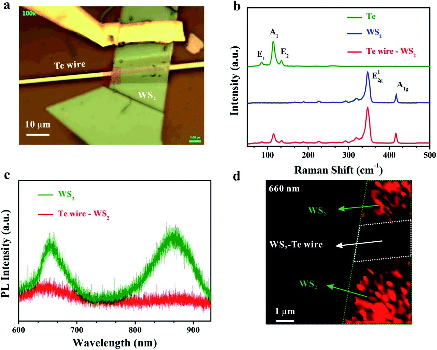 | ||
| Fig. 1 Raman and PL properties of the heterostructure. (a) Optical image of the mixed-dimensional device. (b) Raman spectrum of the Te microwire, WS2 and Te microwire–WS2. (c) PL spectrum of WS2 and Te microwire–WS2 under 532 nm laser excitation. (d) PL mapping of the WS2 nanosheet on the Te microwire located from the red rectangular region in (a). | ||
Raman scattering measurement was used to characterize the phonon vibrations and interlayer coupling of the Te microwire–WS2 mixed-dimensional heterostructure. Fig. 1b shows the Raman spectrum of the pristine Te microwire, WS2 and the heterostructure. The Te microwire shows three vibration peaks located at 85.6 cm−1, 115.2 cm−1 and 134.3 cm−1, which correspond to the in-plane E1, E2 and A1 (out-of-plane) vibrations, respectively.13 The in-plane E12g and out-of-plane A1g modes of the multilayered WS2 nanosheet are observed at 348.1 cm−1 and 418.7 cm−1, respectively.39 The Raman spectrum of the Te–WS2 vdW heterostructure exhibits the combination of phonon modes of both Te wire and WS2. Noticeably, the vibration modes of the overlapped Te are weakened. Interestingly, both vibration modes of WS2 are enhanced compared to those in the single part, which may be attributed to the strain effect.40Fig. 1c shows the PL of the WS2 and WS2–Te heterostructure with 532 nm laser excitation. In general, the exfoliated multilayered WS2 nanosheet shows two clear PL peaks at 660 nm and 861 nm, corresponding to a red-shifted direct optical band gap of 1.88 eV and an indirect band gap of ∼1.44 eV.39 A PL quenching effect is observed in the overlapped region for both PL peaks, which is ascribed to a strong interlayer coupling effect between Te and WS2. The PL quenching effect indicates that the photo-generated carrier separation process can be significantly accelerated under the designed type-II band alignment. Intuitively, Fig. 1d also displays the corresponding PL mapping image of the WS2 on the Te microwire from the rectangular area in Fig. 1a at 660 nm light excitation. The PL intensity of the WS2 nanosheet on top of the Te microwire (in the white area) becomes much weaker than that of WS2 without Te underneath (in green regions). A similar PL quenching effect is also observed from the PL mapping image under 860 nm light excitation shown in Fig. S3.†
The AFM image of the heterostructure is shown in Fig. 2a. The thickness of the WS2 nanosheet is estimated to be 50 nm shown in Fig. 2b. A Kelvin Probe Force Microscope (KPFM) was used to measure the built-in contact potential difference at the interface between the Te microwire and WS2. The surface potential distribution (SPD) along the area of the Te microwire, WS2 and the AFM tip can be expressed as the following equations:41
| eSPDWS2 = Wtip − WWS2 | (1) |
| eSPDTe = Wtip − WTe | (2) |
| ΔEf = WTe − WWS2 = eSPDWS2 − eSPDTe | (3) |
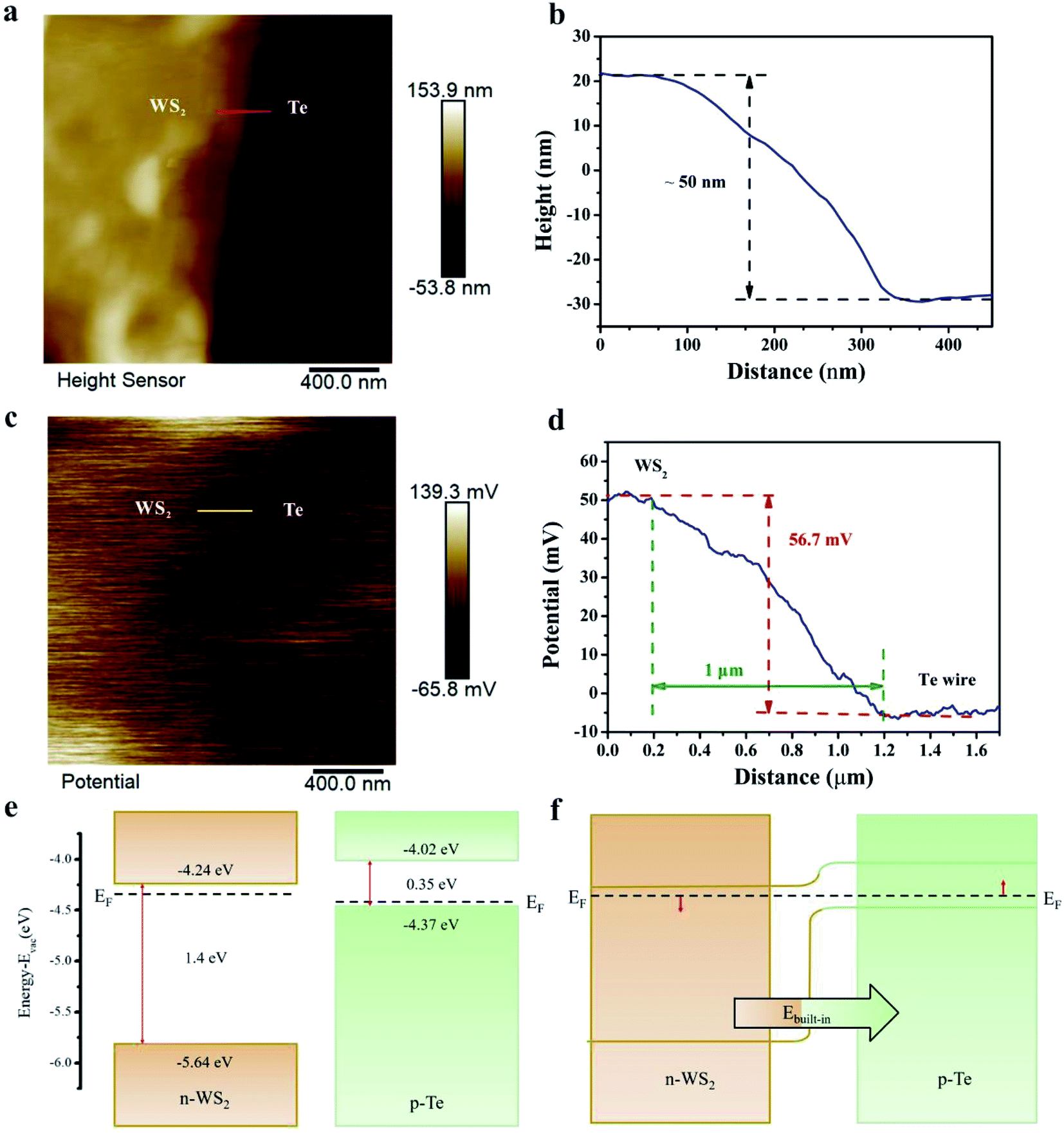 | ||
| Fig. 2 Characterization and band alignment analysis of the mixed-dimensional heterostructure. (a) AFM image of the WS2 nanosheet on the Te microwire. (b) The height data of the WS2 nanosheet along the scale length of the red line in (a). (c) Spatial potential distribution at the heterostructure interface. (d) The SPD along the yellow line in (c). (e) The energy band diagram of the Te microwire and WS2 heterostructure before contact and (f) after contact. | ||
Fig. 2c shows the topological image of the SPD of the heterostructure interface. The ΔEf and the depletion width along the yellow line are about 56.7 meV and 1 μm from Fig. 2d, which unveils a strong built-in electric field across the WS2–Te microwire interface.42–44 Moreover, the energy band alignments of the Te microwire and WS2 before and after contact are shown in Fig. 2e and f. In general, the indirect bandgaps of multilayered WS2 and Te are 1.4 eV and 0.35 eV, respectively. Before contact, the conduction band minima (CBMs) of the WS2 and Te microwire are approximately −4.24 eV and −4.02 eV, respectively, and the corresponding valence band maxima (VBMs) of the WS2 and Te microwire are approximately −5.64 eV and −4.37 eV, respectively.39,45 ΔEf is 56.7 meV from the KPFM measurement. Thus, the fabricated Te–WS2 heterostructure theoretically has a type-II (staggered gap) band arrangement attributing to the PL quenching effect, which can facilitate the photo-generated carrier generation and separation at the heterointerface.46 After contact, the band alignment becomes bent and the electrons and holes can transfer within interlayers via a built-in electric field pointing from n-WS2 to the p-Te microwire.47
The 3D diagram of the 635 nm laser-illuminated Te microwire–WS2 heterostructure is shown in Fig. 3a. In Fig. 3b, the mixed-dimensional heterostructure device exhibits n-type (electron dominated) transport behavior, demonstrating that the transport properties of the heterostructure mainly depend on the multilayered WS2 channel. Output characteristic curves of the device show that the drain current at a forward bias of 2 V monotonously increases as the Vg increases, which further confirms the n-type behavior and moderate gate modulation shown in Fig. 3c. The maximum rectification ratio of the device is ∼61 shown in Fig. S4c (ESI†). As a control, the transfer properties of the pristine Te microwire and multilayered WS2 nanosheet are shown in Fig. S4a and b (ESI†), where the Te microwire exhibits a strong p-type behavior with a current on/off ratio of ∼1.1 because of the ultra-narrow band gap of 0.35 eV, high conductivity in bulk and strong capacitance screening effect. Meanwhile, the multilayered WS2 nanosheet demonstrates a typical moderate n-type behavior with current on/off ratio of ∼103. Fig. 3d demonstrates the I–V curves of the mixed-dimensional heterostructure device in the range of −2 V to 0.3 V under dark conditions and 635 nm light illumination with various light power intensities. The significantly enhanced current under reverse bias compared to that under forward bias (majority carriers) is shown under light illumination because of the obviously increased minority carriers in the P–N junction. Under higher light power intensity, more photogenerated electron–hole pairs are separated by a built-in electric field and driven by the external reverse bias voltage resulting in the increment of photocurrent. The photovoltaic effect can be seen in Fig. 3d with obvious Voc and Isc, which indicates a well built-in electric field at the interface and will be discussed later.
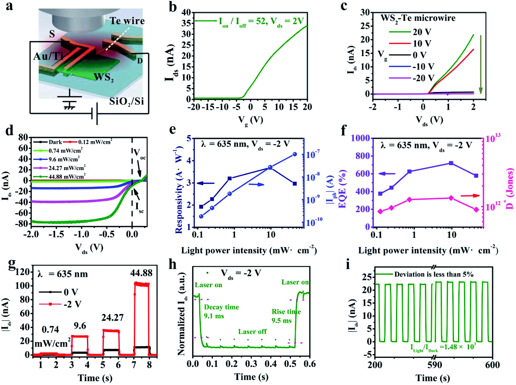 | ||
| Fig. 3 Electronic and optoelectronic properties of the heterostructure based device. (a) The 3D schematic diagram of the mixed-dimensional heterostructure photodetector under 635 nm light illumination. (b) The transfer curve of the device correlated with Vg. (c) Output characteristic curves of the device under Vg from 20 to −20 V. (d) I–V curves of the heterostructure device under dark conditions and 635 nm light illumination with various intensities. (e) Photoresponsivity and net photocurrent as a function of light power intensity. (f) EQE and D* dependence on incident light power intensity. (g) Time-dependent photocurrent of the device under different light power intensities at 0 and −2 V bias voltages, respectively. (h) Time-resolved photoresponse measurements. (i) On–off photoresponse with 200 cycles of the heterostructure based photodetector. | ||
To further evaluate the photodetection ability of the heterostructure, we calculated the photoresponsivity (Rλ), external quantum efficiency (EQE), detectivity (D*), response time and Ilight/Idark ratio of the device. In general, Rλ is used to evaluate the sensitivity of a photodetector, which is defined by the formula48
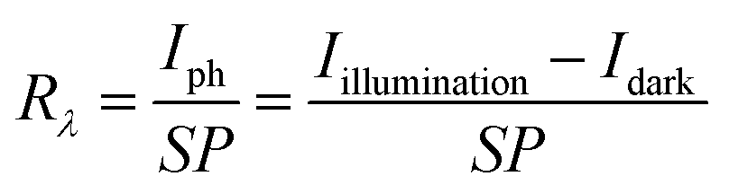 | (4) |
EQE is the ratio of the number of effective photogenerated carriers to the number of incident photons, which can be expressed as48
 | (5) |
Specific detectivity (D*) is an important figure of merit of a photodetector, which shows the ability of a photodetector to detect a weak light signal, as calculated by the following equation:41
 | (6) |
Fig. 3e displays the photoresponsivity and net photocurrent as a function of light power density. The photocurrent increases with increased light power intensity. From the fitting curve which follows a power law of photocurrent and light power intensity (Iph ∼ Pα), the exponent (α) value of 1.07 is obtained shown in Fig. S5 (ESI†). The super-linear behavior may be ascribed to the decrement of Auger recombination sites leading to more photocurrent being transmitted through the pn junction without the trapping effect.49 Furthermore, due to the limited trap states, the captured carriers are saturated or reduced under high light power intensity resulting in a significant decrease of the photoresponsivity and increased Auger recombination process.26 The maximum value of photoresponsivity reaches 3.6 A W−1 at a reverse bias of −2 V shown in Fig. 3e. Fig. 3f demonstrates the dependence of EQE and D* of the mixed-dimensional photodetector on the incident light power intensity. The maximum EQE and D* are 720% and 1.34 × 10¹² Jones, respectively. Fig. 3g illustrates the time-resolved response behaviors of the mixed-dimensional heterostructure with varying light power intensities at biases of 0 V (in black) and −2 V (in red). With higher light power intensity, more photogenerated electron–hole pairs can contribute to the photocurrent. Under a Vds of −2 V, the width of the depletion region is broadened and the corresponding built-in electric field of the heterostructure is enhanced.44 Therefore, the separation and collection of photogenerated electron–hole pairs are accelerated resulting in the increment of photocurrent and faster response time. Moreover, response time is one of the important parameters for the photodetector, which is defined as the time obtained from 10–90% (τrise is called rise time) to 90–10% (τdecay is called decay time) of the net photocurrent.48Fig. 3h illustrates the rise time of 9.5 ms and decay time of 9.1 ms at a bias of −2 V, which are comparable to or faster than that in previously reported 1D–2D mixed-dimensional heterostructures. The high electrical conductance of the Te microwire can contribute to the fast response speed and high responsivity as well in Fig. S4a (ESI†). As shown in Fig. 3i, the Ilight/Idark ratio of the device is as high as 103 at a bias of −2 V under light power intensity because of the low dark current in the PN junction. Furthermore, the deviation is less than 5% within 200 cycles for switching on–off behavior. In comparison, the Ilight/Idark ratio of pristine WS2 only reaches ∼20 due to a large dark current of around 10−9 A under −2 V bias. Meanwhile, the switching on–off curve of the WS2 nanosheet based photodetector exhibits poor stability shown in Fig. S4d (ESI†), which is mainly ascribed to the persistent photoconductive (PPC) effect in multilayered WS2.50 The photoresponse properties of the pristine WS2 nanosheet are shown in Fig. S6 and S7 (ESI†), which is worse than that in the heterostructure.
As we know, self-powered photodetectors are extensively desired in the field of wearable electronics and Internet of Things featuring lower power consumption or a self-sustaining wireless sensing network.51 Here, the self-powered photo-response properties of the mixed-dimensional heterostructure photodetector are intensively investigated to highlight the contact quality of the PN junction. The open-circuit voltage (Voc) of the device is induced by the built-in electric field because of the photogenerated holes accumulating at the n-WS2 side and electrons accumulating at the p-Te microwire side. Fig. 4a displays the Voc and Isc as a function of incident light power intensity. With higher light power intensity, the built-in electric field is strengthened leading to the nonlinear increase of Voc and the linear enhancement of Isc for the device. Fig. 4b shows the dependence of photocurrent and photoresponsivity on incident light power density. The maximum photoresponsivity of the self-powered heterostructure is as high as 471 mA W−1 under 0.74 mW cm−2. The exponent (α) values of 1.62 (under weak light) and 0.76 (under strong light) are obtained by fitting the measured data because of the complex transfer and recombination process of photo-carriers. Fig. 4c shows the incident light power intensity related EQE and D* of the device; the maximum EQE (91%) and D* (1.24 × 10¹² Jones) are obtained under 0.74 mW cm−2, respectively.
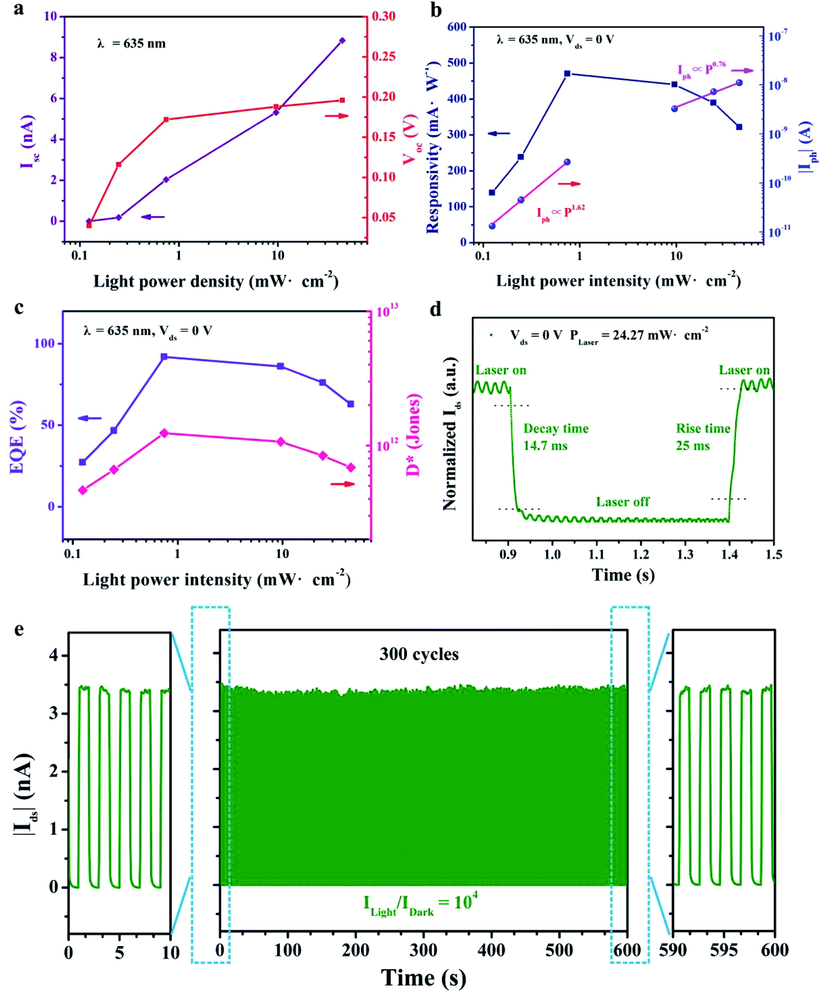 | ||
| Fig. 4 Self-powered photo-response characteristics of the heterostructure device under 635 nm illumination. (a) The Voc and Isc of the device versus illumination power intensity. (b) Photocurrent and Rλ varying with incident intensities under 0 V bias. (c) EQE and D* as a function of the light power intensity. (d) Rise and decay time of the device under 24.27 mW cm−2. (e) Photo-response of the photodetector with 300 cycles. | ||
The self-driven heterostructure device also exhibits a fast photoresponse time with a rise time of 25 ms and a decay time of 14.7 ms shown in Fig. 4d. Due to the faster speed of recombination of carriers than the generation and transport processes, the decay time is shorter than the rise time.52 As shown in Fig. 4e, the Ilight/Idark ratio is up to 104 at the dark current level of 3.1 × 10⁻¹³ A. Last but not least, the switching performance of the as-fabricated self-powered photodetector also shows negligible degradation after 300 cycles without obvious deviation. The photodetection parameters of the 1D Te–2D WS2 device compared with the previously reported 1D–2D mixed-dimensional heterostructure are shown in Table 1.
| Sample | Wavelength [nm] | V ds/Vg [V] | I light/Idark | Rise/decay time [ms] | R λ [mA W−1] | EQE [%] | D* [Jones] | Ref. |
|---|---|---|---|---|---|---|---|---|
| ZnO–WSe2 | 520 | −5/— | — | 50 | 670 | 160 | — | 25 |
| CuO–MoS2 | 570 | −2/0 | 103 | 34.6/51.9 | 157.6 | 157.6 × 10³ | — | 26 and 27 |
| Se–InSe | 460 | 0/0 | 103 | 30/37 | 110 | 51 | — | 29 |
| Te–MoS2 | 1550 | 2/80 | 103 | 15/32 | 106 | — | 1012 | 30 |
| ZnO–MoS2 | 532 | 5/0 | — | 140/8320 | 350 | 80.9 | — | 28 |
| Te–WS2 | 635 | −2/0 | 1480 | 9.5/9.1 | 3690 | 720 | 1.34 × 10¹² | This work |
| Te–WS2 | 635 | 0/0 | 104 | 25/14.7 | 471 | 91 | 1.24 × 10¹² | This work |
In addition, the photoresponsivity spectra of the mixed-dimensional heterostructure device at biases of −2 V and 0 V were also recorded and are shown in Fig. 5a. Notably, the photodetector displays a broadband photo-response ranging from 400 nm to 750 nm wavelength. Obviously, the strongest responsivity peaks are located at an approximately sharp edge of 620 nm under both conditions. The corresponding light power–wavelength diagram is shown in Fig. S8 (ESI†). The broadband photoresponse of the heterostructure device can be attributed to the highly efficient broadband optical absorption spectrum of the WS2 nanosheet.39 The photodetection properties of the mixed-dimensional heterostructure under 532 nm laser illumination were also investigated shown in Fig. S9 (ESI†). The different photoresponsivity between 532 nm and 635 nm incident light is related to the wavelength-dependence of light absorption and semiconductor energy gap.48 The photo-generated carrier transport dynamics mechanism under light illumination is illustrated in Fig. 5b. Under illumination, the photogenerated electron–hole pairs are induced in the depletion between WS2 and Te microwire interface. Meanwhile, photocurrent is generated through the separation of photo-generated electron–hole pairs in opposite directions to the metal electrode driven by the built-in electric field with and without external reverse bias voltage.47 Meanwhile, the non-radiative recombination rate is reduced within the band structure of the Te microwire.
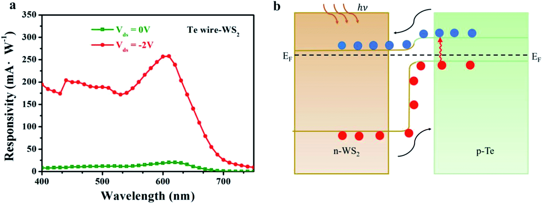 | ||
| Fig. 5 Wavelength-dependent photoresponse performance and the transport mechanism. (a) A broadband spectrum photoresponse behavior of the device. (b) Carrier transport dynamic mechanism of the mixed-dimensional photodetector under light illumination. | ||
Conclusions
In summary, a mixed-dimensional heterostructure based on the 1D Te microwire and 2D WS2 nanosheet has been fabricated for high performance photodetectors. Due to the built-in electric field and type-II band alignment, the heterostructure not only shows a fast photoresponse time (τrise = 25 ms, τdecay = 14.7 ms) but also an ultralow dark current level of 3.1 × 10⁻¹³ A compared with the pristine WS2 and Te microwire. The photodetection performances of the device under the biases of 0 V and −2 V are higher than or comparable to other reported 1D–2D mixed-dimensional heterostructure based photodetectors. The mixed-dimensional heterostructure can serve as a promising candidate for high performance self-powered photodetectors, promoting the development of 1D–2D hybrid systems for optoelectronic applications.Author contributions
W. Gao and J. B. Li designed the project and the experiments; L. X. Han performed the experiments and wrote the paper with help from W. Gao and N. J. Huo; the other authors discussed the results and helped to draw figures.Conflicts of interest
There are no conflicts to declare.Acknowledgements
This work was supported by the National Natural Science Foundation of China (No. 11904108 and No. 62004071), the China Postdoctoral Science Foundation (No. 2020M672680), and the “The Pearl River Talent Recruitment Program” (No. 2019ZT08X639).Notes and references
- K. S. Novoselov, A. K. Geim, S. V. Morozov, D. Jiang, Y. Zhang, S. V. Dubonos, I. V. Grigorieva and A. A. Firsov, Science, 2004, 306, 666 CrossRef CAS PubMed.
- K. S. Novoselov, A. K. Geim, S. V. Morozov, D. Jiang, Y. Zhang, S. V. Dubonos, I. V. Grigorieva and A. A. Firsov, Science, 2004, 306, 666 CrossRef CAS PubMed.
- K. S. Novoselov, D. Jiang, F. Schedin, T. J. Booth, V. V. Khotkevich, S. V. Morozov and A. K. Geim, Proc. Natl. Acad. Sci. U. S. A., 2005, 102, 10451 CrossRef CAS PubMed.
- A. K. Geim and K. S. Novoselov, Nat. Mater., 2007, 6, 183–191 CrossRef CAS PubMed.
- Q. H. Wang, K. Kalantar-Zadeh, A. Kis, J. N. Coleman and M. S. Strano, Nat. Nanotechnol., 2012, 7, 699–712 CrossRef CAS PubMed.
- S. Zhao, B. Dong, H. Wang, H. Wang, Y. Zhang, Z. V. Han and H. Zhang, Nanoscale Adv., 2020, 2, 109–139 RSC.
- H. Ying, X. Li, Y. Wu, Y. Yao, J. Xi, W. Su, C. Jin, M. Xu, Z. He and Q. Zhang, Nanoscale Adv., 2019, 1, 3973–3979 RSC.
- Y. Zhang, Q. You, W. Huang, L. Hu, J. Ju, Y. Ge and H. Zhang, Nanoscale Adv., 2020, 2, 1333–1339 RSC.
- M. Pumera and Z. Sofer, Adv. Mater., 2017, 29, 1605299 CrossRef PubMed.
- W. Tao, N. Kong, X. Ji, Y. Zhang, A. Sharma, J. Ouyang, B. Qi, J. Wang, N. Xie, C. Kang, H. Zhang, O. C. Farokhzad and J. S. Kim, Chem. Soc. Rev., 2019, 48, 2891–2912 RSC.
- T. Wang, H. Wang, Z. Kou, W. Liang, X. Luo, F. Verpoort, Y. J. Zeng and H. Zhang, Adv. Funct. Mater., 2020, 30 CAS.
- W. Gao, Z. Zheng, P. Wen, N. Huo and J. Li, Nanophotonics, 2020, 9, 2147–2168 CAS.
- E. J. Reed, nature, 2017, 552, 40–41 CrossRef CAS PubMed.
- Y. Wang, G. Qiu, R. Wang, S. Huang, Q. Wang, Y. Liu, Y. Du, W. A. Goddard, M. J. Kim, X. Xu, P. D. Ye and W. Wu, Nature Electronics, 2018, 1, 228–236 CrossRef.
- W. Wu, G. Qiu, Y. Wang, R. Wang and P. Ye, Chem. Soc. Rev., 2018, 47, 7203–7212 RSC.
- G. Qiu, Y. Wang, Y. Nie, Y. Zheng, K. Cho, W. Wu and P. D. Ye, Nano Lett., 2018, 18, 5760–5767 CrossRef CAS PubMed.
- X. Ren, Y. Wang, Z. Xie, F. Xue, C. Leighton and C. D. Frisbie, Nano Lett., 2019, 19, 4738–4744 CrossRef CAS PubMed.
- C. Shen, Y. Liu, J. Wu, C. Xu, D. Cui, Z. Li, Q. Liu, Y. Li, Y. Wang, X. Cao, H. Kumazoe, F. Shimojo, A. Krishnamoorthy, R. K. Kalia, A. Nakano, P. D. Vashishta, M. R. Amer, A. N. Abbas, H. Wang, W. Wu and C. Zhou, ACS Nano, 2020, 14, 303–310 CrossRef CAS PubMed.
- D. Jariwala, T. J. Marks and M. C. Hersam, Nat. Mater., 2017, 16, 170–181 CrossRef CAS PubMed.
- S. Mukherjee, S. Jana, T. K. Sinha, S. Das and S. K. Ray, Nanoscale Adv., 2019, 1, 3279–3287 RSC.
- P. Luo, F. Zhuge, F. Wang, L. Lian, K. Liu, J. Zhang and T. Zhai, ACS Nano, 2019, 13, 9028–9037 CrossRef CAS PubMed.
- J.-J. Tao, J. Jiang, S.-N. Zhao, Y. Zhang, X.-X. Li, X. Fang, P. Wang, W. Hu, Y. H. Lee, H.-L. Lu and D.-W. Zhang, ACS Nano, 2021, 15(2), 3241–3250 CrossRef CAS PubMed.
- Z. Q. Zheng, Y. Zhou, W. Gao, L. Zhang, M. Yang, J. Lu, Y. Zhao, J. Yao and J. Li, Nanoscale, 2021, 13, 5660–5669 RSC.
- D. Wang, X. Chen, X. Fang, J. Tang, F. Lin, X. Wang, G. Liu, L. Liao, J. C. Ho and Z. Wei, Nanoscale, 2021, 13, 1086–1092 RSC.
- Y. T. Lee, P. J. Jeon, J. H. Han, J. Ahn, H. S. Lee, J. Y. Lim, W. K. Choi, J. D. Song, M. C. Park, S. Im and D. K. Hwang, Adv. Funct. Mater., 2017, 27, 47 Search PubMed.
- P. Lin, L. Zhu, D. Li, L. Xu and Z. L. Wang, Nanoscale, 2018, 10, 14472–14479 RSC.
- D.-S. Um, Y. Lee, S. Lim, S. Park, H. Lee and H. Ko, ACS Appl. Mater. Interfaces, 2016, 8, 33955–33962 CrossRef CAS PubMed.
- J. Zhang, Y. Liu, X. Zhang, Z. Ma, J. Li, C. Zhang, A. Shaikenova, B. Renat and B. Liu, ChemistrySelect, 2020, 5, 3438–3444 CrossRef CAS.
- H. Shang, H. Chen, M. Dai, Y. Hu, F. Gao, H. Yang, B. Xu, S. Zhang, B. Tan, X. Zhang and P. Hu, Nanoscale Horiz., 2020, 5, 564–572 RSC.
- N. Li, Y. Wen, R. Cheng, L. Yin, F. Wang, J. Li, T. A. Shifa, L. Feng, Z. Wang and J. He, Appl. Phys. Lett., 2019, 114 Search PubMed.
- Y. Xiang, S. Gao, R.-G. Xu, W. Wu and Y. Leng, Nano Energy, 2019, 58, 202–210 CrossRef CAS.
- Y. Wang, S. Yao, P. Liao, S. Jin, Q. Wang, M. J. Kim, G. J. Cheng and W. Wu, Adv. Mater., 2020, 32, 29 Search PubMed.
- S. Gao, C. Sun and X. Zhang, Nanophotonics, 2019, 9, 1931–1940 CrossRef.
- S. Sharma, N. Singh and U. Schwingenschlögl, ACS Appl. Energy Mater., 2018, 1, 1950–1954 CrossRef CAS.
- G. Qiu, C. Niu, Y. Wang, M. Si, Z. Zhang, W. Wu and P. D. Ye, Nat. Nanotechnol., 2020, 15, 585–591 CrossRef CAS PubMed.
- S. Khatun, A. Banerjee and A. J. Pal, Nanoscale, 2019, 11, 3591–3598 RSC.
- A. Kramer, M. L. V. d. Put, C. L. Hinkle and W. G. Vandenberghe, npj 2D Mater. Appl., 2020, 4, 1–8 CrossRef.
- G. Zhou, R. Addou, Q. Wang, S. Honari, C. R. Cormier, L. Cheng, R. Yue, C. M. Smyth, A. Laturia, J. Kim, W. G. Vandenberghe, M. J. Kim, R. M. Wallace and C. L. Hinkle, Adv. Mater., 2018, 30(36), 1803109 CrossRef PubMed.
- R. Basnet, M. H. Doha, T. Hironaka, K. Pandey, S. Davari, K. M. Welch, H. O. H. Churchill and J. Hu, Crystals, 2019, 9, 486 CrossRef.
- C. Jia, X. Huang, D. Wu, Y. Tian, J. Guo, Z. Zhao, Z. Shi, Y. Tian, J. Jie and X. Li, Nanoscale, 2020, 12, 4435–4444 Search PubMed.
- A. Castellanos-Gomez, R. Roldán, E. Cappelluti, M. Buscema, F. Guinea, H. S. J. v. d. Zant and G. A. Steele, Nano Lett., 2013, 13, 5361–5366 CrossRef CAS PubMed.
- W. Gao, Z. Zheng, Y. Li, Y. Zhao, L. Xu, H. Deng and J. Li, Nanoscale, 2019, 11, 13309–13317 RSC.
- W. Gao, Z. Zheng, Y. Li, C. Xia, J. Du, Y. Zhao and J. Li, J. Mater. Chem. C, 2018, 6, 12509–12517 RSC.
- K. Chen, X. Wan, W. Xie, J. Wen, Z. Kang, X. Zeng, H. Chen and J. Xu, Adv. Mater., 2015, 27, 6431–6437 CrossRef CAS PubMed.
- M. Dai, H. Chen, F. Wang, M. Long, H. Shang, Y. Hu, W. Li, C. Ge, J. Zhang, T. Zhai, Y. Fu and P. Hu, ACS Nano, 2020, 14, 9098–9106 CrossRef CAS PubMed.
- F. Qin, F. Gao, M. Dai, Y. Hu, M. Yu, L. Wang, W. Feng, B. Li and P. Hu, ACS Appl. Mater. Interfaces, 2020, 12, 37313–37319 CrossRef CAS PubMed.
- Z. Zheng, X. Zu, Y. Zhang and W. Zhou, Materials Today Physics, 2020, 15(80), 100262 CrossRef.
- J. Lu, Z. Zheng, W. Gao, J. Yao, Y. Zhao, Y. Xiao, B. Wang and J. Li, J. Mater. Chem. C, 2019, 7, 12104–12113 RSC.
- M. Long, P. Wang, H. Fang and W. Hu, Adv. Funct. Mater., 2019, 29, 1803807 CrossRef.
- W. Gao, F. Zhang, Z. Zheng and J. Li, ACS Appl. Mater. Interfaces, 2019, 11, 19277–19285 CrossRef CAS.
- N. Huo, S. Yang, Z. Wei, S.-S. Li, J.-B. Xia and J. Li, Sci. Rep., 2015, 4, 5209 CrossRef PubMed.
- Q. Wang, C. Zhou and Y. Chai, Nanoscale, 2020, 12, 8109–8118 RSC.
Footnote |
| † Electronic supplementary information (ESI) available: A schematic diagram of the fabrication process of the mixed-dimensional heterostructure device; a SEM image of the device; a PL mapping image of the heterostructure; transfer properties and I–t characteristics; the photocurrent dependence on the light power intensity which follows a power law of the heterostructure; light power–wavelength diagram; photoresponse properties of the mixed-dimensional heterostructrue Te microwire and WS2 nanosheet based photodetector under an incident laser of 532 nm. See DOI: 10.1039/d1na00073j |
| This journal is © The Royal Society of Chemistry 2021 |