
 Open Access Article
 This Open Access Article is licensed under a Creative Commons Attribution-Non Commercial 3.0 Unported Licence
3D fluorescence confocal microscopy of InGaN/GaN multiple quantum well nanorods from a light absorption perspective†
Yan
Gu
ab,
Yu shen
Liu
 c,
Guofeng
Yang
*b,
Feng
Xie
d,
Chun
Zhu
b,
Yingzhou
Yu
b,
Xiumei
Zhang
b,
Naiyan
Lu
*b,
Yueke
Wang
b and
Guoqing
Chen
b
c,
Guofeng
Yang
*b,
Feng
Xie
d,
Chun
Zhu
b,
Yingzhou
Yu
b,
Xiumei
Zhang
b,
Naiyan
Lu
*b,
Yueke
Wang
b and
Guoqing
Chen
b
aSchool of Internet of Things, Jiangnan University, Wuxi 214122, China
bSchool of Science, Jiangsu Provincial Research Center of Light Industrial Optoelectronic Engineering and Technology, Jiangnan University, Wuxi 214122, China. E-mail: gfyang@jiangnan.edu.cn; lunaiyan@jiangnan.edu.ch
cSchool of Electronic and Information Engineering, Changshu Institute of Technology, Changshu 215556, China
dThe 38th Research Institute of China Electronics Technology Group Corporation, Hefei 230000, China
First published on 19th March 2021
Abstract
A nanostructure of In0.18Ga0.82N/GaN multiple quantum well (MQW) nanorods (NRs) was fabricated using top-down etching with self-organized nickel (Ni) nanoparticles as masks on the wafer. The optical properties of In0.18Ga0.82N/GaN MQW NRs were discussed by experiment and theory from a light absorption perspective. Three-dimensional (3D) optical images of NRs were successfully obtained by confocal laser scanning microscopy (CLSM) for physical observation of the optical phenomenon of InGaN/GaN MQW NRs. Moreover, optical simulations were performed by COMSOL Multiphysics via the three-dimensional finite-element method to explore the influences of NR geometrical parameters on optical absorption. The simulated results demonstrate that the absorption of NRs is higher than that of the film due to the waveguide properties of NRs resulting from their higher refractive index than embedding medium and higher aspect ratio than bulk. In addition, an increase in the diameter results in a red-shift of the absorption peak position of In0.18Ga0.82N/GaN MQW NRs. The smaller pitch enhances the near-field coupling of the nanorods and broadens the absorption peak. These results clearly illustrate the optical properties of In0.18Ga0.82N/GaN MQW NRs from the perspective of 3D confocal laser scanning microscopy. This work is promising for the applications of III–V optoelectronic devices.
Introduction
III–V semiconductor materials have excellent electrical and optical properties, such as direct band gap, high electron mobility and low effective mass.1–4 Therefore, in recent years, III–V nanostructures have attracted enormous interest due to their potentially significant applications in photovoltaics, photodetection, waveguide devices, and biosensing.5–10 In particular, the operating wavelengths of various devices constructed of III-nitride semiconductor materials cover the spectral range from near-infrared (NIR) to deep-ultraviolet (UV) spectrum because the bandgap can be adjusted in the range of 0.7–6.2 eV.4 InGaN/GaN multiple quantum wells (MQWs) have been viewed as the most promising active regions for the applications of light-emitting optical devices in the UV-NIR spectrum.11–13 Besides, InGaN/GaN MQW nanorods (NRs) can overcome the negative impacts of dislocations caused by large lattice mismatch.14–16 Therefore, high crystalline quality with nanostructured InGaN/GaN MQWs can be acquired to improve the light extraction efficiency and achieve efficient light absorption. Considering the controllability of the size and density of nickel (Ni) nanoparticles, self-organized Ni nanoparticles can be used as etching masks by rapid thermal annealing (RTA). As a result, the nanorods fabricated by the top-down etching method provide a feasible choice for the synthesis of nanorods.17–19 Furthermore, the special properties of nanostructures that carriers and photons are confined in the transverse directions and propagate freely in longitudinal direction20,21 can produce special optical phenomena. In addition, some reports22,23 on 3D PL imaging of the In0.18Ga0.82N/GaN MQW NRs are helpful for understanding the optical properties. In order to study the optical phenomena of nanorods, confocal laser scanning microscopy (CLSM) can be used to perform 3D scanning to understand the interaction between light and nanostructures. 3D imaging of nanostructures in a microscopic environment using confocal scanning microscopes24 has been extensively reported.The optical properties of nanostructured devices are not only affected by the complex refractive index of the material, but also by the geometry and size of the nanostructure.25–27 Previously, many theoretical reports have studied the light absorption and waveguide properties of nanostructured arrays.20,28–33 Other reported experiments20,21,31,33,34 also reveal that the absorption of nanostructure arrays is strongly influenced by geometrical parameters, which agrees well with the simulation results. These results28,29,32,35 illustrated that the absorptance of nanostructures is larger than that of thin-film materials. However, how light interacts with InGaN/GaN MQW NRs still needs to be explored, which will play an important role in future optoelectronic devices like nanorod solar cells and photodetectors. Particularly, InGaN/GaN MQW NRs can offer useful spectral regions for UV-NIR photodetectors in light detection and ranging systems due to the large band gap tunability from 0.7 to 3.4 eV. Apart from that, it can achieve broadband absorption of III–V semiconductor NR arrays for photovoltaic applications.
In this work, the optical properties of InGaN/GaN MQW NRs on a sapphire substrate are investigated by combining experimental and theoretical approaches. The InGaN/GaN MQW NRs were fabricated by the top-down etching approach with self-organized Ni nano-island masks on the MQW wafer. The characterizations of the InGaN/GaN MQW NRs were carried out by atomic force microscopy (AFM) and field emission scanning electron microscopy (FE-SEM). Moreover, 3D fluorescence confocal laser scanning microscopy was performed to analyze the optical properties of InGaN/GaN MQW NRs. The result demonstrates that the nanorod geometry parameters have an influence on its optical properties. On the other hand, theoretically, numerical simulations were carried out by COMSOL Multiphysics via the three-dimensional finite-element method to explore the optical absorptance of electromagnetic waves and light–matter interactions in the InGaN/GaN MQW NR arrays systematically. The results indicate that the optical absorption characteristics of InGaN/GaN MQW NRs are significantly affected by the nanorod geometry including diameter, pitch (spacing between NRs), and filling ratio, which coincides with the experimental results from 3D CLSM.
Methods
The InGaN/GaN MQW NRs were fabricated by the top-down etching method on a planar InGaN/GaN MQW wafer, which was grown on a c-plane sapphire substrate by a metal–organic chemical vapor deposition (MOCVD) system. The group-III sources originated from trimethylgallium and trimethylindium, and the group-V source originated from NH3. The MOCVD-grown InGaN/GaN MQW structure was composed of a 20 nm-thick low temperature GaN buffer layer, a 2 μm-thick n-GaN epitaxial layer grown at 1050 °C, emitting layers with five pairs of 4/10 nm-thick InGaN (well layer)/GaN (barrier layer) MQWs, and a 200 nm-thick GaN cap layer. It was similar to our previous report17 that after the growth of planar InGaN/GaN MQW wafer, the InGaN/GaN MQW NRs were prepared by dry etching using Ni nanoparticles as a mask on the wafer. Firstly, a 5 nm Ni thin film was deposited on the surface of the planar MQW wafer by electron-beam (EB) evaporation. Then, in order to form self-organized Ni nanoparticles on the surface of the wafer sample, the Ni film was annealed at a temperature of 800 °C for 3 min by using the RTA process. InGaN/GaN MQW NRs can be fabricated by the dry etching method with the self-organized Ni nanoparticles used as an etching mask, which is attributed to the great selective etching rate of Ni for GaN-based materials.36 An inductively coupled plasma-reactive ion etching (ICP-RIE) system with Cl2 and BCl3 etchant gases was employed to perform InGaN/GaN MQW etching. Finally, residual Ni nano-masks were removed by immersing the sample into dilute hydrochloric acid (HCl) solution. The schematic diagrams of the detailed fabrication processes for the InGaN/GaN MQW NRs are illustrated in Fig. 1.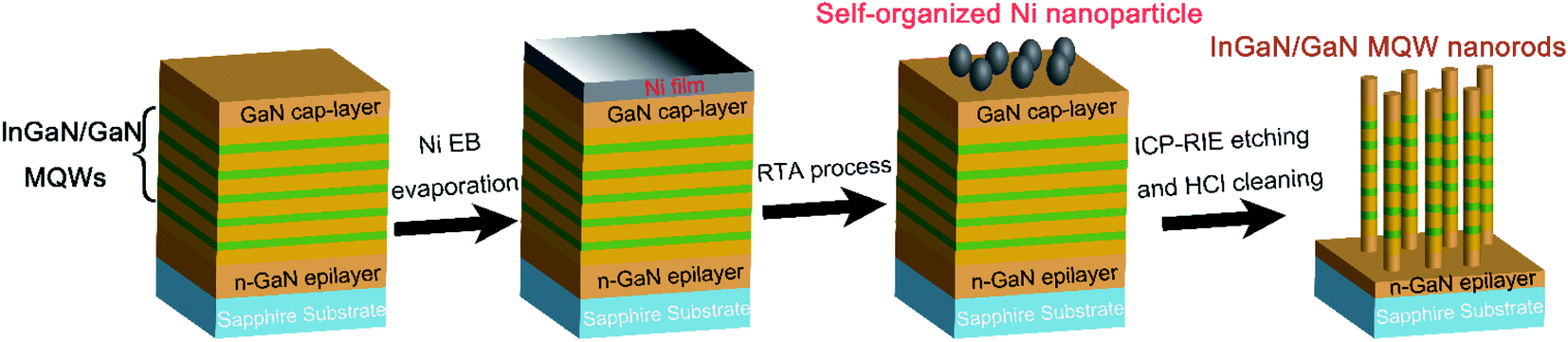 | ||
| Fig. 1 Schematic diagrams of the fabrication process for InGaN/GaN MQW nanorods. | ||
AFM and FE-SEM (ZEISS SIGMA 04-03) were used to characterize the self-assembled Ni nanoparticles and morphologies of fabricated InGaN/GaN MQW NRs. The photoluminescence (PL) property of the MQWs NRs at room temperature was measured by an Invia micro-Raman system (Renishaw LabRAM) with a 325 nm He–Cd excitation laser. A confocal laser scanning microscope (Zeiss CLSM 710) was used to obtain 2D images of nanorod arrays by scanning the laser beam (405 nm excitation) in the xy-plane, and obtain 3D images by acquiring z-stacks of xy-plane images with a vertical distance of 100 nm between each image. The nanorod images were obtained by using a 63× oil-immersion objective of numerical aperture of NA = 1.4 and image analysis was performed using ZEN 2008 software.
Theoretically, in order to explore the optical absorption properties of the InGaN/GaN MQW NR arrays, numerical simulations were performed by COMSOL Multiphysics with the finite-element method. In the finite element simulation, a plane wave of 405 nm corresponding to the wavelength of the laser applied for the confocal experiment was used as the incident light on the top of the NRs, which was parallel to the NR axis (z direction). The absorptance (A) of the nanorod can be obtained by solving the Helmholtz equations in three-dimensional optical simulation. Furthermore, the absorptance A(λ) is given by the equation:
| A(λ) = 1 − R(λ) − T(λ), | (1) |
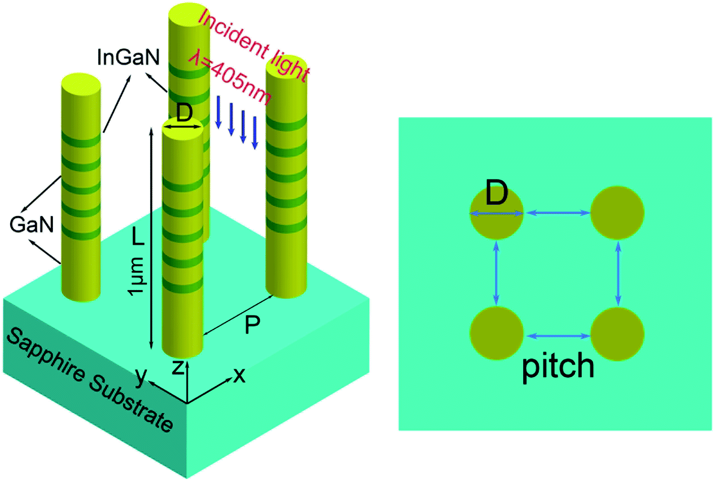 | ||
| Fig. 2 Schematic drawing of the periodic InGaN/GaN MQW NR array on a sapphire substrate. | ||
Results and discussion
Fig. 3(a) and (b) show the SEM images of fabricated In0.18Ga0.82N/GaN MQW NR arrays by ICP-RIE etching using self-organized Ni nano-island mask. It can be observed that the NRs reveal a vertical height of about 1.05 μm and a diameter width of 235 nm. In addition, several representative NRs have been chosen to study the variation of their width along the length of the NR and demonstrated that the size of these structures is below micrometers, which fit the “nano” criteria. Although the base is wider than the tip, the width is uniform at the distance is more than 400 nm from the top, so we approximate these structures as rods as a whole. Fig. 3(d) displays the normalized PL intensities of the InGaN/GaN MQW NRs at room temperature. The PL spectra exhibit an emission peak at about 449 nm (2.76 eV) with a full-width at half-maximum (FWHM) of about 141 meV. Since the fabricated nanorods are randomly distributed, the uniformity of the size of In0.18Ga0.82N/GaN MQW NRs and the effects on the optical properties for non-periodic NRs are discussed in Fig. S2 of ESI.† More details about the nanoscale self-assembly Ni islands by RTA at 800 °C for 3 min are shown in Fig. S3.†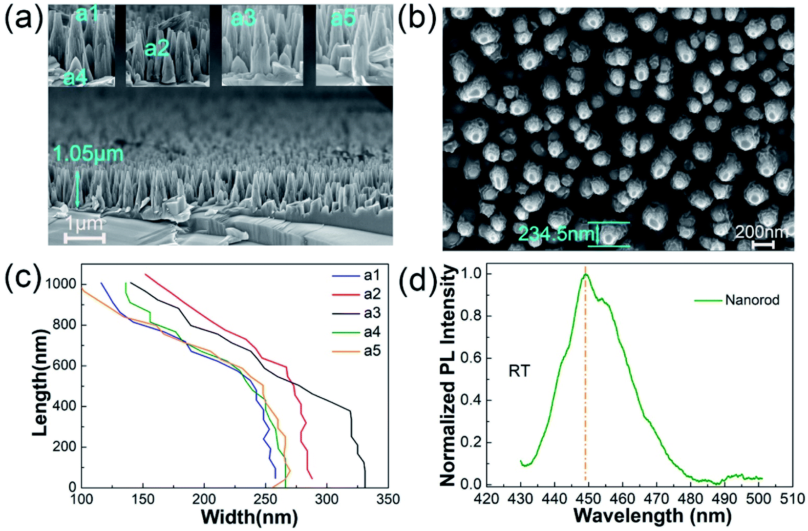 | ||
| Fig. 3 (a) Cross-sectional-view and (b) top-view SEM image of InGaN/GaN MQW NRs after ICP etching. (c) Width varies with length of the NRs. (d) PL spectra of the fabricated MQW NRs at room temperature. The insets in (a) show SEM images of several representative NRs. | ||
Fig. 4 displays the confocal pictures of NRs in XY, XZ and YZ planes at 8 bit resolution corresponding to the red lines on the XY image. It can be seen that the NRs can emit fluorescent light under the excitation of a 405 nm laser. The pinhole was set to one Airy unit, thus, the optical lateral resolution is Rxy = 176.5 nm and z-resolution is Rz = 289.3 nm. In addition, according to the confocal 3D image of the nanorod arrays, NRs with different pitches exhibit different optical phenomena that the luminous intensity around the NRs with a small pitch is stronger than that with a large pitch. Thus, we design different periodic array structures according to the various pitches of NRs shown in Fig. 4(a). Two different magnifications can be found in Fig. S3 of ESI.†
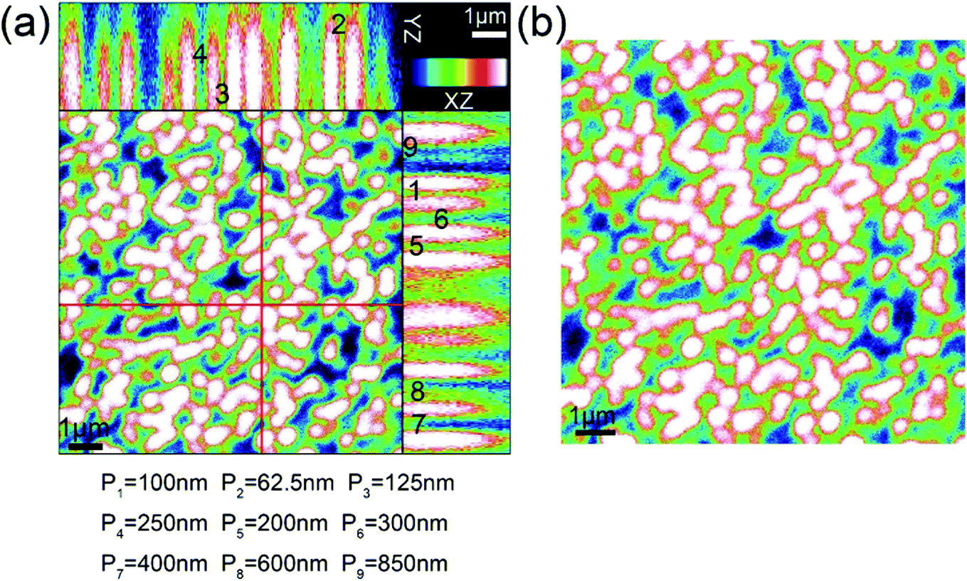 | ||
| Fig. 4 (a) Confocal XZ and YZ cross-sectional images of nanorod arrays with d = 235 nm and L = 1 μm derived by 100 nm z-stack in xy-plane. (b) Confocal xy slice of nanorods with different pitches excited by 405 nm laser. | ||
Fig. 5(a) shows the calculated total absorption spectra A(λ) of the InGaN/GaN MQW NR arrays with L = 1 μm, D = 235 nm and P = 100 nm using a plane wave with a wavelength ranging from 200 nm to 1000 nm. The simulated result indicates that a broad absorption peak appears in the InGaN/GaN MQW NRs due to effective couple of the incident light into HE11 and HE12 optical resonance modes for a large diameter of 235 nm. Besides, when the wavelength is larger than 440 nm, the absorption begins to decrease owing to transmission and reflection losses. The electric field distribution diagrams at the resonant wavelengths (λ = 315 and 440 nm) and non-resonant wavelengths (λ = 550 and 700 nm) are plotted in Fig. 5(b)–(f). The electric field intensity at the resonance mode has a significant maximum along the length of the nanorod. In addition, a part of the electric field exists around the nanorod. Therefore, light can be absorbed in the NRs. The electric field for λ = 315 nm shown in Fig. 5(b) is mainly localized on the top of the NRs and then decays rapidly, so that it cannot reach the bottom. On the other hand, the electric field for λ = 700 nm shown in Fig. 5(f) is mainly in air and hardly localized inside the nanorod, resulting in extremely low absorption. It can also be seen from the modal electric field diagrams shown in the insets that the mode at resonance (λ = 315 nm) is confined to the nanorod, while the mode at non-resonance (λ = 700 nm) is mostly in air, indicating a better confinement at resonance. The top-view electric field profiles at z = 120 nm are depicted in Fig. S4 (see ESI†).
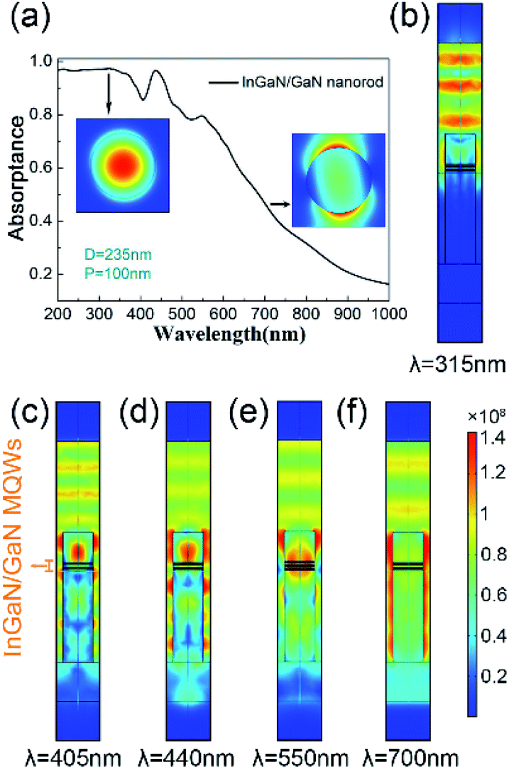 | ||
| Fig. 5 (a) Simulated total absorption spectra A(λ) of the vertical InGaN/GaN MQW NR arrays with L = 1 μm, D = 235 nm, and P = 100 nm. (b)–(f) xz-Plane electric field intensity distributions within nanorods at the resonant wavelengths and non-resonant wavelengths. The inset shows the electric field distributions of the fundamental mode at two representative wavelengths. | ||
The dependence of the InGaN/GaN MQW NR absorption on the NR pitch is displayed in Fig. 6(a). It is found that the absorptance (λ = 405 nm) reaches a maximum value of 92.1% for the nanorod array with a pitch of 50 nm. Furthermore, the absorption declines as the pitch increases, which would be attributed to the reason that as the pitch increases, the fill factors decrease and the near-field coupling becomes weaker. The electric field distributions of the xz-plane are plotted in Fig. 6(b)–(h), in order to analyse the reason for the decrease in absorption values. It is evident that the electric field within the NRs is weakened as the pitch increases. Therefore, the weak coupling of the NRs to light originating from the weak confinement of the electric field within the nanorods results in the decrease of absorption. The simulated results indicate that as the distance increases, the electric field in air becomes weaker, which agrees well with the experimental results with respect to the confocal observation that the light field intensity around the nanorod changes with the distance of neighbouring nanorods. The top view electric field distributions at z = 120 nm are depicted in Fig. S5.†
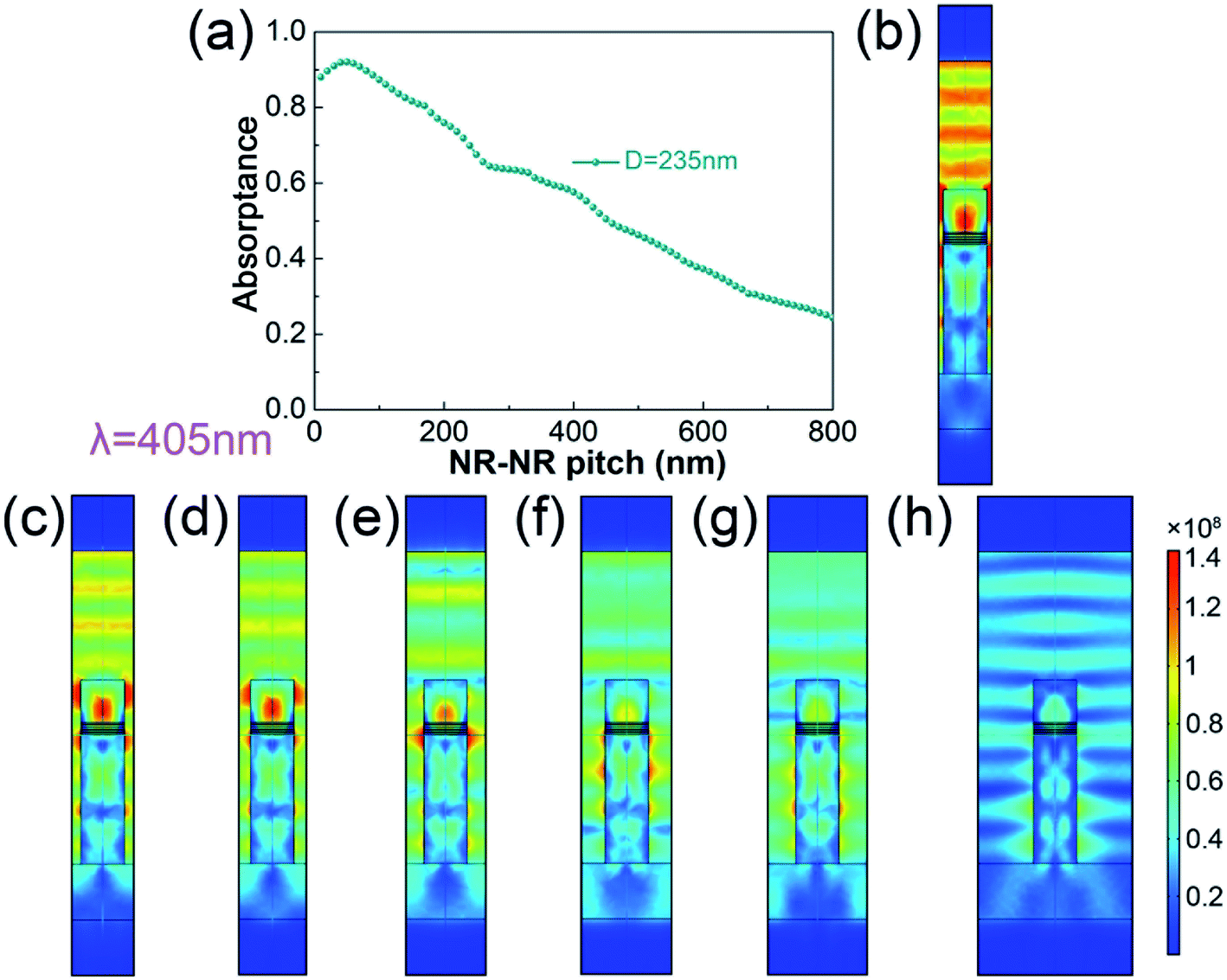 | ||
| Fig. 6 (a) The absorption of InGaN/GaN MQW NRs at λ = 405 nm with various pitches. (b)–(h) Electric field distributions of the nanorod arrays with different pitches. | ||
Since the internal resonance of the cylindrical nanostructures is mainly determined by diameters,20,29 it is necessary to study the influences of diameters on the optical properties of the InGaN/GaN MQW NRs. The variations in absorption with diameters for NRs are depicted in Fig. 7(a). It is found that the absorption of NRs is almost 0 at the diameter of 50 nm. With the increase in the diameter, the absorption begins to rise sharply around D = 75 nm, and a maximum value of 97.8% can be obtained at the diameter of 120 nm. However, the absorption decreases slightly as the diameter of the NRs continues to increase (>120 nm). The optical phenomenon can be explained by mode analysis and electric field distributions shown in Fig. 7(b)–(g). NRs with diameter that is much smaller than the ratio of the incident wavelength to the refractive index25 hardly support any mode due to the effective refractive index close to 1. The modal electric fields shown in the inset indicate that NRs with D = 50 nm and an effective refractive index of 1.02 cannot support fundamental mode, but the modal electric field can be well localized in the NRs with D = 120 nm. Therefore, as shown in Fig. 7(b), the incident plane wave is guided outside the NRs and transmits almost without interference from the NRs, resulting in the light not being absorbed in the NRs. The value of the effective refractive index can be >1 when the diameter of the NRs becomes larger, so that higher-order modes can appear in the NRs. As shown in Fig. 7(c)–(e), a larger electric field is obtained inside the NRs that induce the increase of absorption. The top view electric fields at z = 120 nm are shown in Fig. S6.†
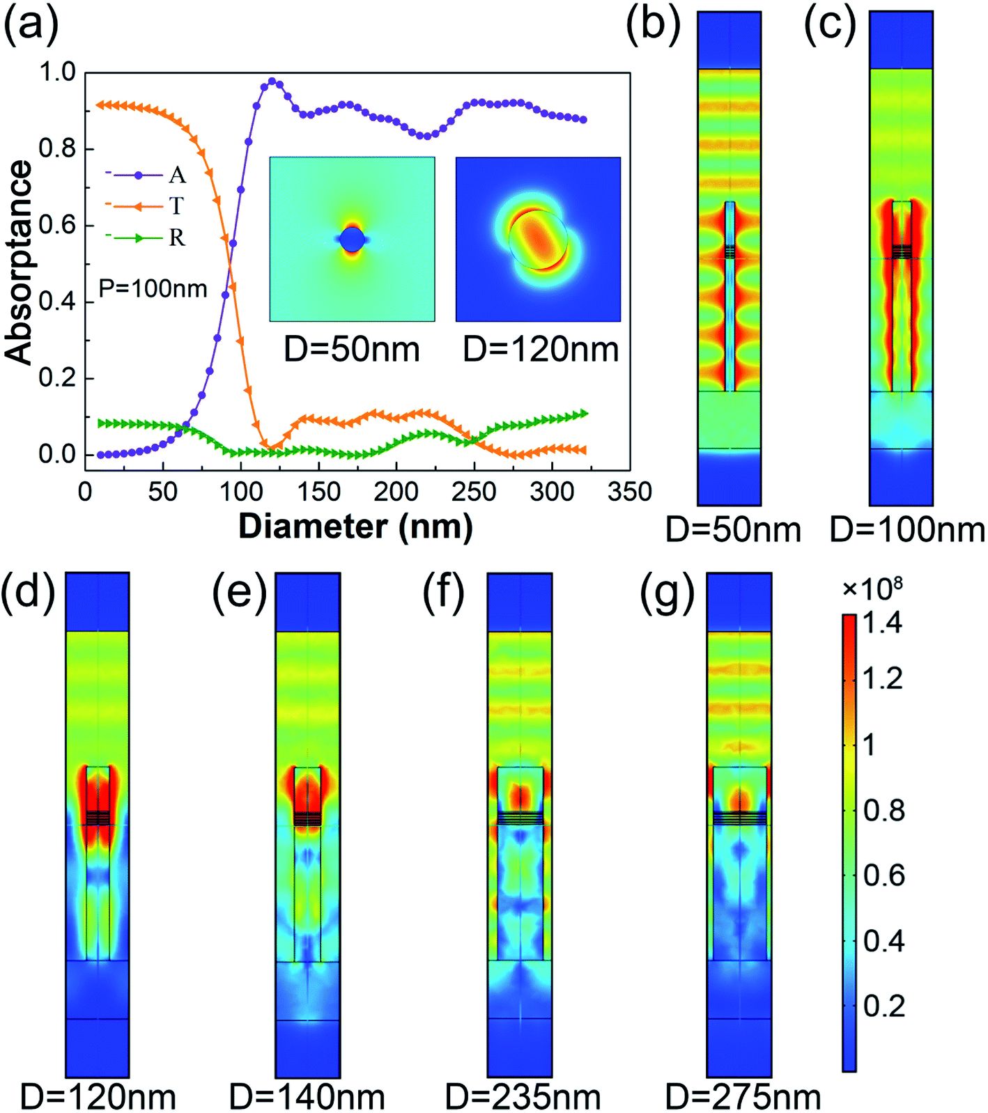 | ||
| Fig. 7 (a) A(λ), T(λ) and R(λ) of InGaN/GaN MQW NR arrays with L = 1 μm and P = 100 nm vary as a function of the NR diameter with incident plane wave of λ = 405 nm corresponding to the experimental excitation light. (b)–(g) Cross-sectional distribution diagrams of the NR electric field with different diameters. The inset shows the electric field distributions of fundamental mode at two D = 50 nm and 120 nm. | ||
Fig. 8(a) shows the relationship between the NR absorption and diameters at different NR pitches. The trend in the variation of absorption related to the change in the diameter is almost independent from the NR-to-NR pitch. Apart from that the absorption of InGaN/GaN MQW NR arrays with P = 50 nm and D = 125 nm to 250 nm is higher due to the large fill factor. The higher absorption can be obtained at D = 120 nm and P = 125 nm (200 nm). We also simulated the absorption spectrum of GaN nanorod array with D = 120 nm shown in Fig. 8(b). The results indicate that the wavelength at 355 nm contributes to the overall absorption of the GaN NRs because of good coupling of the incident light into the NRs. Fig. 8(b) illustrates the influences of NR diameter on the absorption spectrum. The results indicate that the absorption is the smallest for the diameter of 50 nm; nevertheless, the absorption of NR is higher than that of the plane MQW film due to enhanced light–matter interactions. It can be seen from the modal field in Fig. S7† that most light cannot be coupled into NRs with a small diameter, and more modes can be supported by increasing the diameter of NRs, so the absorption increases greatly. In addition, the high-absorption region shifts to longer wavelengths, and the absorption peak position is red-shifted with the increase of diameter. Moreover, the oscillation of the simulated absorption curve is attributed to the Fabry–Perot resonance. The diameter of 120 nm for NR was fixed to investigate the effect of spacing on the absorption spectrum according to the simulated results shown in Fig. 8(a) and (b). Fig. 8(c) presents the absorption spectra of nanorod arrays with different periods. The calculated results reveal that the absorption peaks begin to broaden as the NRs approach each other due to the mutual coupling of the resonance modes of the neighbouring NRs with close distance. Therefore, the near-field coupling of the NRs would induce the increase of absorption. Besides, the absorption peak position exhibits a slight red shift with the increased distance. It also can be found that when the pitch is more than 500 nm, the absorption peak position remains constant with decreased absorption due to the weak coupling and small filling factor.
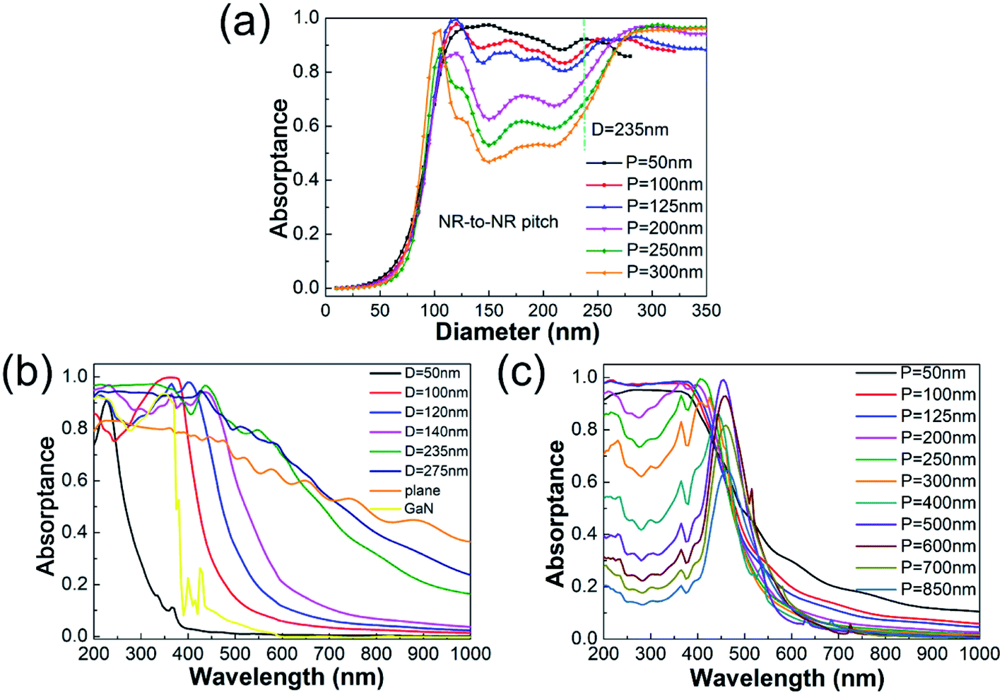 | ||
| Fig. 8 (a) The diameter-dependent absorption varies with NR spacing at λ = 405 nm. (b) The diameter-dependent absorption spectral curves of NR arrays with D ranging from 50 nm to 275 nm (P + D = 335 nm), and the referential absorption spectrum of the plane InGaN/GaN MQW film. (c) The pitch-dependent absorption spectrum of NR arrays with D = 120 nm. | ||
Conclusion
In summary, the optical properties of InGaN/GaN MQW NRs fabricated by top-down dry etching with Ni nano masks are discussed experimentally and theoretically from a CLSM perspective. The geometric parameters of InGaN/GaN MQW NRs including diameter of 235 nm and length of 1.05 μm are obtained. The In-content can be estimated to be 0.18 according to the peak position of the PL spectrum at room temperature. 3D images for understanding the interaction between light and nanostructures obtained by CLSM demonstrate that the NR geometry plays an important influence on its optical properties. Therefore, the effects of NR geometric parameters on light–matter interactions in the In0.18Ga0.82N/GaN MQW NR arrays are investigated systematically by optical simulations. The simulated results indicate that the absorption of the NR exceeds that of the referential plane MQW film with the same structure due to its optical waveguiding properties. In agreement with the result of CLSM experiment, since the pitch of neighbouring NRs affects the near-field coupling and fill factor, the electric field of the NRs becomes stronger and the absorption increases with the decrease in the distance of neighbouring NRs at an excitation of λ = 405 nm. It is also found that the absorption peak position shows a red-shift with the increase of NR diameter. Additionally, the pitch-dependent absorption spectra indicate that the absorption peak broadens owing to the enhanced near-field coupling of the neighbouring NRs. These results provide guiding suggestions for the design of InGaN/GaN MQW NR optoelectronic devices.Conflicts of interest
The authors declare no competing financial interest.Acknowledgements
This work was funded by the National Natural Science Foundation of China (Grant No. 61974056), Natural Science Foundation of Jiangsu Province (No. BK20190576), the Key Research and Development Program of Jiangsu Province (No. BE2020756), the National First-class Discipline Program of Food Science and Technology (Grant No. JUFSTR20180302), the Fundamental Research Funds for Central Universities (No. JUSRP22032), the Science and Technology Development Foundation of Wuxi (No. N20191002), the Postgraduate Research & Practice Innovation Program of Jiangsu Province (No. KYCY20_1769) and the Undergraduate Innovation and Entrepreneurship Training Program of Jiangsu Province (No. 202010295125Y).Notes and references
- D. H. Wang, C. Chen Huang, X. Liu, H. C. Zhang, H. B. Yu, S. Fang, B. S. Ooi, Z. Mi, J. H. He and H. D. Sun, Adv. Opt. Mater., 2020, 2000893 Search PubMed.
- H. M. Kim, D. S. Kim, D. Y. Kim, T. W. Kang, Y. H. Cho and K. S. Chung, Appl. Phys. Lett., 2002, 81, 2193–2195 CrossRef CAS.
- S. Nakamura, Science, 1998, 281, 956–961 CrossRef CAS PubMed.
- Y. R. Wu, C. H. Chiu, C. Y. Chang, P. C. Yu and H. C. Kuo, IEEE J. Sel. Top. Quantum Electron., 2009, 15, 1226–1233 CAS.
- S. L. Diedenhofen, O. T. A. Janssen, G. Grzela, E. Bakkers and J. G. Rivas, ACS Nano, 2011, 5, 2316–2323 CrossRef CAS PubMed.
- R. S. Frederiksen, E. Alarcon-Llado, P. Krogstrup, L. Bojarskaite, N. Buch-Manson, J. Bolinsson, J. Nygard, A. F. I. Morral and K. L. Martinez, ACS Photonics, 2016, 3, 1208–1216 CrossRef CAS.
- R. S. Frederiksen, E. Alarcon-Llado, M. H. Madsen, K. R. Rostgaard, P. Krogstrup, T. Vosch, J. Nygard, A. F. I. Morral and K. L. Martinez, Nano Lett., 2015, 15, 176–181 CrossRef CAS PubMed.
- D. Y. Guo, Q. X. Guo, Z. W. Chen, Z. P. Wu, P. G. Li and W. H. Tang, Mater. Today Phys., 2019, 11, 100157 CrossRef.
- D. Verardo, F. W. Lindberg, N. Anttu, C. S. Niman, M. Lard, A. P. Dabkowska, T. Nylander, A. Mansson, C. N. Prinz and H. Linke, Nano Lett., 2018, 18, 4796–4802 CrossRef CAS PubMed.
- J. Wallentin, N. Anttu, D. Asoli, M. Huffman, I. Aberg, M. H. Magnusson, G. Siefer, P. Fuss-Kailuweit, F. Dimroth, B. Witzigmann, H. Q. Xu, L. Samuelson, K. Deppert and M. T. Borgstrom, Science, 2013, 339, 1057–1060 CrossRef CAS PubMed.
- H. Sun, S. Mitra, R. C. Subedi, Y. Zhang, W. Guo, J. Ye, M. K. Shakfa, T. K. Ng, B. S. Ooi, I. S. Roqan, Z. Zhang, J. Dai, C. Chen and S. Long, Adv. Funct. Mater., 2019, 29, 1905445 CrossRef CAS.
- J. Piprek and Z. M. S. Li, Appl. Phys. Lett., 2013, 102, 023510 CrossRef.
- N. S. Yu, L. W. Guo, H. Chen, Z. G. Xing, J. Wang, X. L. Zhu, M. Z. Peng, J. F. Yan, H. Q. Jia and J. M. Zhou, Chin. Phys. Lett., 2006, 23, 2243–2246 CrossRef CAS.
- K. A. Dick, S. Kodambaka, M. C. Reuter, K. Deppert, L. Samuelson, W. Seifert, L. R. Wallenberg and F. M. Ross, Nano Lett., 2007, 7, 1817–1822 CrossRef CAS PubMed.
- T. Hino, S. Tomiya, T. Miyajima, K. Yanashima, S. Hashimoto and M. Ikeda, Appl. Phys. Lett., 2000, 76, 3421–3423 CrossRef CAS.
- K. L. Kavanagh, Semicond. Sci. Technol., 2010, 25, 024006 CrossRef.
- G. F. Yang, Y. Guo, H. X. Zhu, D. W. Yan, G. H. Li, S. M. Gao and K. X. Dong, Appl. Surf. Sci., 2013, 285, 772–777 CrossRef CAS.
- E. Barrigon, M. Heurlin, Z. X. Bi, B. Monemar and L. Samuelson, Chem. Rev., 2019, 119, 9170–9220 CrossRef CAS PubMed.
- C. H. Chiu, M. H. Lo, T. C. Lu, P. C. Yu, H. W. Huang, H. C. Kuo and S. C. Wang, J. Lightwave Technol., 2008, 26, 1445–1454 CAS.
- N. Dhindsa, A. Chia, J. Boulanger, I. Khodadad, R. LaPierre and S. S. Saini, Nanotechnology, 2014, 25, 305303 CrossRef PubMed.
- M. Khorasaninejad, S. Patchett, J. Sun, N. O and S. S. Saini, J. Appl. Phys., 2013, 114, 024304 CrossRef.
- W. Chen, X. Wen, M. Latzel, M. Heilmann, J. Yang, X. Dai, S. Huang, S. Shrestha, R. Patterson, S. Christiansen and G. Conibeert, ACS Appl. Mater. Interfaces, 2016, 8, 31887–31893 CrossRef CAS PubMed.
- W. J. Chen, X. M. Wen, J. F. Yang, M. Latzel, R. Patterson, S. J. Huang, S. Shrestha, B. H. Jia, D. J. Moss, S. Christiansen and G. Conibeer, Nanoscale, 2018, 10, 5358–5365 RSC.
- R. Frederiksen, G. Tutuncuoglu, F. Matteini, K. L. Martinez, A. F. I. Morral and E. Alarcon-Llado, ACS Photonics, 2017, 4, 2235–2241 CrossRef CAS PubMed.
- C. Hauswald, I. Giuntoni, T. Flissikowski, T. Gotschke, R. Calarco, H. T. Grahn, L. Geelhaar and O. Brandt, ACS Photonics, 2017, 4, 52–62 CrossRef CAS.
- B. E. A. Saleh and M. C. Teich, Fundamentals of Photonics, Wiley, 2007, vol. 45, p. 87 Search PubMed.
- R. Yan, D. Gargas and P. Yang, Nat. Photonics, 2009, 3, 569–576 CrossRef CAS.
- K. M. Azizur-Rahman and R. R. LaPierre, Nanotechnology, 2015, 26, 295202 CrossRef CAS PubMed.
- H. M. Guo, L. Wen, X. H. Li, Z. F. Zhao and Y. Q. Wang, Nanoscale Res. Lett., 2011, 6, 617 CrossRef PubMed.
- S. Mokkapati, D. Saxena, H. H. Tan and C. Jagadish, Sci. Rep., 2015, 5, 15339 CrossRef CAS PubMed.
- J. Treu, X. Xu, K. Ott, K. Sailer, G. Abstreiter, J. J. Finley and G. Koblmuller, Nanotechnology, 2019, 30, 495703 CrossRef CAS PubMed.
- L. Wen, Z. Zhao, X. Li, Y. Shen, H. Guo and Y. Wang, Appl. Phys. Lett., 2011, 99, 143116 CrossRef.
- P. M. Wu, N. Anttu, H. Q. Xu, L. Samuelson and M. E. Pistol, Nano Lett., 2012, 12, 1990–1995 CrossRef CAS PubMed.
- J. Zhang, N. Dhindsa, A. Chia, J. Boulanger and R. Lapierre, Appl. Phys. Lett., 2014, 105, 123113-1–123113-4 Search PubMed.
- J. Kupec, R. L. Stoop and B. Witzigmann, Opt. Express, 2010, 18, 27589–27605 CrossRef CAS PubMed.
- L. B. Chang, S. S. Liu and M. J. Jeng, Jpn. J. Appl. Phys., Part 1, 2001, 40, 1242–1243 CrossRef CAS.
- Y. Hu, R. R. LaPierre, M. Li, K. Chen and J. J. He, J. Appl. Phys., 2012, 112, 104311 CrossRef.
- S. Adachi, J. Appl. Phys., 1982, 53, 5863–5869 CrossRef CAS.
- J. Piprek, Semiconductor Optoelectronic Devices: Introduction to Physics and Simulation, UCSB: Academic., 2003, vol. 93 Search PubMed.
- G. F. Brown, J. W. Ager, W. Walukiewicz and J. Wu, Sol. Energy Mater. Sol. Cells, 2010, 94, 478–483 CrossRef CAS.
- T. Kawashima, H. Yoshikawa, S. Adachi, S. Fuke and K. Ohtsuka, J. Appl. Phys., 1997, 82, 3528–3535 CrossRef CAS.
- J. Wu, W. Walukiewicz, K. M. Yu, J. W. Ager, E. E. Haller, H. Lu, W. J. Schaff, Y. Saito and Y. Nanishi, Appl. Phys. Lett., 2002, 80, 3967–3969 CrossRef CAS.
Footnote |
| † Electronic supplementary information (ESI) available. See DOI: 10.1039/d1na00127b |
| This journal is © The Royal Society of Chemistry 2021 |