
 Open Access Article
 This Open Access Article is licensed under a Creative Commons Attribution-Non Commercial 3.0 Unported Licence
Detection of sub-atomic movement in nanostructures†
Tongjun
Liu
 a,
Jun-Yu
Ou
*a,
Kevin F.
MacDonald
*a and
Nikolay I.
Zheludev
ab
a,
Jun-Yu
Ou
*a,
Kevin F.
MacDonald
*a and
Nikolay I.
Zheludev
ab
aOptoelectronics Research Centre & Centre for Photonic Metamaterials, University of Southampton, SO17 1BJ, UK. E-mail: bruce.ou@soton.ac.uk; kfm@orc.soton.ac.uk
bCentre for Disruptive Photonic Technologies & the Photonics Institute, Nanyanag Technological University, 637371, Singapore
First published on 25th February 2021
Abstract
Nanoscale objects move fast and oscillate billions of times per second. Such movements occur naturally in the form of thermal (Brownian) motion while stimulated movements underpin the functionality of nano-mechanical sensors and active nano-(electro/opto) mechanical devices. Here we introduce a methodology for detecting such movements, based on the spectral analysis of secondary electron emission from moving nanostructures, that is sensitive to displacements of sub-atomic amplitude. We demonstrate the detection of nanowire Brownian oscillations of ∼10 pm amplitude and hyperspectral mapping of stimulated oscillations of setae on the body of a common flea. The technique opens a range of opportunities for the study of dynamic processes in materials science, nanotechnology and biology.
Introduction
Electromagnetic and quantum forces become stronger as the physical dimensions of objects decrease (e.g., the Coulomb force vs. separation between two electrons) and at sub-micron scales they begin to compete with weakening forces of elasticity. Movements also become faster as mass decreases with size, reaching Gigahertz frequencies at the nanoscale.1,2 These considerations present substantial technological opportunity and explain the growing interest in the fundamentals of nano-to atomic-scale dynamics3,4 and applications of nanomechanics to electronics and photonics.5,6 Exciting new functionalities emerge through the exploitation of nanomechanical movements in photonic metamaterials with variable optical properties achieved by nanoscale movements of artificial “meta molecules”.1,7–9 Entropic forces, Brownian motion, cooperative dynamics,10 quantum effects, and Casimir and Van der Waals interactions play important roles in nano- to atomic-scale dynamics.11 Over the last decade, protein (molecular) nanomechanics has seen tremendous progress, evolving into a burgeoning field of biochemical research, while there is considerable interest in adopting bio-inspired solutions in advanced materials, nanostructures and bionics.12,13 However, there are no routinely available imaging technologies that can quantitatively detect and spatially map fast, complex movements with sub-atomic amplitudes in nano-objects.14 Conventional electron and scanning probe microscopies, for example, routinely provide nano-to sub-nanometre spatial (imaging) resolution but can operate only at low frame rates, typically of not more than a few tens per second.15 Here we report on a technique that allows detection of movements of sub-atomic amplitude, and for spatial mapping of such movements with the nanometric image-plane resolution of a scanning electron microscope.Results and discussion
In scanning electron microscopy, a static image of an object is typically created by raster scanning a focused beam of free electrons over the object and detecting the secondary electron emission current I(r), where r is positional coordinate, integrated over a certain time interval at each pixel. This routinely delivers an image with nanoscale resolution, predominantly dependent on the focal spot size of the incident electron beam. However, at every point in the image plane and at time scales shorter than the per-pixel integration interval, the secondary electron current is sensitive to small (e.g., Brownian) movements δr(t) of the object (Fig. 1), giving rise to changes in current proportional to its gradient in the displacement direction: δI(r,t) ∼ (∇I(r) × δr(t)). Since I(r) is measured in the conventional mode of secondary electron imaging, ∇I(r) can readily be evaluated, and then from measurements of δI(r,t) at any/every point, movements δr(t) of the object can be detected and quantified. Displacements of picometric amplitude – smaller by orders of magnitude than the electron beam spot size – can be resolved in this way, as will be shown below.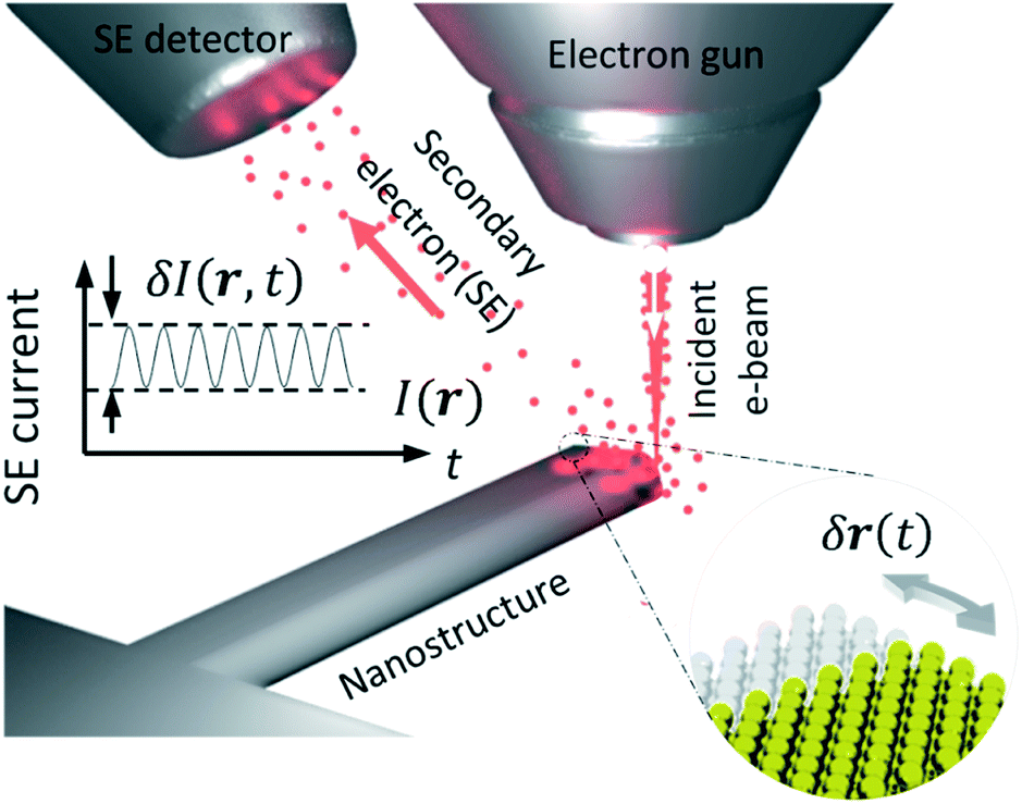 | ||
| Fig. 1 Detecting movement in nanostructures. When a beam of free electrons is focused at the edge of an oscillating nanostructure, the secondary electron current I(r,t) is modulated proportionally to the amplitude of movement δr(t) and the gradient of its secondary electron emission profile at the incident electron injection point. Spectral analysis of the current as a function of spatial coordinate r over the object provides for mapping the oscillatory modes of the nanostructure. | ||
To estimate the resolution of the technique, we assume that noise in the secondary electron current originates from the Poisson statistics of electrons incident on the detector. The signal-to-noise ratio (SNR) is then  where N is the number of detected electrons, e is electronic charge and τ is integration time. The secondary electron current gradient will be at a maximum at the sharp edges of a structure and limited by the spot size ρ of the incident electron beam. It can therefore be estimated as ∇I(r) ∼ I/ρ. When measuring the amplitude of displacement a ∼ |δr(t)| by detecting secondary electron current variation, unitary SNR will be achieved when
 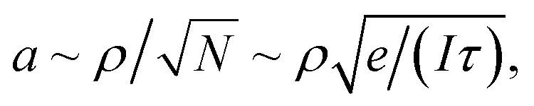 giving an estimate of the resolution of the technique. For the typical values in a scanning electron microscope: I ∼ 1 pA and ρ ∼ 1 nm, a displacement of a ∼0.4 pm could be measured with a one second integration time. By comparison, the lattice constants of solids are typically in the range from 300 to 700 pm and, by most definitions, the radii of isolated neutral atoms lie in the range between 30 and 300 pm.16
A point-by-point Fourier analysis of the secondary electron current provides for spatial mapping of the oscillatory modes of an object with nanoscale resolution determined by the focal spot size of the incident electron beam. This hyperspectral mode mapping can be performed within the bandwidth of the secondary electron detector and can enable mapping of Brownian motion in nanostructures. From thermodynamic considerations (the equipartition theorem), the root mean square (RMS) amplitude of Brownian motion for an oscillator with natural frequency f and effective mass meff is given by 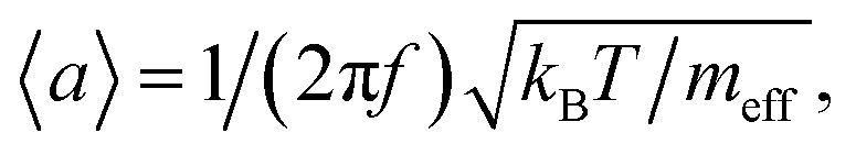 where kB is the Boltzmann constant and T is temperature. For example, a doubly clamped silicon nanowire 25 μm long and 200 nm × 200 nm in cross-section will have effective mass ∼9.28 × 10⁻¹⁶ kg (the ratio of its effective mass and its physical mass is 0.4 in its fundamental mode17) and will oscillate at fundamental frequency f ∼ 3 MHz. At room temperature (T ∼ 300 K) it will exhibit thermal oscillations of RMS amplitude 〈a〉 ∼100 pm.
Application of the motion detection technique to the study of Brownian motion in nanostructures is illustrated in Fig. 2. The test structure consists of an array of nanowire beams of different lengths cut from a 50 nm thick silicon nitride membrane coated in a further-structured 50 nm layer of gold (as archetypal elements of, for example, a nano-mechanical photonic metamaterial). The beams range in length from 20 to 30 μm in 2 μm steps and have fundamental in-plane oscillation frequencies of between 2.11 and 1.17 MHz. With the incident electron beam (acceleration voltage 5 kV, beam current 86 pA) focused to a point at the edge of the central section of a beam, and with knowledge of the secondary electron current gradient ∇I at that point from the static image (DC component of the SE signal) of the sample I(r), the frequency dispersion of calibrated in-plane Brownian displacement amplitude (Fig. 2b) can be derived from the measured frequency spectrum of secondary electron current δr(ω) ∼ δI(ω)/∇I. The optimum injection point for each nanowire is selected on the basis of SNR (over an 18 ms integration time) from a line scan of several points traversing the high secondary electron gradient edges.
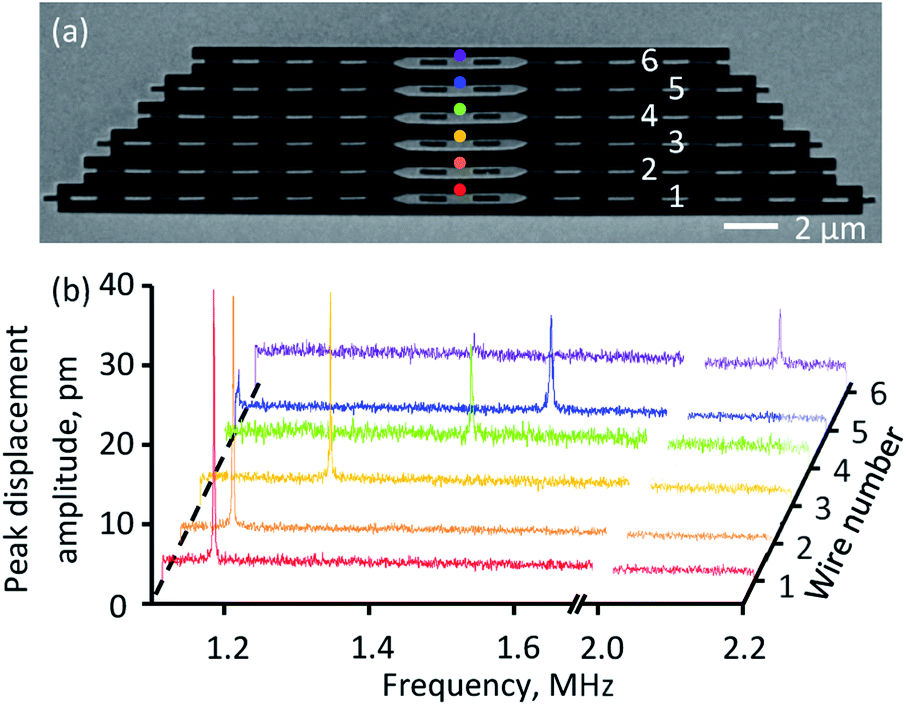 | ||
| Fig. 2 Detecting thermal (Brownian) motion in nanostructures. (a) Static secondary electron image of an array of six free-standing, gold-coated silicon nitride nanowires with lengths between 20 and 30 μm. (b) Frequency dispersion of the nanowires' thermal [Brownian] motion displacement amplitude measured with the incident electron beam focused at the points denoted by colored dots in (a). Peaks correspond to the [length-dependent] fundamental in-plane oscillatory resonant frequencies. | ||
From experimental data, RMS displacement amplitude can be evaluated as 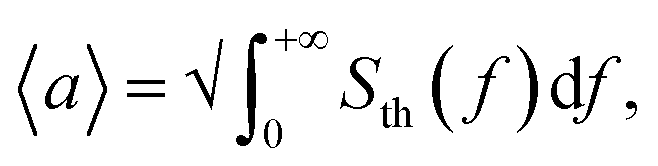 where Sth(f) is the power spectral density (PSD) of displacement,18 which in turn is obtained as the square of the displacement data plotted in Fig. 2b divided by instrumental bandwidth. The area under the PSD curve gives the variance of displacement 〈a2〉. RMS displacement amplitudes of the six beams in the experimental sample are (in descending order of their lengths) 156, 152, 144, 132, 124 and 94 pm, i.e., a small fraction of silicon–nitrides' 0.76 nm (β phase) crystal lattice parameter.19 (We note here that the effect of electron beam-induced heating amounts to an estimated local temperature increase of only ∼1 K at the centre of a nanowire. With RMS displacement being proportional to the square root of temperature, this translates to a negligible perturbation of <0.25 pm against the measured ≳100 pm RMS nanowire displacements.)
Application of the motion detection technique to the spatial mapping of externally driven movements is illustrated in Fig. 3. For this purpose, samples are mounted on a piezoelectric actuator and the incident electron beam is raster-scanned over the sample, with the amplitude and phase of the secondary electron current oscillation detected at the piezo driving frequency by a lock-in amplifier. The point-by-point raster, with an integration time of 20 μs at each pixel (and as above a 5 kV, 86 pA electron beam), is externally triggered for consistent registration of phase over the entire image area. Fig. 3, referencing Robert Hooke's iconic 1665 optical microscopic image,20 shows stimulated nano-motion electron microscopic images of a (deceased) flea at a selection of different driving frequencies. The imaged maxillary palpus and coxa region include setae that are a few tens of micrometres long and a few hundred nanometres in diameter, are here found to have natural oscillation frequencies in the sub-MHz range. The images (Fig. 3b–d) reveal resonant oscillatory displacement amplitudes reaching a few hundred nanometres (in response to a piezo actuator in-plane drive amplitude of ∼10 nm and against a background of the whole sample moving with said amplitude – dark blue features in the upper panels of Fig. 3b–d). The lower panels in Fig. 3b–d show the phase of the modulated secondary electron signal relative to the (piezo) driving force. This depends on both the local gradient and the motion mode shape of the structure: the absence of phase discontinuities along the long edges of resonantly oscillating setae show that they are moving in a fundamental flexural mode, i.e. that all points along the length are moving in the same direction at the same time.
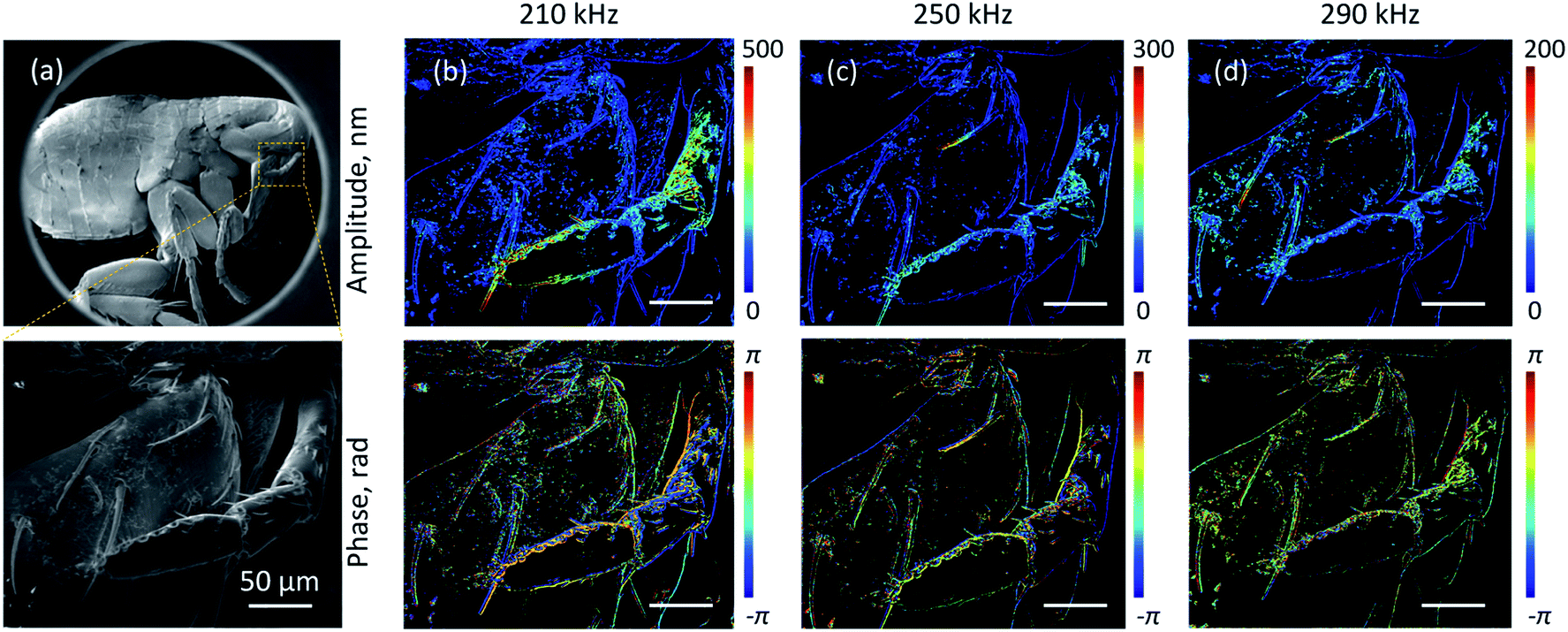 | ||
| Fig. 3 Hyperspectral imaging of driven oscillations of flea setae. (a) Static secondary electron image of the entire flea and enlarged detail of the motion-imaged area. (b–d) Amplitude (upper row) and corresponding phase (lower) of secondary electron signal modulation at selected driving frequencies [as labelled]. | ||
Conclusions
In summary, we have demonstrated that the time-domain analysis of secondary electron emission in electron microscopy can provide for mapping of fast (kHz–MHz) thermal and stimulated movement in nano/microstructures with sub-atomic displacement sensitivity, enabling the detection and hyperspectral spatial mapping of thermal (Brownian) motion, and coherent (externally driven) oscillations. The technique can be applied to a wide variety of artificial and naturally occurring objects, providing quantitative information directly on their vibrational modes, short-timescale ‘ballistic’ motion dynamics,3,4,21 and indirectly on their mass, elasticity and the forces acting upon them.Author contributions
J. Y. O. conceived the idea for the experiment. J. Y. O. and T. L. configured the instrument. T. L. carried out the measurements and manufactured the nanowire sample. All authors discussed the results, analysed the data, and contributed to writing the paper. K. F. M. and N. I. Z. supervised the work.Conflicts of interest
There are no conflicts to declare.Acknowledgements
This work is supported by the UK Engineering and Physical Sciences Research Council (grants EP/M009122/1 and EP/T02643X/1), the Singapore Ministry of Education (NIZ – grant MOE2016-T3-1-006) and the China Scholarship Council (TL – grant 201806160012).References
- N. I. Zheludev and E. Plum, Nat. Nanotechnol., 2016, 11, 16 CrossRef CAS.
- K. Ekinci and M. Roukes, Rev. Sci. Instrum., 2005, 76, 061101 CrossRef.
- T. Li, S. Kheifets, D. Medellin and M. G. Raizen, Science, 2010, 328, 1673–1675 CrossRef CAS.
- S. Kheifets, A. Simha, K. Melin, T. Li and M. G. Raizen, Science, 2014, 343, 1493–1496 CrossRef CAS.
- M. Roukes, Phys. World, 2001, 14, 25 CrossRef CAS.
- L. Midolo, A. Schliesser and A. Fiore, Nat. Nanotechnol., 2018, 13, 11–18 CrossRef CAS.
- X. Zhao, G. Duan, A. Li, C. Chen and X. Zhang, Microsyst. Nanoeng., 2019, 5, 1–17 CrossRef CAS.
- A. Karvounis, B. Gholipour, K. F. MacDonald and N. I. Zheludev, Adv. Mater., 2019, 31, 1804801 CrossRef.
- A. Karvounis, N. Aspiotis, I. Zeimpekis, J. Y. Ou, C. C. Huang, D. Hewak and N. I. Zheludev, Adv. Sci., 2019, 6, 1900974 CrossRef CAS.
- A. Bernheim-Groswasser, N. S. Gov, S. A. Safran and S. Tzlil, Adv. Mat., 2018, 30, 1707028 CrossRef.
- L. Woods, D. A. R. Dalvit, A. Tkatchenko, P. Rodriguez-Lopez, A. W. Rodriguez and R. Podgornik, Rev. Mod. Phys., 2016, 88, 045003 CrossRef.
- M. Krieg, G. Fläschner, D. Alsteens, B. M. Gaub, W. H. Roos, G. J. Wuite, H. E. Gaub, C. Gerber, Y. F. Dufrêne and D. J. Müller, Nat. Rev. Phys., 2019, 1, 41–57 CrossRef.
- F. Xia and L. Jiang, Adv. Mater., 2008, 20, 2842–2858 CrossRef CAS.
- S. Wang, Z. Shan and H. Huang, Adv. Sci., 2017, 4, 1600332 CrossRef.
- J. I. Goldstein, et al., Scanning electron microscopy and X-ray microanalysis, Springer International Publishing, 4th edn, 2017 Search PubMed.
- B. Averill and P. Eldredge, General chemistry: principles, patterns, and applications, 2011 Search PubMed.
- B. D. Hauer, C. Doolin, K. S. D. Beach and J. P. Davis, Ann. Phys., 2013, 339, 181–207 CAS.
- M. Aspelmeyer, T. J. Kippenberg and F. Marquardt, Rev. Mod. Phys., 2014, 86, 1391 CrossRef.
- D. Du Boulay, et al. , Acta Crystallogr., Sect. B: Struct. Sci., Cryst. Eng. Mater., 2004, 60, 388–405 CrossRef CAS.
- R. Hooke, Micrographia: or some physiological descriptions of minute bodies made by magnifying glasses, with observations and inquiries thereupon, The Royal Society, 1665 Search PubMed.
- Y. Shi, S. Xiong, L. K. Chin, J. Zhang, W. Ser, J. Wu, T. Chen, Z. Yang, Y. Hao, B. Liedberg, P. H. Yap, D. P. Tsai, C. W. Qiu and A. Q. Liu, Sci. Adv., 2018, 4, eaao0773 CrossRef.
Footnote |
| † Following a period of embargo, the data from this paper can be obtained from the University of Southampton ePrints research repository: https://doi.org/10.5258/SOTON/D1742 |
| This journal is © The Royal Society of Chemistry 2021 |