
 Open Access Article
 This Open Access Article is licensed under a Creative Commons Attribution-Non Commercial 3.0 Unported Licence
Ambient processed (110) preferred MAPbI3 thin films for highly efficient perovskite solar cells
Rui
Guo
 a,
Biplav
Dahal
a,
Arun
Thapa
a,
Yuba Raj
Poudel
a,
Yunyan
Liu
b and
Wenzhi
Li
*a
a,
Biplav
Dahal
a,
Arun
Thapa
a,
Yuba Raj
Poudel
a,
Yunyan
Liu
b and
Wenzhi
Li
*a
aDepartment of Physics, Florida International University, Miami, FL 33199, USA. E-mail: Wenzhi.Li@fiu.edu
bSchool of Physics and Optoelectronic Engineering, Shandong University of Technology, Zibo, Shandong 255049, P. R. China
First published on 5th February 2021
Abstract
Organic–inorganic hybrid perovskites have attracted intensive attention due to their exceptional optoelectronic properties. With a massive leap of efficiency from 3.8% to 25.2% in a decade, perovskite solar cells (PSCs) have been considered the most promising next-generation photovoltaic technology. Recently, the methylamine (MA)-gas-mediated approach has been widely studied for preparing precursor solutions to deposit large scale perovskite thin films for PSCs. In this article, high-quality MAPbI3 films were spin-coated using a MA-gas-mediated perovskite precursor. The deposited MAPbI3 films showed larger crystal grains, lower surface roughness, and a preferred (110) crystal orientation compared to the films deposited by the Lewis adduct method. Planar PSC devices fabricated using the MA-gas-mediated precursor showed a high efficiency of 19.28% and a higher average efficiency than the devices fabricated by the Lewis adduct method.
Introduction
Organic–inorganic hybrid perovskite solar cells (PSCs) have attracted immense attention in the field of emerging photovoltaics (PVs) in the last decade.1–5 Since the first application of methylammonium lead iodide (CH3NH3PbI3 or MAPbI3) as the light-absorbing nanoparticles in dye-sensitized solar cells in 2009,6 the certified power conversion efficiencies (PCEs) of single-junction PSCs, recorded in the best research-cell efficiency chart provided by the National Renewable Energy Laboratory, have achieved a massive leap from 3.8% to 25.2%,7 rivaling mainstream multi-crystalline silicon solar cells. Such an unprecedented PCE advancement is the fastest among all the next-generation photovoltaic devices, which is highly attributed to the optimization of the composition of perovskites,8–14 improved crystal growth control,15–22 as well as interface23–26 and device engineering.27–32 As a result of their many preferred characteristics, including low-cost fabrication process, high absorption coefficient in the visible range,1,33 high charge carrier mobility,34,35 long diffusion length,14,36,37 and tunable direct bandgap,38,39 PSCs have been viewed as the leading candidates for the next-generation PV technologies.On top of the preeminently high PCE among various next-generation PV technologies, the ease of processing, with which high-quality organic–inorganic hybrid perovskites thin films can be deposited,40 is another characteristic that makes these materials extremely attractive for solar cell devices. Although various methods have been developed to deposit perovskite films,40,41 one-step spin coating remains the easiest and quickest route to depositing high-quality perovskite layers. The choice of available solvents is limited due to the low solubility of PbI2 in most common nonpolar solvents or polar protic solvents. The most common solvents used in one-step spin coating are dimethylformamide (DMF),16,42 dimethyl sulfoxide (DMSO),43–45 and γ-butyrolactone (GBL),46 all of which are polar aprotic solvents with relatively high boiling temperatures (>100 °C). During spin coating, these polar aprotic solvents are generally removed by the centrifugal force. An anti-solvent dripping process is usually required for a dense and pinhole-free thin film.42,46,47 The as-spun thin film is usually in an intermediate phase formed by the complex or adduct of the perovskite solute and the solvent molecules.16,43 In the annealing process, the solvent molecules are evaporated by heat, converting the intermediate phase to perovskite crystals. Therefore, the physical properties of the solvents are critical for perovskite crystallization.
However, the one-step spin coating method with anti-solvent dripping is not applicable for coating large-area perovskite thin films. Recently, many alternative methods have been developed for coating large-area perovskite thin films, including blade,48 D-bar,5 slot-die,49 and spray coating,50 stamping,45 and pressure process.51 One common point shared by some of these methods is preparing the perovskite precursor solution through a methylamine (MA) gas-mediated solid–liquid transition. Such an effect was first reported in a MA-gas-induced defect healing technique in 2015.52 A solid perovskite film can be quickly converted to a liquid phase in the presence of MA gas. The liquid phase can return to the solid perovskite phase with a better crystalline quality once the MA gas atmosphere is removed. This technique has been applied to prepare perovskite precursor solutions to fabricate large-scale PSCs.5,53 Here, we demonstrate the preparation of a MA-gas-mediated MAPbI3 precursor solution in the ambient environment (25 °C, 50% relative humidity). High-quality spin-coated MAPbI3 thin films showed a preferred (110) orientation in the crystal structure and larger crystal grains than the MAPbI3 films deposited by the Lewis adduct method.44 Planar PSCs with a configuration of FTO/SnO2/MAPbI3/spiro-OMeTAD/Au were fabricated using MAPbI3 films deposited using the MA-gas-mediated precursor and the Lewis adduct precursor. The PSC devices using the MA-gas-mediated precursor exhibited superior performance to the devices using the Lewis adduct method and achieved a maximum PCE of 19.28%.
Experimental details
Preparation of the MAPbI3·MAx precursor
The MAPbI3·MAx precursor solution in acetonitrile was prepared in an ambient environment. Typically, 190.8 mg methylammonium iodide (1.2 mmol of MAI, Lumtec) and 553.2 mg lead iodide (1.2 mmol of PbI2, beads, 99.999% trace metals basis, perovskite grade, Sigma-Aldrich) were mixed in 2 mL anhydrous acetonitrile (ACROS Organic) and stirred for 30 min to form a black mixture comprising MAPbI3 and unreacted PbI2 and MAI. To produce MA gas, Ar was bubbled at a flow rate of 40 sccm into a methylamine (MA) solution in ethanol (Sigma-Aldrich, 33 wt%) maintained at 0 °C using an ice bath. The produced MA gas was passed through drying tubes filled with drierite and calcium oxide powder, and then bubbled directly into the black mixture until the black mixture became a clear, transparent, light-yellow solution. Then, the clear solution was filtered through a PTFE syringe filter with a pore size of 0.2 um to remove any big particles and stored in a sealed vial for later use.Preparation of the MAPbI3·DMSO precursor
The recipe for the MAPbI3·DMSO precursor was based on the Lewis adduct method published by Park et al.16 Typically, 159 mg MAI (Lumtec) and 461 mg PbI2 (99.999% trace metals basis, perovskite grade, Sigma-Aldrich) were mixed in 633 μL N,N-dimethylformamide (DMF, anhydrous, 99.8%, Alfa Aesar) and 70.8 μL dimethyl sulfoxide (DMSO, anhydrous, ≥99.9%, Sigma-Aldrich) inside a N2-filled glovebox. The mixture was stirred for 2 hours to obtain a clear, light yellow solution.Deposition of MAPbI3 thin films
MAPbI3 thin films were spin coated by two different procedures depending on the precursor solution used.(a) For the MAPbI3·MAx precursor, 50 μL precursor solution was cast onto the substrate and spin coated at 2000 rpm for 35 s with a ramp of 1000 rpm per second in the ambient environment. Immediately after spin coating, a uniform, dense, and mirror-like brown perovskite thin film was deposited, and it was annealed on a hot plate at 90 °C for 5 min. During the annealing process, the substrate was covered with a glass Petri dish, and dried MA/Ar gas was passed into the Petri dish. The MAPbI3 thin film deposited by this method will be referred to as ‘MAPbI3 by MAPbI3·MAx’ in the following sections.
(b) For the MAPbI3·DMSO precursor solution, the spin coating procedure was modified based on the published results.16 Typically, the substrate was treated with oxygen plasma for 10 min and used immediately. 45 μL MAPbI3·DMSO precursor was cast onto the substrate and spin-coated at 4000 rpm with a ramp of 2000 rpm per second in the ambient environment. After the substrate was spun at 4000 rpm for 10 s, 900 μL diethyl ether was gently and continuously cast onto the substrate within 2 s. Then, the spinning substrate was stopped immediately, and a transparent, light green film was formed on top of the substrate. The substrate was then baked on a hot plate at 65 °C for 1 min and 90 °C for 2 min. During the annealing process, the color of the deposited film quickly changed from light green to brown color after annealing at 65 °C and then to a dark brown color after annealing at 90 °C. The MAPbI3 thin film deposited by this method will be referred to as ‘MAPbI3 by Lewis adduct’ in the following sections.
PSC fabrication
Pre-patterned glass/FTO substrates (TEC-15) were obtained from Suzhou Solarflex Optoelectronic Technology Co., LTD. The sheet resistance of the substrate is less than 15 ohms per square, and the thicknesses of the glass substrate and the FTO coating are 2.2 mm and 350 nm, respectively. The average transmittance of glass/FTO in the visible light region is above 80%. The glass/FTO substrate was sequentially cleaned by ultra-sonication with detergent, deionized water, acetone, and ethanol for 15 min each. The clean glass/FTO substrate was dried and treated in oxygen plasma (Harrick Plasma, PDC-32G) for 15 min immediately before depositing the SnO2 electron transporting layer. The SnO2 colloid precursor (tin(IV) oxide, 15 wt% in H2O colloidal dispersion, Alfa Aesar) was diluted with deionized H2O (Thermo Scientific™ reagent grade deionized water) to 8 wt% before use. The diluted SnO2 precursor solution was spin coated onto a glass/FTO substrate at 2000 rpm for 30 s. The substrate was then dried on a hot plate at 80 °C for 10 min and annealed in ambient air at 165 °C for 30 min. After the substrate was allowed to cool down to room temperature, the MAPbI3 thin film was deposited by the spin coating methods as described above. The precursor solution of the hole transporting layer (HTL) was prepared inside a N2-filled glovebox by dissolving 72.3 mg of 2,2′,7,7′-tetrakis(N,N-di-p-methoxyphenylamine)-9,9′-spirobifluorene (spiro-OMeTAD), 28.8 μL of 4-tert-butylpyridine (Aldrich, 96%), and 17.5 μL of lithium bis (trifluoromethanesulfonyl) imide (Li-TFSI, Aldrich, 99.95%) solution (520 mg Li-TSFI in 1 mL anhydrous acetonitrile) in 1 mL of anhydrous chlorobenzene (ACROS). The HTL was deposited on top of the perovskite film by spin coating 55 μL precursor solution at 4000 rpm for 40 s in the ambient environment. The sample was stored overnight inside a desiccator with a relative humidity of 15% or less for oxygen doping. Finally, a 150 nm-thick gold counter electrode was deposited using an e-beam evaporator at a vacuum pressure of 3 × 10⁻⁶ torr. The area of each solar cell device is 0.12 cm2.Characterization
The morphology of the perovskite thin film and the cross-section of the assembled device were observed using a field emission scanning electron microscope (FE-SEM, JEOL 6335F). An atomic force microscope (AFM) in tapping mode (Veeco Multimode Nanoscope III D) was used to characterize the surface morphology and the height profile of the perovskite thin film. Optical absorption properties were characterized using a UV-Vis spectrometer (Agilent Cary 5000 UV-Vis-NIR spectrometer). Crystal structure analysis of the perovskite films was carried out using an X-ray diffractometer (Siemens D5000) with a Cu Kα source (λ = 1.5406 Å) at room temperature. The J–V curve of the solar cell was measured using a source meter (Keithley 2400) under AM 1.5G illumination from a solar simulator (Newport).Results and discussion
The schematic illustration of the experimental setup to dissolve the black mixture in acetonitrile using MA gas is shown in Fig. 1(A). PbI2 and MAPbI3 have low solubility in acetonitrile at room temperature. As MA gas was being introduced and dissolved in acetonitrile, MAPbI3 gradually dissolved, revealing unreacted yellow cores of PbI2, which indicates the incomplete reaction between PbI2 and MAI. Instead of being converted to perovskite first, the yellow PbI2 core dissolved directly with the help of MA gas, which is in line with earlier reports that the CH3NH2 molecule could interact with PbI2 crystals.51 When all solid materials were dissolved, the final product was a clear light-yellow solution, as shown in Fig. 1(B). The reaction between PbI2 and MA in the presence of moisture would result in the formation of PbO and Pb(OH)2 [eqn (1.1)–(1.3)]. Therefore, it is vital to ensure that the entire setup is tightly sealed and adequately purged to minimize the influence of moisture. Otherwise, moisture would lead to the formation of white PbO and Pb(OH)2 precipitate in a light-yellow solution as shown in Fig. 1(C). Fig. 1(D) and (E) show the diagrams of the deposition procedures using the MAPbI3·DMSO Lewis adduct precursor and the MAPbI3·MAx precursor, respectively. For the MAPbI3·DMSO Lewis adduct precursor, the anti-solvent quenching process is crucial for depositing a dense and pin-hole free MAPbI3 thin film. The as-spun thin film is in the MAPbI3·DMSOx intermediate phase rather than in the MAPbI3 perovskite phase. When the as-spun thin film was heated (65 °C for 1 min and 90 °C for 2 min), DMSO molecules evaporated, and the intermediate phase was converted to the perovskite phase. The spin coating procedure for the MAPbI3·MAx precursor is much simpler as it does not require the anti-solvent quenching process. Therefore, the MAPbI3·MAx precursor is more suitable for depositing large scale perovskite thin films than the MAPbI3·DMSO precursor. During spin coating, MA molecules were removed by evaporation, and MAPbI3 crystals were deposited on top of the substrate forming the as-spun thin film.| 3PbI2 + 2CH3NH2 + H2O → 2CH3NH3PbI3 + PbO↓ | (1.1) |
| CH3NH2 + H2O → CH3NH3OH | (1.2) |
| 3PbI2 + 2CH3NH3OH → 2CH3NH3PbI3 + Pb(OH)2↓ | (1.3) |
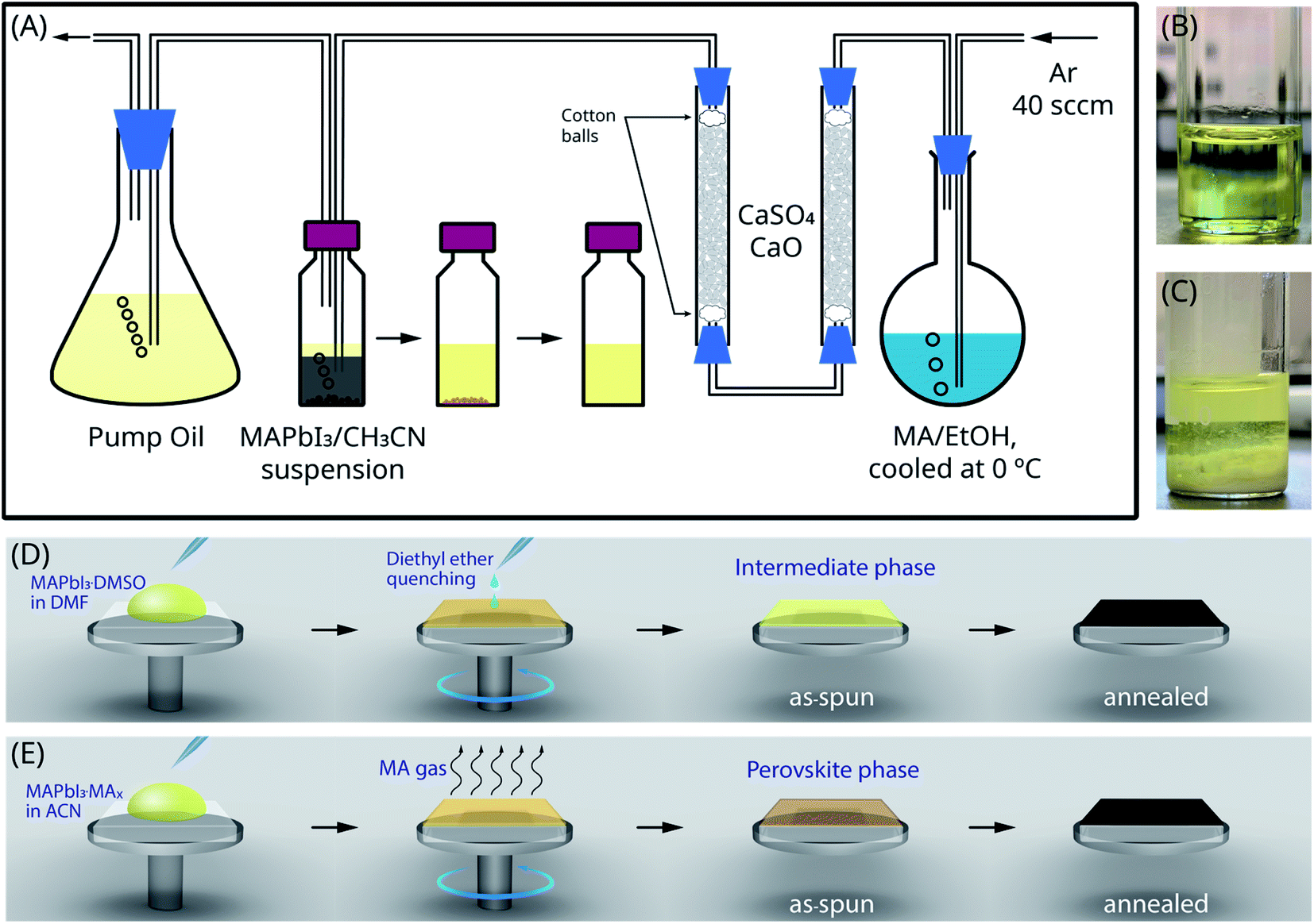 | ||
| Fig. 1 (A) Schematic illustration of the experimental setup to prepare the MAPbI3·MAx precursor solution. (B) and (C) Images of the MAPbI3·MAx solutions prepared with and without moisture, respectively. (D) and (E) Diagrams of the deposition procedures using the MAPbI3·DMSO and the MAPbI3·MAx precursor solutions, respectively. | ||
The surface morphology of the MAPbI3 thin films was characterized using SEM and AFM, as shown in Fig. 2(A)–(F). Both the SEM and AFM topography images indicate the formation of highly crystalline, dense, and pinhole-free MAPbI3 thin films deposited by both methods. The 3D AFM views imply that the MAPbI3 thin film deposited using the MAPbI3·MAx precursor solution [Fig. 2(F)] has a smaller surface roughness than that deposited using the Lewis adduct precursor solution [Fig. 2(E)]. The root mean square (RMS) roughness (Rq) was calculated for both samples. The MAPbI3 by Lewis adduct had an Rq of 16.6 nm, while the MAPbI3 by MAPbI3·MAx had an Rq of 12.7 nm. The smoothness of the perovskite layer has an impact on the quality of the spiro-OMeTAD layer spin coated on top of it. A smoother top surface of the MAPbI3 layer leads to a uniform spiro-OMeTAD layer with better quality and fewer pinholes, which could improve the power conversion efficiency. The diameters of the crystal grains were measured as the maximum horizontal sizes of the crystal grains in the SEM images and displayed as histograms in Fig. 2(G) and (H). The histograms were fitted to the Gamma distribution model, shown as the solid blue and red curves in Fig. 2(G) and (H), respectively. Both the histograms and the distribution curves reveal that the MAPbI3 film prepared using the MAPbI3·MAx precursor has larger crystal grains than that prepared using the Lewis-adduct precursor. The average diameter of the crystal grains in the MAPbI3 film prepared using the MAPbI3·MAx precursor was 433 nm, whereas the average diameter of the crystal grains in the MAPbI3 film prepared using the Lewis-adduct precursor was only 221 nm. Fig. 2(I) shows the optical absorption spectra of the MAPbI3 thin films deposited using the two precursors. Both samples showed high absorbance in the visible wavelength range with clear absorption onsets at about 780 nm. The slight absorbance difference across the range of 400 to 750 nm between the two samples was likely attributed to the difference in thin film thicknesses. The MAPbI3 thin film deposited using MAPbI3·MAx showed less absorption in the range beyond the absorption onset than the MAPbI3 thin film deposited using the Lewis adduct, which is in line with the surface roughness measured by AFM.
 | ||
| Fig. 2 SEM images of MAPbI3 by Lewis adduct (A) and MAPbI3 by MAPbI3·MAx (B). AFM topography images of MAPbI3 by Lewis adduct (C) and MAPbI3 by MAPbI3·MAx (D) and the corresponding 3D views are shown in (E) and (F). Diameter distribution of crystal grains measured in the AFM images of MAPbI3 by Lewis adduct (G) and MAPbI3 by MAPbI3·MAx (H). (I) Optical absorption spectra of MAPbI3 by Lewis adduct and MAPbI3 by MAPbI3·MAx. | ||
Crystal structure analysis of the perovskite thin films deposited on top of SnO2-coated FTO substrates by both methods was carried out by X-ray diffraction (XRD). The absolute intensity (area) of each peak is calculated by integration. To get the relative intensity of each XRD peak, its absolute intensity is divided by the absolute intensity of the most intense peak, i.e., I/I0. The XRD pattern of the MAPbI3 by Lewis adduct is shown in Fig. 3(A). The positions of the peaks were measured and checked with previous reports46,54 to label each peak with the corresponding Miller index, which specified a tetragonal (I4/mcm) crystal structure for the MAPbI3 thin film deposited by the Lewis adduct precursor. Multiple peaks, including (110), (114), (321), (312), and (121), were observed, suggesting that the MAPbI3 thin film deposited by the Lewis adduct method did not feature a preferred orientation. To study the crystal structures of the MAPbI3 thin films deposited using the MAPbI3·MAx precursor solution, XRD spectra of the as-spun MAPbI3 thin film, the MAPbI3 thin film baked in air, and the MAPbI3 thin film baked in air with MA gas were recorded and are displayed in Fig. 3(B)–(D), respectively. All three MAPbI3 thin films exhibited the same tetragonal phase structure as the MAPbI3 thin film deposited by the Lewis adduct method. Comparing the relative intensities of XRD peaks in Fig. 3(B)–(D), the MAPbI3 thin films deposited using the MAPbI3·MAx precursor solution showed significantly stronger (110) and (220) peaks over other peaks that are not parallel to the {110} planes even before annealing.
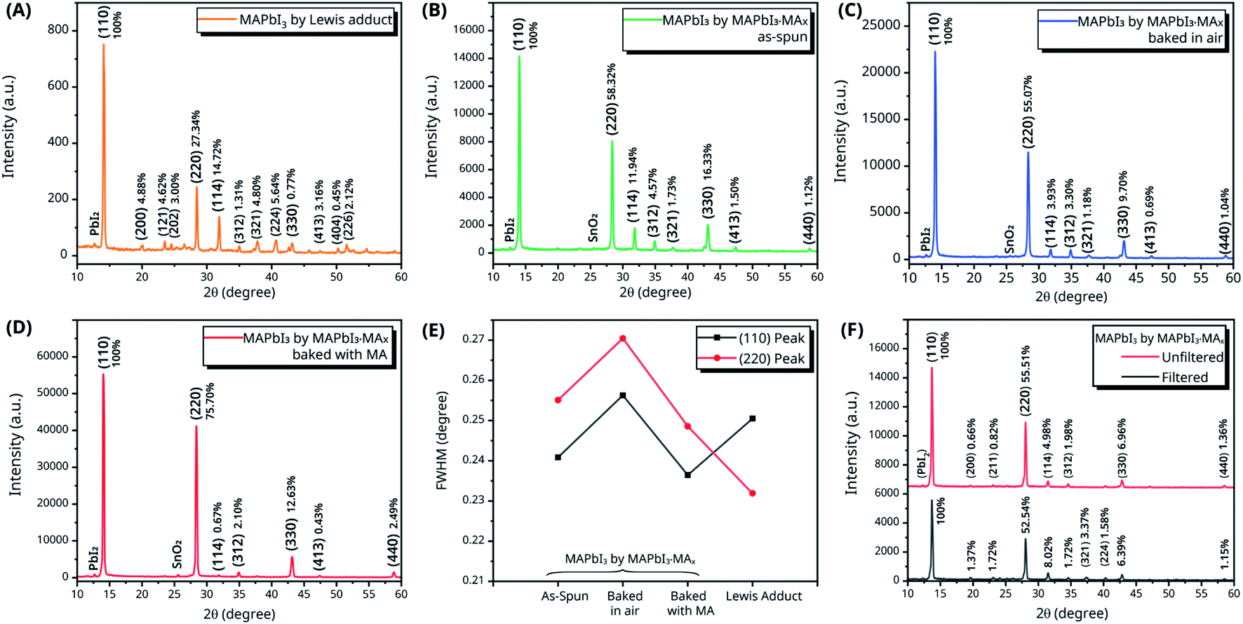 | ||
| Fig. 3 XRD spectra with relative intensity of (A) MAPbI3 by Lewis adduct, (B) as-spun MAPbI3 by MAPbI3·MAx, (C) MAPbI3 by MAPbI3·MAx baked in air, and (D) MAPbI3 by MAPbI3·MAx baked in air with MA gas. (E) Full widths at half maximum (FWHMs) of the (110) peak (solid red line) and (220) peak (solid black line). (F) XRD spectra of the MAPbI3 thin film deposited using filtered and unfiltered MAPbI3·MAx precursor solutions. | ||
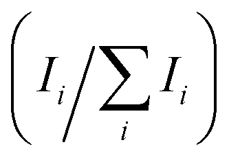
For further comparison, the ratios of the XRD intensities for the {110} planes vs. the sum of intensities of all XRD peaks are calculated and displayed in Table 1. The last row in Table 1 represents the ratio of the sum of intensities of XRD peaks for planes that are not parallel to the {110} planes vs. the sum of intensities of all peaks. The intensity ratios of XRD peaks demonstrated the dominant role of the XRD peaks for the {110} planes over other crystal plane orientations in the MAPbI3 thin films deposited using the MAPbI3·MAx precursor, which was not seen in the MAPbI3 thin films deposited using the Lewis adduct precursor solution. In addition, the annealing process could further reduce the intensity ratio of XRD peaks for planes that are not parallel to the {110} planes, indicating an enhancement in the preferred crystal orientation. The full widths at half maximum (FWHMs) of the (110) and (220) peaks in Fig. 3(A)–(D) were measured and are plotted in Fig. 3(E). The comparison between the FWHMs of the (110) and (220) peaks of the three MAPbI3 thin films deposited using the MAPbI3·MAx precursor indicates that the MA gas helps to reduce the FWHMs of the (110) and (220) peaks and therefore increase the crystallinity of the MAPbI3 thin films. Compared with the FWHM of the (110) peak of the MAPbI3 thin film deposited by the Lewis adduct method, the FWHM of the (110) peak of the MAPbI3 thin film deposited using MAPbI3·MAx and annealed in the MA gas atmosphere is smaller. It is clear that the MAPbI3 thin film deposited using the MAPbI3·MAx precursor solution exhibited higher crystallinity and a preferred crystal orientation in the 〈110〉 direction, which is similar to the result in defected MAPbI3 thin films healed by MA gas treatment.52,55,56
 in Fig. 3(A)–(D)
| (hkl) | Intensity ratio
|
|||
|---|---|---|---|---|
| MAPbI3 by Lewis adduct | MAPbI3 by MAPbI3·MAx | |||
| As-spun | Baked in air | Baked in MA | ||
| (110) | 57.86 | 51.15 | 57.18 | 51.54 |
| (220) | 15.81 | 29.83 | 31.49 | 39.02 |
| (330) | 0.44 | 8.35 | 5.54 | 6.51 |
| (440) | 0.00 | 0.57 | 0.59 | 1.29 |
| Other | 25.89 | 10.09 | 5.20 | 1.65 |

The XRD spectra of the MAPbI3 films deposited using filtered (using a PTFE syringe filter with a pore size of 0.2 μm) and unfiltered MAPbI3·MAx precursor solutions were measured and are shown in Fig. 3(F). The XRD patterns depict that MAPbI3 deposited using the unfiltered MAPbI3·MAx precursor showed stronger and sharper (110) and (220) peaks, and hence there is stronger crystal orientation preference in the 〈110〉 direction. Park et al.5 suggested that cluster-like MAPbI3 nanocrystals (NCs) existed in the MAPbI3·MAx precursor solution. The unfiltered MAPbI3·MAx precursor contained more MAPbI3 NCs, especially larger MAPbI3 NCs. Acting as the seed crystals, these NCs played a crucial role in initiating and facilitating MAPbI3 nucleation during the spin coating process. It is highly likely that the orientations of such MAPbI3 NCs at the beginning of the nucleation process determine the crystal orientations in the deposited perovskite thin films. Therefore, one can assume that, at the beginning of nucleation, the MAPbI3 NCs feature the same preferred orientation in the 〈110〉 direction. However, current experimental results are not sufficient to draw a solid conclusion on the mechanism for the preferred orientation, and more experiments are needed to investigate it further.
The cross-sectional SEM image of the assembled PSC device using the filtered MAPbI3·MAx precursor solution and the schematic of the device are shown in Fig. 4(A). The cross-sectional SEM image clearly shows a MAPbI3 layer of about 370 nm thickness, which is between the spiro-OMeTAD and SnO2 layers. In the conventional n-i-p planar PSCs, TiO2 is used as the electron transporting material (ETM). In our device, a thin layer of SnO2 is deposited as the ETM as it has a better energy band alignment with MAPbI3 and higher electron conductivity than TiO2. Fig. 4(B) shows the J–V curves of the PSC devices fabricated using the Lewis adduct precursor and the MAPbI3·MAx precursor. It is clear that the PSC device fabricated using the MAPbI3·MAx precursor has higher VOC and JSC than the PSC device fabricated using the Lewis adduct precursor. The highest PCE of the PSC device fabricated using the MAPbI3·MAx precursor was observed in the reverse scan, providing VOC = 1.073 V, JSC = 24.169 mA cm−2, FF = 74.37%, and PCE = 19.28%, and the J–V curve is shown as the solid black line in Fig. 4(B). The PSC device fabricated using the Lewis adduct precursor showed VOC = 1.020 V, JSC = 23.421 mA cm−2, FF = 76.09%, and PCE = 18.17%, and the J–V curve is shown as the dashed black line in Fig. 4(B). For both devices, the hysteresis effect was observed between the forward- and reverse-scan J–V curves, with smaller VOC and JSC for the forward scan. For a statistical perspective, a comparison of the PCEs of a total of 64 PSC devices fabricated side-by-side using the Lewis adduct precursor and the MAPbI3·MAx precursor was conducted. Fig. 4(C) shows the histogram and Gaussian fitting of the PCEs of 32 PSC devices fabricated using the Lewis adduct precursor. Fig. 4(D) shows the histogram and Weibull fitting of the PCEs of 32 PSC devices fabricated using MAPbI3·MAx. The statistical result showed clearly that PSC devices fabricated using the MAPbI3·MAx precursor have a higher average PCE and a smaller deviation (16.28 ± 2.38%) than those fabricated using the Lewis adduct precursor (12.59 ± 4.01%). After measuring 320 PSC devices fabricated using the MAPbI3·MAx precursor, the histogram of the PCEs of these devices is displayed in Fig. 4(E) and fitted to a Weibull distribution model. The average PCE of all 320 devices fabricated using the MAPbI3·MAx precursor was 14.08 ± 2.73%.
 | ||
| Fig. 4 (A) Cross-sectional SEM image and schematic illustration of the PSC device structure. For clarity, Au, spiro-OMeTAD, and MAPbI3 layers are labeled with gold, green, and red colors, respectively. The small inset on the bottom right corner is the original SEM image of the PSC device. (B) Forward- and reverse-scan J–V curves of the PSCs made using the Lewis adduct precursor and the MAPbI3·MAx precursor. (C) and (D) Histograms and distribution curves of the PCEs of the devices made using the Lewis adduct precursor and the MAPbI3·MAx precursor. (E) Histogram of PCEs of 320 PSC devices fabricated using the MAPbI3·MAx precursor. | ||
Conclusions
In summary, the preparation of the MA-gas-mediated MAPbI3·MAx precursor solution has been demonstrated in the ambient environment. High-quality spin-coated MAPbI3 thin films using the MAPbI3·MAx precursor were deposited with high reproducibility. Compared to films deposited using the Lewis adduct method, the perovskite films deposited using the MAPbI3·MAx precursor showed smooth surfaces, large crystal grains, and a preferred crystal orientation in the 〈110〉 direction. The preferred crystal orientation was further enhanced by annealing the as-deposited films in a MA gas atmosphere. Planar PSCs with a configuration of FTO/SnO2/MAPbI3/spiro-OMeTAD/Au have been fabricated using both the MAPbI3·MAx precursor and the Lewis adduct precursor. The PSC devices made using the MAPbI3·MAx precursor exhibited superior performance compared to the devices made using the Lewis adduct method. Comparing the two types of PSC devices fabricated in the same batch, the average PCEs of the devices fabricated using the MAPbI3·MAx precursor and the Lewis adduct precursor were 16.28% vs. 12.59%, respectively. The maximum PCE of the PSCs made using the MAPbI3·MAx precursor was 19.28%.Author contributions
Rui Guo: conceptualization, methodology, formal analysis, investigation, writing – original draft, writing – review & editing. Biplav Dahal: methodology, formal analysis, investigation, discussion. Arun Thapa: methodology, formal analysis, investigation, discussion. Yuba Raj Poudel: methodology, formal analysis, investigation, discussion. Yunyan Liu: methodology, formal analysis, investigation, discussion. Wenzhi Li: conceptualization, investigation, formal analysis, discussion, writing – review & editing, supervision, funding acquisition, resources.Conflicts of interest
The authors declare no conflict of interest.Acknowledgements
This work is supported by the National Science Foundation under grant DMR-1506640. The authors would also like to acknowledge the support from the Advanced Materials Engineering Research Institute (AMERI) at Florida International University.Notes and references
- H. S. Kim, C. R. Lee, J. H. Im, K. B. Lee, T. Moehl, A. Marchioro, S. J. Moon, R. Humphry-Baker, J. H. Yum, J. E. Moser, M. Gratzel and N. G. Park, Sci. Rep., 2012, 2, 591 CrossRef.
- M. M. Lee, J. Teuscher, T. Miyasaka, T. N. Murakami and H. J. Snaith, Science, 2012, 338, 643–647 CrossRef CAS.
- Z. Xiao, Q. Dong, C. Bi, Y. Shao, Y. Yuan and J. Huang, Adv. Mater., 2014, 26, 6503–6509 CrossRef CAS.
- W. S. Yang, J. H. Noh, N. J. Jeon, Y. C. Kim, S. Ryu, J. Seo and S. I. Seok, Science, 2015, 348, 1234–1237 CrossRef CAS.
- D.-N. Jeong, D.-K. Lee, S. Seo, S. Y. Lim, Y. Zhang, H. Shin, H. Cheong and N.-G. Park, ACS Energy Lett., 2019, 4, 1189–1195 CrossRef CAS.
- A. Kojima, K. Teshima, Y. Shirai and T. Miyasaka, J. Am. Chem. Soc., 2009, 131, 6050–6051 CrossRef CAS.
- Best Research-Cell Efficiencies, National Renewable Energy Laboratory, 2020, https://www.nrel.gov/pv/assets/pdfs/best-research-cell-efficiencies.20200803.pdf Search PubMed.
- J. W. Lee, D. J. Seol, A. N. Cho and N. G. Park, Adv. Mater., 2014, 26, 4991–4998 CrossRef CAS.
- N. J. Jeon, J. H. Noh, W. S. Yang, Y. C. Kim, S. Ryu, J. Seo and S. I. Seok, Nature, 2015, 517, 476–480 CrossRef CAS.
- S.-H. Turren-Cruz, A. Hagfeldt and M. Saliba, Science, 2018, 362, 449–453 CrossRef CAS.
- J.-P. Correa-Baena, Y. Luo, T. M. Brenner, J. Snaider, S. Sun, X. Li, M. A. Jensen, N. T. P. Hartono, L. Nienhaus, S. Wieghold, J. R. Poindexter, S. Wang, Y. S. Meng, T. Wang, B. Lai, M. V. Holt, Z. Cai, M. G. Bawendi, L. Huang, T. Buonassisi and D. P. Fenning, Science, 2019, 363, 627–631 CrossRef CAS.
- L. Qiu, S. He, Y. Jiang, D.-Y. Son, L. K. Ono, Z. Liu, T. Kim, T. Bouloumis, S. Kazaoui and Y. Qi, J. Mater. Chem. A, 2019, 7, 6920–6929 RSC.
- E. Parvazian, A. Abdollah-zadeh, M. Dehghani and N. Taghavinia, ACS Appl. Energy Mater., 2019, 2, 6209–6217 CrossRef CAS.
- J. Tong, Z. Song, D. H. Kim, X. Chen, C. Chen, A. F. Palmstrom, P. F. Ndione, M. O. Reese, S. P. Dunfield, O. G. Reid, J. Liu, F. Zhang, S. P. Harvey, Z. Li, S. T. Christensen, G. Teeter, D. Zhao, M. M. Al-Jassim, M. F. A. M. van Hest, M. C. Beard, S. E. Shaheen, J. J. Berry, Y. Yan and K. Zhu, Science, 2019, 364, 475–479 CrossRef CAS.
- J. W. Jung, S. T. Williams and A. K. Y. Jen, RSC Adv., 2014, 4, 62971–62977 RSC.
- N. Ahn, D. Y. Son, I. H. Jang, S. M. Kang, M. Choi and N. G. Park, J. Am. Chem. Soc., 2015, 137, 8696–8699 CrossRef CAS.
- C. Bi, Q. Wang, Y. Shao, Y. Yuan, Z. Xiao and J. Huang, Nat. Commun., 2015, 6, 7747 CrossRef CAS.
- W. Nie, H. Tsai, R. Asadpour, J. C. Blancon, A. J. Neukirch, G. Gupta, J. J. Crochet, M. Chhowalla, S. Tretiak, M. A. Alam, H. L. Wang and A. D. Mohite, Science, 2015, 347, 522–525 CrossRef CAS.
- Y. Rong, Z. Tang, Y. Zhao, X. Zhong, S. Venkatesan, H. Graham, M. Patton, Y. Jing, A. M. Guloy and Y. Yao, Nanoscale, 2015, 7, 10595–10599 RSC.
- J. Xue, R. Wang and Y. Yang, Nat. Rev. Mater., 2020, 5, 809–827 CrossRef CAS.
- B. Yang, O. Dyck, J. Poplawsky, J. Keum, A. Puretzky, S. Das, I. Ivanov, C. Rouleau, G. Duscher, D. Geohegan and K. Xiao, J. Am. Chem. Soc., 2015, 137, 9210–9213 CrossRef CAS.
- W. A. Dunlap-Shohl, Y. Zhou, N. P. Padture and D. B. Mitzi, Chem. Rev., 2019, 119, 3193–3295 CrossRef CAS.
- H. Zhou, Q. Chen, G. Li, S. Luo, T. B. Song, H. S. Duan, Z. Hong, J. You, Y. Liu and Y. Yang, Science, 2014, 345, 542–546 CrossRef CAS.
- Q. Jiang, Y. Zhao, X. Zhang, X. Yang, Y. Chen, Z. Chu, Q. Ye, X. Li, Z. Yin and J. You, Nat. Photonics, 2019, 13, 460–466 CrossRef CAS.
- H. Tan, A. Jain, O. Voznyy, X. Lan, F. P. Garcia de Arquer, J. Z. Fan, R. Quintero-Bermudez, M. Yuan, B. Zhang, Y. Zhao, F. Fan, P. Li, L. N. Quan, Y. Zhao, Z. H. Lu, Z. Yang, S. Hoogland and E. H. Sargent, Science, 2017, 355, 722–726 CrossRef CAS.
- W. Li, W. Zhang, S. Van Reenen, R. J. Sutton, J. Fan, A. A. Haghighirad, M. B. Johnston, L. Wang and H. J. Snaith, Energy Environ. Sci., 2016, 9, 490–498 RSC.
- Y. Shao, Z. Xiao, C. Bi, Y. Yuan and J. Huang, Nat. Commun., 2014, 5, 5784 CrossRef CAS.
- W. Chen, Y. Wu, Y. Yue, J. Liu, W. Zhang, X. Yang, H. Chen, E. Bi, I. Ashraful, M. Gratzel and L. Han, Science, 2015, 350, 944–948 CrossRef CAS.
- Q. Jiang, X. Zhang and J. You, Small, 2018, 14, e1801154 CrossRef.
- M. Yang, D. H. Kim, T. R. Klein, Z. Li, M. O. Reese, B. J. Tremolet de Villers, J. J. Berry, M. F. A. M. van Hest and K. Zhu, ACS Energy Lett., 2018, 3, 322–328 CrossRef CAS.
- P. Cui, D. Wei, J. Ji, H. Huang, E. Jia, S. Dou, T. Wang, W. Wang and M. Li, Nat. Energy, 2019, 4, 150–159 CrossRef CAS.
- E. H. Jung, N. J. Jeon, E. Y. Park, C. S. Moon, T. J. Shin, T.-Y. Yang, J. H. Noh and J. Seo, Nature, 2019, 567, 511–515 CrossRef CAS.
- S. De Wolf, J. Holovsky, S.-J. Moon, P. Löper, B. Niesen, M. Ledinsky, F.-J. Haug, J.-H. Yum and C. Ballif, J. Phys. Chem. Lett., 2014, 5, 1035–1039 CrossRef CAS.
- C. C. Stoumpos, C. D. Malliakas and M. G. Kanatzidis, Inorg. Chem., 2013, 52, 9019–9038 CrossRef CAS.
- W. Rehman, R. L. Milot, G. E. Eperon, C. Wehrenfennig, J. L. Boland, H. J. Snaith, M. B. Johnston and L. M. Herz, Adv. Mater., 2015, 27, 7938–7944 CrossRef CAS.
- G. Xing, N. Mathews, S. Sun, S. S. Lim, Y. M. Lam, M. Gratzel, S. Mhaisalkar and T. C. Sum, Science, 2013, 342, 344–347 CrossRef CAS.
- S. D. Stranks, G. E. Eperon, G. Grancini, C. Menelaou, M. J. Alcocer, T. Leijtens, L. M. Herz, A. Petrozza and H. J. Snaith, Science, 2013, 342, 341–344 CrossRef CAS.
- J. H. Noh, S. H. Im, J. H. Heo, T. N. Mandal and S. I. Seok, Nano Lett., 2013, 13, 1764–1769 CrossRef CAS.
- G. E. Eperon, S. D. Stranks, C. Menelaou, M. B. Johnston, L. M. Herz and H. J. Snaith, Energy Environ. Sci., 2014, 7, 982–988 RSC.
- Z. Li, T. R. Klein, D. H. Kim, M. Yang, J. J. Berry, M. F. A. M. van Hest and K. Zhu, Nat. Rev. Mater., 2018, 3, 18017 CrossRef CAS.
- N.-G. Park and K. Zhu, Nat. Rev. Mater., 2020, 5, 333–350 CrossRef CAS.
- P. Zhao, B. J. Kim, X. Ren, D. G. Lee, G. J. Bang, J. B. Jeon, W. B. Kim and H. S. Jung, Adv. Mater., 2018, 30, 1802763 CrossRef.
- Y. Rong, S. Venkatesan, R. Guo, Y. Wang, J. Bao, W. Li, Z. Fan and Y. Yao, Nanoscale, 2016, 8, 12892–12899 RSC.
- J. W. Lee, H. S. Kim and N. G. Park, Acc. Chem. Res., 2016, 49, 311–319 CrossRef CAS.
- Y. Zhang, S.-G. Kim, D. Lee, H. Shin and N.-G. Park, Energy Environ. Sci., 2019, 12, 308–321 RSC.
- N. J. Jeon, J. H. Noh, Y. C. Kim, W. S. Yang, S. Ryu and S. I. Seok, Nat. Mater., 2014, 13, 897–903 CrossRef CAS.
- S. Paek, P. Schouwink, E. N. Athanasopoulou, K. T. Cho, G. Grancini, Y. Lee, Y. Zhang, F. Stellacci, M. K. Nazeeruddin and P. Gao, Chem. Mater., 2017, 29, 3490–3498 CrossRef CAS.
- Y. Deng, X. Zheng, Y. Bai, Q. Wang, J. Zhao and J. Huang, Nat. Energy, 2018, 3, 560–566 CrossRef CAS.
- J.-E. Kim, Y.-S. Jung, Y.-J. Heo, K. Hwang, T. Qin, D.-Y. Kim and D. Vak, Sol. Energy Mater. Sol. Cells, 2018, 179, 80–86 CrossRef CAS.
- M. Park, W. Cho, G. Lee, S. C. Hong, M.-c. Kim, J. Yoon, N. Ahn and M. Choi, Small, 2019, 15, 1804005 CrossRef.
- H. Chen, F. Ye, W. Tang, J. He, M. Yin, Y. Wang, F. Xie, E. Bi, X. Yang, M. Gratzel and L. Han, Nature, 2017, 550, 92–95 CrossRef CAS.
- Z. Zhou, Z. Wang, Y. Zhou, S. Pang, D. Wang, H. Xu, Z. Liu, N. P. Padture and G. Cui, Angew Chem. Int. Ed. Engl., 2015, 54, 9705–9709 CrossRef CAS.
- N. K. Noel, S. N. Habisreutinger, B. Wenger, M. T. Klug, M. T. Hörantner, M. B. Johnston, R. J. Nicholas, D. T. Moore and H. J. Snaith, Energy Environ. Sci., 2017, 10, 145–152 RSC.
- M. T. Weller, O. J. Weber, P. F. Henry, A. M. Di Pumpo and T. C. Hansen, Chem. Commun., 2015, 51, 4180–4183 RSC.
- S. R. Raga, Y. Jiang, L. K. Ono and Y. Qi, Energy Technol., 2017, 5, 1750–1761 CrossRef CAS.
- J.-a. Yang, T. Qin, L. Xie, K. Liao, T. Li and F. Hao, J. Mater. Chem. C, 2019, 7, 10724–10742 RSC.
| This journal is © The Royal Society of Chemistry 2021 |