
 Open Access Article
 This Open Access Article is licensed under a Creative Commons Attribution-Non Commercial 3.0 Unported Licence
Enhanced optical absorption in conformally grown MoS2 layers on SiO2/Si substrates with SiO2 nanopillars with a height of 50 nm
Hyeji
Choi
a,
Eunah
Kim
a,
Soyeong
Kwon
a,
Jayeong
Kim
 a,
Anh Duc
Nguyen
b,
Seong-Yeon
Lee
c,
Eunji
Ko
a,
Suyeun
Baek
a,
Hyeong-Ho
Park
d,
Yun Chang
Park
e,
Ki-Ju
Yee
c,
Seokhyun
Yoon
a,
Yong Soo
Kim
b and
Dong-Wook
Kim
*a
a,
Anh Duc
Nguyen
b,
Seong-Yeon
Lee
c,
Eunji
Ko
a,
Suyeun
Baek
a,
Hyeong-Ho
Park
d,
Yun Chang
Park
e,
Ki-Ju
Yee
c,
Seokhyun
Yoon
a,
Yong Soo
Kim
b and
Dong-Wook
Kim
*a
aDepartment of Physics, Ewha Womans University, Seoul 03760, Korea. E-mail: dwkim@ewha.ac.kr
bDepartment of Physics and Energy Harvest Storage Research Center, University of Ulsan, Ulsan 44610, Korea
cDepartment of Physics, Chungnam National University, Daejeon 34134, Korea
dNanodevices Laboratory, Korea Advanced Nano Fab Center, Suwon 16229, Korea
eMeasurement and Analysis Division, National Nanofab Center, Daejeon 34141, Korea
First published on 21st December 2020
Abstract
The integration of transition metal dichalcogenide (TMDC) layers on nanostructures has attracted growing attention as a means to improve the physical properties of the ultrathin TMDC materials. In this work, the influence of SiO2 nanopillars (NPs) with a height of 50 nm on the optical characteristics of MoS2 layers is investigated. Using a metal organic chemical vapor deposition technique, a few layers of MoS2 were conformally grown on the NP-patterned SiO2/Si substrates without notable strain. The photoluminescence and Raman intensities of the MoS2 layers on the SiO2 NPs were larger than those observed from a flat SiO2 surface. For 100 nm-SiO2/Si wafers, the 50 nm-NP patterning enabled improved absorption in the MoS2 layers over the whole visible wavelength range. Optical simulations showed that a strong electric-field could be formed at the NP surface, which led to the enhanced absorption in the MoS2 layers. These results suggest a versatile strategy to realize high-efficiency TMDC-based optoelectronic devices.
Introduction
There have been intensive research efforts to use 2D atomically-thin layered transition metal dichalcogenides (TMDCs) for electronic and optoelectronic device applications. New-concept TMDC-based devices are expected, because TMDCs exhibit intriguing physical properties, such as sizable and tunable bandgap energy, high carrier mobility, and mechanical flexibility.1–14 To prepare high quality TMDC samples, SiO2/Si wafers are the most popular substrates for both mechanical exfoliation from the bulk and thin film deposition.1–4 Optical reflectance, Raman, and photoluminescence (PL) measurements have shown that the output signals of the thin TMDC layers strongly depend on the SiO2 thickness.1–4 Such thickness dependence originates from the Fabry–Perot (FP) resonance in the SiO2 thin films under the TMDC layers.1–3 At the FP resonance, the electric field (E-field) intensity of the incident light at the SiO2 surface exhibits local maxima as a function of the wavelength of incident light, which leads to the enhanced optical absorption in the TMDC layers. Considering these interference effects, approximately 300 nm-thick SiO2/Si wafers have been widely used as substrates for TMDC layers.2,3TMDC layers are often integrated on metal thin films or nanostructures for characterization and application purposes.5–7 Metal layers are used as electrodes for charge injection and collection in active device operations as well as transport measurements.5 TMDC/dielectric/metal structures are fabricated to further increase the surface E-field and resulting absorption, where the metal layers act as back-reflectors.6 Moreover, plasmonic metal nanostructures can strongly concentrate light at the surface and tune the spectral response of the TMDC layers.6,7 Thus, the TMDC–metal hybrid nanostructure provides a platform to investigate the rich physics that originates from photon-plasmon-charge coupling.
TMDC–semiconductor and TMDC–dielectric photonic nanostructures have also been fabricated to improve the light–matter interaction in the TMDC layers.8–14 In contrast to the metals, there is no concern about serious ohmic loss of optical energy in non-metallic materials.15 Sub-wavelength-scaled high refractive index nanostructures can tailor the optical response of TMDC layers owing to the visible-range Mie resonance.8–11 However, growth of high quality TMDC layers directly on either metal thin films or semiconductor substrates is very difficult due to the chemical reaction at the TMDC/substrate interface.
Dielectric materials and their nanostructures have advantages of well-established growth techniques. In addition, their nanostructures can tune the optoelectronic properties of the TMDC layers on them through local strain and strongly confined optical modes.11–14 Unidirectional enhanced light emission from TMD layers on dielectric nanopillars has also been demonstrated.13 Conventional dielectric and semiconductor materials (e.g., SiO2 and Si) have the advantages of well-established large-area deposition and fabrication processes.11,12
In many of the reports mentioned above, TMDC layers are suspended over nanostructures. It is well known that the strain can vary the bandgap energy and carrier concentration of the TMDC layers.12–14,16 Thus, local strain states should be carefully examined to understand and control the physical characteristics of the TMDC layers. The samples with suspended region also have stability issues.7 Incident light can raise the sample temperature, which can induce mechanical stress to the TMDC layers owing to the difference in the thermal expansion coefficients.17,18 If the morphology of the suspended region is changed during repeated optical measurements, reproducible data are hard to obtain. Non-strained and conformal growth of the TMDC layers is desirable to clearly reveal the optical benefits of the nanostructures.
In this work, we prepared a few layers of conformally grown MoS2 on SiO2/Si substrates with SiO2 nanopillars (NPs). The SiO2 NP arrays with a height of 50 nm were fabricated on 100 and 320 nm-thick SiO2/Si wafers. Optical reflectance, photoluminescence, and Raman spectra of the MoS2 layers on the NP region were compared with those obtained from a flat SiO2/Si region. Through optical calculations as well as the experimental measurements, we investigated the influence of the SiO2 NPs on the optical characteristics of the MoS2 layers.
Results and discussion
Fig. 1a and b shows a schematic diagram and a scanning electron microscopy image of a square array of SiO2 NPs with a height of 50 nm and a period of 500 nm. The top and bottom diameters of the SiO2 NPs were 250 and 300 nm, respectively. Si wafers with 100 and 320 nm-thick thermally grown SiO2 layers were used to fabricate the NP-patterned substrates (for detailed fabrication processes, see the Experimental section). The total area of the NP array was 500 × 500 μm2, which will be called the ‘NP’ region hereafter. Around the NP region, there was a dry-etched flat region, which will be called ‘Flat’ region (Fig. 1a). The optical characteristics of such flat region will be presented as well as those of the NP region for comparison. | ||
| Fig. 1 (a) A Schematic diagram of the NP-patterned SiO2/Si substrate and (b) scanning electron microscopy image of the NP region. (c) Optical reflectivity spectra of the patterned substrates fabricated with 100 and 320 nm-SiO2/Si wafers. The spectra of the NP regions – NP(100) and NP(320) – and those of the flat regions – flat(100) and flat(320) – from both substrates can be compared, where the numbers in parentheses indicate the thickness of the SiO2 layers of the non-patterned wafers. | ||
Fig. 1c shows the measured optical reflectivity spectra of the NP-patterned substrates prepared with the 100- and 320-SiO2/Si wafers. An optical microscope equipped with a spectrometer was used to characterize the sub-mm-area NP region. It should be noted that the NPs covering only 28% of the surface area of the NP region enabled the antireflection effects for both SiO2/Si wafers. NP region fabricated on the 100 nm-SiO2/Si wafer exhibited a lower reflectivity over the whole measured wavelength range, compared with flat region on an identical wafer. For the 320 nm-SiO2/Si wafer, the overall reflectivity of NP and flat regions in the 320 nm-SiO2/Si wafer is not largely different. The reflectivity of NP region was smaller than that of flat region at the wavelength range from 550 to 750 nm. The clear dependence on the SiO2 thickness suggests that scattering at the surface NP array alone cannot explain the reflectivity spectra. It has been well known that the optical properties of the MoS2 layers strongly depend on the SiO2 layer thickness of planar SiO2/Si wafers.4 It would be interesting to study how the NPs on thin and thick SiO2 layers affect the optical characteristics of the MoS2 layers on the NP arrays.
MoS2 layers were grown on the NP-patterned SiO2/Si substrates using the metal organic chemical vapour deposition technique. The growth conditions for the MoS2 layer can be found in our earlier publications.11,19 The high-resolution transmission electron microscopy image in Fig. 2a shows that a few layers of MoS2 could be grown on the patterned SiO2 surface even on the vertical sidewall of the NPs. Bright lines are clearly seen at the NP surface in the high angle annular dark-field scanning transmission electron micrograph in Fig. 2b, which indicated conformal growth of the MoS2 layers on the NPs. Hereafter, the NP-patterned substrates coated with the MoS2 layers will be denoted as ‘M100’ and ‘M320’ according to the thickness of the SiO2 layers of the non-patterned SiO2/Si wafers. Fig. 2a and b also reveal the presence of MoS2 layers with non-uniform thickness at the limited area. The optical spectra can reveal the characteristics of the large-volume (or, area) portion of the samples, when the samples have inhomogeneity and/or defects. Comparison of NP and flat regions enables us to study how the NPs can influence the optical properties of the MoS2 layers on them.
 | ||
| Fig. 2 (a) High-resolution and (b) high angle annular dark-field scanning transmission electron microscopy images of the conformally grown MoS2 layers on the NP-patterned SiO2/Si substrates. | ||
Fig. 3a and b shows the micro-PL spectra of M100 and M320 measured at the excitation wavelength of 473 nm. From each sample, the spectra were obtained at the MoS2 layers grown on both NP and flat regions, as indicated in Fig. 3a and b. Strong PL peaks appeared at a wavelength of ∼670 nm in all the measured spectra. This peak position corresponds to the direct gap transition of MoS2 monolayers.1–4 In M100, the PL intensity from NP region (IPL-NP) was larger than that from flat region (IPL-flat): the ratio of IPL-NP/IPL-flat was as large as 1.94. In contrast, the difference between IPL-NP and IPL-flat was very small in M320. It should be noted that the PL peak positions from all the measured regions are almost identical. This indicated that no bandgap reduction, which is a characteristic signature of strain, occurred in our MoS2 layers grown on the NPs.11–13
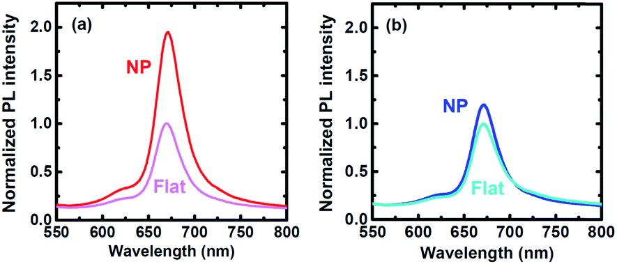 | ||
| Fig. 3 PL spectra of (a) M100 and (b) M320. The spectra from the NP and flat regions are obtained using micron-sized laser beams. The intensity is normalized with respect to the maximum intensity of the flat region for each sample. | ||
Fig. 4a and b shows the Raman spectra of M100 and M320 measured at the wavelength of 532 nm, respectively, where the in-plane (E12g) and out-of-plane (A1g) vibration mode peaks are clearly observed. The Raman peak intensities (IRaman) from NP and flat regions were different. In both M100 and M320, IRaman measured at NP region (IRaman-NP) was larger than that at flat region (IRaman-flat). The ratios of IRaman-NP/IRaman-flat for the A1g peaks were 1.8 and 1.3 for M100 and M320, respectively. IRaman as well as IPL depend on the optical absorption in the sample. Also, it should be noted that the excitation wavelength for the PL measurements (473 nm) was different from that for the PL measurements. Both PL and Raman spectra clearly suggest that the NPs with a height of 50 nm can affect the optical absorption of the few layers of MoS2 on them.
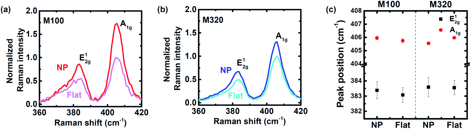 | ||
| Fig. 4 Raman spectra of (a) M100 and (b) M320. The intensity was normalized with respect to the A1g peak intensity of the flat region for each sample. (c) E12g and A1g peak positions of the NP and flat regions for M100 and M320. The spectra from the NP and flat regions are obtained from each sample using micron-sized laser beams. | ||
The peak positions of the NP and flat regions of M100 and M320 are compared in Fig. 4c. These results were obtained from the Raman spectra measured at several randomly selected positions on each sample. It is well known that the A1g peak position is very sensitive to the number of MoS2 layers.1 The estimated standard deviation (represented by the error bars in Fig. 4c) was very small, which indicated a uniform thickness of our MoS2 layers. The spacing between the E12g and A1g peaks of the MoS2 layer was approximately 22 cm−1 for all the measured spectra. Thus, most of the NP and flat regions were coated with MoS2 monolayers.1 Additionally, it should be noted that there was no clear peak position difference for the NP and flat regions. This suggests that the SiO2 NPs did not impose much strain on the MoS2 layers grown on them.20 All these discussions are consistent with those regarding the PL spectra. If the strained region is present near the NPs, then the strain-induced bandgap modulation should be considered to explain the physical characteristics of NP region.19,21
Fig. 5a and b shows the calculated optical absorption in the MoS2 monolayer (A) on several kinds of substrates using the finite-difference time-domain (FDTD) and effective medium approximation (EMA) methods. The FDTD-calculated spectra exhibited local maxima at the wavelengths (λ) of 440, 620, and 660 nm, which originated from the C, B, and A excitonic resonances of MoS2, respectively.1–4 In Fig. 5a, ‘NP’ and ‘Flat’ indicate A on NP and flat regions formed in a 100 nm-SiO2/Si wafer (i.e., M100), respectively (see the schematic diagram in Fig. 1a). It should be noted that flat region in M100 had a 50 nm-thick SiO2 layer, after the 50 nm-NP etching of a 100 nm-SiO2/Si wafer. Thus, ‘Flat’ in Fig. 5a corresponds to A on a 50 nm-SiO2/Si wafer. A on NP region was significantly enhanced over a broad wavelength range compared with that on flat region. At around 650 nm, A of NP region was almost two times larger than that of flat region. This well explains the reason why the PL and Raman intensities at NP region were larger than those at flat region in M100.
 | ||
| Fig. 5 FDTD calculated optical absorption in the MoS2 monolayers (A) on the NP and flat regions formed in (a) 100 and (b) 320 nm-SiO2/Si wafers. For comparison, A of non-patterned 100 and 320 nm-SiO2/Si wafers are also included: 100 nm in a and 320 nm in (b). A on the NP regions was also estimated using the EMA method, as indicated as NPEMA in (a and b). | ||
A of a non-patterned 100 nm-SiO2/Si wafer (‘100 nm’ in Fig. 5a) was also calculated for comparison, because the NPs in M100 were formed on 100 nm-thick SiO2 layers. A of the 100 nm-SiO2/Si was larger (smaller) than that at flat region of M100 at λ > 460 nm (λ < 460 nm). A of the 100 nm-SiO2/Si was similar to that on the NP region of M100 at λ > 550 nm, but the former was smaller than the latter at λ < 550 nm. Interestingly, A at the NP region of M100 exceeded those on both the 50- and 100 nm-thick flat SiO2/Si at λ < 550 nm. Thus, the broadband enhanced absorption in the NP region of M100 was attributed to the beneficial roles of the SiO2 NPs.
Fig. 5b compares the calculated A at the NP and flat regions formed on a 320 nm-SiO2/Si wafer (i.e., M320). A of the NP region was larger than A of flat region at λ < 440 nm and λ > 510 nm. At λ = 440–510 nm, A of flat region was slightly larger than A of the NP region. These results are in good agreement with the Raman and PL data of M320: the NP and flat regions exhibited similar PL and Raman intensities. A on a non-patterned 320 nm-SiO2/Si wafer (‘320 nm’ in Fig. 5b) was calculated, which was quite different from A of flat region in M320 (i.e., A of a 270 nm-SiO2/Si wafer). In thick SiO2 layers, multiple reflection leads to thin-film interference and the absorption spectra strongly depend on the SiO2 thickness. This well explains the notable difference in A of flat region of M320 and the non-patterned 320 nm-SiO2/Si wafer (Fig. 5b).
The NP region can be regarded as a homogeneous medium with an effective refractive index (neff) because the diameter (250–300 nm) and height (50 nm) of the SiO2 NPs are much smaller than the visible-range wavelengths.10,22 Based on the EMA method, the NP-patterned substrates were modeled as Si substrates coated with dielectric bilayers: the top layer was the 50 nm-thick film with neff and the bottom layer was the SiO2 layer. The thickness of the bottom flat SiO2 layer was 50 and 270 nm for M100 and M320, respectively, as mentioned above. The calculated results in Fig. 5a and b, marked as ‘NPEMA’, represent A on the EMA-modeled flat substrates for M100 and M320, respectively. For M100, the EMA result was al most identical to the FDTD-calculated absorption spectrum in the whole visible wavelength range (Fig. 5a). In contrast, the EMA result for M320 agreed with the FDTD-absorption only at λ > 600 nm, but the former was significantly different from the latter at λ < 600 nm (Fig. 5b). Although the geometric configuration of the NP array was identical, the wavelength range allowing the homogeneous layer approximation was considerably different in M100 and M320.
Fig. 6 shows the cross-sectional distributions of the E-field intensity in the NP and flat regions for M100 and M320 at λ = 400, 530, and 650 nm. The optical path difference in a SiO2 layer thinner than 100 nm was not large enough to cause the multiple-reflection-mediated interference. Our recent work showed that the optical phase changes at the MoS2/SiO2 interface, represented by the Fresnel coefficients, enabled broadband E-field intensity enhancement in the MoS2 layers on sub-100 nm-thick SiO2 layers owing to the very large imaginary part of the refractive index of MoS2.4 This well explains the reason why the intensity of incoming light at flat region in M100 (SiO2 thickness: 50 nm) did not change much while varying the wavelength (Fig. 6). Thus, the spectral shape of the absorption was mainly determined by the absorption coefficient of MoS2, as shown in Fig. 5a. However, the E-field intensity at flat region in M320 (SiO2 thickness: 270 nm) showed a notable variation while varying the wavelength: the E-field at λ = 530 nm was much larger than that at λ = 400 nm. This was attributed to multiple reflections and interference in the SiO2 layers.1–3 In particular, the FP resonance for the 270 nm-SiO2/Si wafer occurred at λ = 530 nm. Consequently, A at λ = 530 nm was comparable to that at excitonic resonances (i.e., λ = 620 and 660 nm), as shown in Fig. 5b.
 | ||
| Fig. 6 Cross-sectional distributions of the E-field intensity (|E/E0|2, where E0 represents the magnitude of the E-field of the incident light) in the MoS2-monolayer-coated NP and flat regions for M100 and M320 at λ = 400, 530, and 650 nm. | ||
Comparison of the NP and flat regions (Fig. 5a and b) revealed the broadband influences of the NPs on the absorption spectra. The E-field intensity maps in Fig. 6 suggested that the concentrated light near the SiO2 NPs should lead to the modified optical characteristics of the MoS2 layers. Such contribution of the sub-wavelength-scaled NPs may not be well described by the EMA method, where the NP pattern is regarded as a homogeneous medium. Consequently, the FDTD and EMA calculations for M320 (Fig. 5b) show notable discrepancy. However, the EMA results were very similar to the FDTD data for M100 (Fig. 5a). As discussed above, a wavelength-insensitive strong E-field was present at the sub-100 nm-thick SiO2 surface.4 In addition, the height of the NP was only 50 nm, much smaller than the visible-range wavelength. Thus, the protruding NPs in M100 were modeled as a 50 nm-thick uniform layer with an appropriate refractive index. In the case of M320, the influence of the FP interference in the SiO2 layer as well as the light concentration near the NPs were important to determine the A spectra. Consequently, A can exhibit a large variation as a function of wavelength. A very small A at the flat region was found far from the FP-resonance wavelengths: A on the flat region of M320 (SiO2 thickness: 270 nm) was only approximately 0.02 at λ ∼400 nm (Fig. 5b), where a very weak light intensity at the SiO2 surface appeared (Fig. 6). When the E-field intensity around the NPs is very weak, the NPs cannot raise the E-field much and the absorption enhancement is very limited. All these discussions agree with the experimental and calculated results. Although the well-defined arrays of NPs were investigated in this work, the beneficial optical benefits are also expected in non-periodic irregular shaped nanostructures. Therefore, many possible approaches, using low-cost high-throughput processes to prepare rugged substrates, can be attempted for high performance TMDC-based optoelectronic devices.19
Conclusion
We investigated the optical properties of conformally grown MoS2 layers on SiO2/Si substrates with SiO2 NPs. The NPs with a height of 50 nm significantly raised the PL and Raman intensities of the MoS2 layers on them. A comparison of SiO2/Si wafers with different SiO2 thickness clearly revealed the contribution of the sub-100 nm-thick SiO2 layer as well as the NPs in the enhanced optical absorption. Calculations confirmed the improved absorption in the whole visible wavelength range, which originated from the strong light concentration near the NPs. This work suggests that nanopatterning of the most popular SiO2/Si wafers can provide a versatile approach to enhance the broadband light-matter interaction in TMDC layers.Experimental
Fabrication of MoS2-coated NP arrays
The square arrays of the SiO2 NPs (height: 50 nm, bottom/top diameter: 300/250 nm, period: 500 nm) were fabricated on 100 and 320 nm-SiO2/Si wafers. Electron beam lithography (JBX9300FS, JEOL) and deep reactive ion etching (AMS200, Alcatel) were carried out to produce 500 × 500 μm2 sized NP arrays. The array fabrication was repeated with a spatial period of 1 cm on 4-inch-sized wafers. The patterned wafers were diced and 1 × 1 cm2 sized NP-patterned substrates were obtained. On top of the substrates, MoS2 layers were grown using a metal organic chemical vapor deposition technique. The detailed growth procedures can be found in our earlier publications.11,19Optical characterizations
PL spectra were obtained using a micro-photoluminescence system (MonoRa500i, Dongwon Optron) with an excitation wavelength of 473 nm, an output power of 5 mW, and a spot size of ∼1 μm2. Room-temperature Raman scattering spectra were obtained using a spectrometer (207, McPherson) equipped with a nitrogen-cooled charge coupled device array detector (Princeton Instruments). The samples were excited with a 0.05 mW, 532 nm DPSS laser. Low powers were used to avoid localized laser heating.FDTD calculations
Absorption spectra and electric-field intensity distributions of the MoS2 layers were obtained using the FDTD method (Lumerical Solutions) with a normally incident plane-wave source. The size of a unit cell was 0.5 × 0.5 × 6 μm3 for the x-, y-, and z-axes. The refractive index of SiO2 was set as 1.46.23 The thickness of the monolayer MoS2 was set to be 0.7 nm and the dielectric constant of the monolayer MoS2 was taken from the literature.24Author contributions
H. C., E. K., S. K., J. K., S. L., E. K., and S. B. carried out experimental measurements and optical simulations. A. D. N., H. P., Y. C. P. and Y. S. K. fabricated the samples and performed characterizations of them. K. Y., S. Y. and D. K. supervised the experiments and analysed the data. D. K. lead the manuscript preparation. All the authors contributed to the manuscript writing and reviewed the manuscript.Conflicts of interest
There are no conflicts to declare.Acknowledgements
This work was supported by a National Research Foundation of Korea Grant, funded by the Ministry of Science and ICT of the Korean Government (2019R1A4A1029052, 2018K1A4A3A01064272, 2020R1F1A1048657, 2019R1A6A1A11053838, 2019R1A2C1006772, 2016R1D1A1B01009032, and 2018R1A6A1A03025340).References
- Y. Li, N. Dong, S. Zhang, K. Wang, L. Zhang and J. Wang, Nanoscale, 2016, 8, 1210–1215 RSC
.
- H. Taghinejad, M. Taghinejad, A. Tarasov, M.-Y. Tsai, A. H. Hosseinnia, H. Moradinejad, P. M. Campbell, A. A. Eftekhar, E. M. Vogel and A. Adibi, ACS Photonics, 2016, 3, 700–707 CrossRef CAS
- Y.-C. Lee, Y.-C. Tseng and H.-L. Chen, ACS Photonics, 2017, 4, 93–105 CrossRef CAS
- E. Kim, J.-W. Cho, B. R. Kim, T. T. T. Nguyen, Y.-H. Nam, S.-K. Kim, S. Yoon, Y. S. Kim, J.-H. Lee and D.-W. Kim, Adv. Mater. Interfaces, 2018, 5, 1701637 CrossRef
- D. Jariwala, A. R. Davoyan, G. Tagliabue, M. C. Sherrott, J. Wong and H. Atwater, Nano Lett., 2016, 16, 5482–5487 CrossRef CAS
- S. Bang, N. T. Duong, J. Lee, Y. H. Cho, H. M. Oh, H. Kim, S. J. Yun, C. Park, M.-K. Kwon, J.-Y. Kim, J. Kim and M. S. Jeong, Nano Lett., 2018, 4, 2316–2323 CrossRef
- S. Kwon, S.-Y. Lee, S. H. Choi, J.-W. Kang, T. Lee, J. Song, S. W. Lee, C.-H. Cho, K. K. Kim, K.-J. Yee and D.-W. Kim, ACS Appl. Mater. Interfaces, 2020, 12, 44088–44093 CrossRef CAS
- T. Bucher, A. Vaskin, R. Mupparapu, F. J. F. Löchner, A. George, K. E. Chong, S. Fasold, C. Neumann, D.-Y. Choi, F. Eilenberger, F. Setzpfandt, Y. S. Kivshar, T. Pertsch, A. Turchanin and I. Staude, ACS Photonics, 2019, 6, 1002–1009 CrossRef CAS
- J. Yan, C. Ma, Y. Huang and G. Yang, Adv. Sci., 2019, 6, 1802092 CrossRef
- A. Cordaro, J. van de Groep, S. Raza, E. F. Pecora, F. Priolo and M. L. Brongersma, ACS Photonics, 2019, 6, 453–459 CrossRef CAS
- E. Kim, J.-W. Cho, T. K. Nguyen, T. T. T. Nguyen, S. Yoon, J.-H. Choi, Y. C. Park, S.-K. Kim, Y. S. Kim and D.-W. Kim, Nanoscale, 2018, 10, 18920–18925 RSC
- C. Martella, C. Mennucci, E. Cinquanta, A. Lamperti, E. Cappelluti, F. B. de Mongeot and A. Molle, Adv. Mater., 2017, 29, 1605785 CrossRef
- X. Ao, X. Xu, J. Dong and S. He, ACS Appl. Mater. Interfaces, 2018, 10, 34817–34821 CrossRef CAS
- W. Wang and X. Ma, ACS Photonics, 2020, 7, 2460–2467 CrossRef CAS
- M. Caldarola, P. Alberlla, E. Cortés, M. Rahmani, T. Roschuk, G. Grinblat, R. F. Oulton, A. V. Bragas and S. A. Maier, Nat. Commun., 2015, 6, 8915 CrossRef
- A. V. Tyurnina, D. A. Khestanova, V. G. Kravets, M. Koperski, F. Guinea, A. N. Grigorenko, A. K. Gein and I. V. Grigorieva, ACS Photonics, 2019, 6, 516–524 CrossRef CAS
- Y. Hu, F. Zhang, M. Titze, B. Deng, H. Li and G. J. Cheng, Nanoscale, 2018, 10, 5717–5724 RSC
- P. Gant, P. Huang, D. Pérez de Lara, D. Guo, R. Frisenda and A. Castellanos-Gomez, Mater. Today, 2019, 27, 8–13 CrossRef CAS
- T. K. Nguyen, A. D. Nguyen, C. T. Le, F. Ullan, Z. Tahir, K.-i. Koo, E. Kim, D.-W. Kim, J. I. Jang and Y. S. Kim, ACS Appl. Mater. Interfaces, 2018, 10, 40824–40830 CrossRef CAS
- K. He, C. Poole, K. F. Mak and J. Shan, Nano Lett., 2013, 13, 2931–2936 CrossRef CAS
- S. Park, J. Lee, A.-R. Jang, S. Kim, K.-H. Park, J. I. Sohn and S. Cha, Adv. Funct. Mater., 2020, 30, 2002023 CrossRef
- J. van de Groep, P. Spinelli and A. Polman, Nano Lett., 2015, 15, 4223–4228 CrossRef CAS
-
CRC Handbook of Chemistry and Physics, ed. D. R. Lide, CRC Press, Boca Raton, FL, USA, 2007 Search PubMed
- G.-H. Jung, S. Yoo and Q.-H. Park, Nanophotonics, 2019, 8, 263–270 Search PubMed
| This journal is © The Royal Society of Chemistry 2021 |