
 Open Access Article
 This Open Access Article is licensed under a Creative Commons Attribution-Non Commercial 3.0 Unported Licence
Multi-band terahertz superabsorbers based on perforated square-patch metamaterials
Ben-Xin
Wang
 *,
Yuanhao
He
,
Pengcheng
Lou
and
Huaxin
Zhu
*,
Yuanhao
He
,
Pengcheng
Lou
and
Huaxin
Zhu
School of Science, Jiangnan University, Wuxi, 214122, China. E-mail: wangbenxin@jiangnan.edu.cn
First published on 24th November 2020
Abstract
This paper presents a multi-band terahertz superabsorber with a surface structure that consists of a square metallic patch with a very small rectangular hole whose area is only 3.94% of the square patch. The introduction of a rectangular hole in the square patch plays an important role in achieving multi-band absorption. Three resonant bands with very high absorption (>95%) were observed in the terahertz range. Different from the near-field distributions of the traditional square patch with no modification, the introduction of a rectangular hole in the square patch can break the near-field distributions of the traditional square patch with no modification or can rearrange them to form some new or extra resonance modes, thereby generating multi-band absorption. Considering the fact that the introduced rectangular hole plays the key role in the rearrangement of the near-field and the introduction of some new resonance modes, the parameter changes of the rectangular hole introduced in the square patch provide considerable freedom in controlling the number of absorption peaks, and the resonant bands can be tuned to quad- or dual-band absorption. The multi-band superabsorbers given here should have potential applications in numerous areas.
Introduction
A perfect light absorber (or superabsorber) based on the design concept of metamaterials formed by a split-ring, dielectric insulator and cut-wire was demonstrated in 2008.1 Compared to traditional absorbers,2,3 metamaterial-based superabsorbers exhibit many merits of ultra-thin dielectric layers, light weight, and controllable performance (including frequency and absorbance). These advantages can provide a broad platform for their applications in many areas.4,5 As a result, superabsorbers have been extensively investigated since their emergence. By varying the resonator sizes or dielectric properties of superabsorbers, their absorption behaviors can be tailored over a wide spectral range spanning from microwave to visible.6–10 Although many efforts have been made to achieve superabsorbers under different frequency bands, the attempts encounter the universal issue of single-band absorption.1–10 In order to address the limitation of single-band absorption, various ideas have been suggested to expand the absorption bandwidth of superabsorbers. Generally, superabsorbers can be divided in terms of their expanded absorption bands into multi-band superabsorbers11–38 and broadband-band superabsorbers.39–43Recently, we have witnessed flourishing development of multi-band superabsorbers because of their important applications in spectroscopic identification, thermal and medical imaging, etc.11–35 According to the number of resonant absorption bands, multi-band superabsorbers can be categorized as dual-band, triple-band, and quad-band. Although many structure designs with different shapes and sizes have been suggested to realize multi-band absorption, a large number of references indicate that design ideas of multi-band superabsorbers are highly similar that they compact several different resonators together, in which each resonator typically corresponds to a single resonant absorption band.11–35 According to these similar design ideas, to design multi-band superabsorbers, the number of sub-resonators required in the unit cell can be determined in advance. For example, two (or two groups of) resonators were arranged in a unit cell to achieve dual-band absorption.11–14 Three (or three groups of) elements can be utilized to design multi-band absorption of the three resonant bands17–27 Furthermore, superabsorbers with four resonant bands were demonstrated via using four or more metallic components.29–36
Unfortunately, these multi-band superabsorbers with similar design ideas suffer from some disadvantages or shortcomings. Firstly, their formation mechanism, that is, the superimposition effect of a single absorption peak of each resonator (or the number of resonators known in advance) may fix the way of thinking of researchers in the design of multi-band superabsorbers to a certain extent. Breaking design constraints of the past (or introducing new schemes, such as fewer resonators) may be the key to further promote the development of multi-band superabsorbers. Secondly, multiple resonators (at least equal to the number of resonant bands) were usually required in previous design ideas; unit structures with many resonators inevitably possess the issues of large unit size in the horizontal or vertical direction, strong interaction between the elements, and time-consuming structure optimization arrangement. In the design of next-generation multi-band superabsorbers, therefore, a new scheme with the smallest number of metallic resonators possible is urgently necessary.
The purpose of this paper is to present a new type of multi-band superabsorber using as few resonators as possible. The surface structure of the multi-band superabsorber consists of a square metallic patch with a very small rectangular hole whose area is only 3.94% of the square patch. Three discrete resonant absorption bands with high absorbance (>95%) are realized in the terahertz region. Further structure optimization (dimension or proportion of a rectangular hole) can achieve the adjustment of the number of the resonant absorption bands.
Unlike the near-field distributions of a traditional unmodified square patch, the introduction of a rectangular hole in the square patch can break the near-field distributions of the traditional square patch with no modification or can rearrange them to form some new or extra resonance modes, thereby generating multi-band absorption. From this point of view, the introduction of other shapes on the square patch should achieve a similar effect because the introduction of other shapes on the square patch can also rearrange the near-field distribution to generate new resonance modes. In sharp contrast to previous multi-band superabsorbers based on the design idea of several different-sized resonators that each correspond to a single classic absorption mode (such as Fabry–Perot mode49–52) that can be predicted in advance, here, the multi-band superabsorber introduces a rectangular hole in a specific square patch to rearrange the near-field distribution of the square patch, thereby generating some new and unpredictable absorption modes and also indirectly reducing the number of resonators. These findings should be important in decreasing the number of resonators, simplifying the structure design, shortening the time of structure optimization, and enriching the design ideas of multi-band absorption; therefore, the obtained multi-band superabsorber is different from traditional absorption devices using classic resonator modes and could offer a broad platform for applications in many opto-electronic technology areas.
Structure design and model
Schematics of the multi-band superabsorber with three-dimensional and two-dimensional absorption are shown in Fig. 1(a) and (b), respectively. The three-dimensional structure in Fig. 1(a) shows that three functional layers, consisting of two gold layers separated by polyimide with a thickness of t = 7 μm and a dielectric constant of 3(1 + i0.06),53 are required to obtain multi-band absorption. The roles of the two gold layers are different; the first one is the gold pattern structure formed by a square patch with a very small rectangular hole whose area is only 3.94% of the square patch (see Fig. 1(b)), which can interact strongly with the incident electromagnetic wave, while the second one is the continuous board, which can block the electromagnetic wave because its thickness is typically larger than the skin depth of the incident light.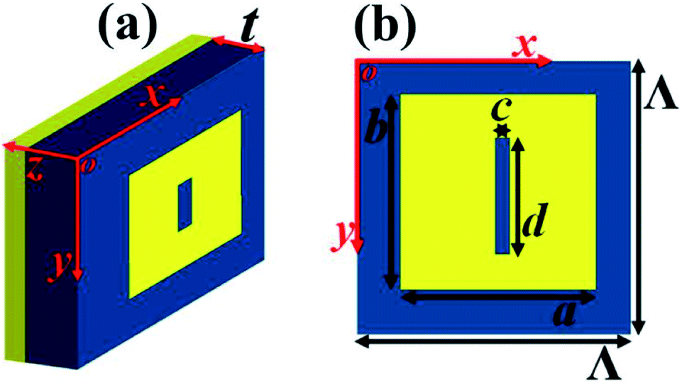 | ||
| Fig. 1 Schematics of the structures of the (a) three-dimensional and (b) two-dimensional triple-band absorption. | ||
To obtain multi-band absorption, the optimized structure parameters are illustrated in Fig. 1(b). The square patch has dimensions of a = b = 80 μm in both the x and y axes. The rectangular hole in the square patch has dimensions of c = 6 μm and d = 42 μm. The unit structure has the repeat period of Λ = 100 μm in the directions of x and y. The gold used here can be considered as a lossy material with a conductivity of 4.09 × 10⁷ S m−1. The commercial software FDTD Solutions, version 8.6, was utilized to analyze the optical properties of the multi-band superabsorber based on the finite-difference time-domain method. In the process of simulation, a plane wave with an electric field along the x-axis was adopted to vertically irradiate the unit structure; periodic boundary conditions along the directions of x and y and perfectly matched layers along the light propagation direction (z-axis) were utilized. The purpose of using periodic boundary conditions was to construct an infinitely arranged structure to match the periodic arrangement, while the purpose of using a perfectly matched layer was to eliminate the influence of unnecessary scattering on the absorption performance.
Results and discussion
The absorption response of the multi-band superabsorber is shown in Fig. 2(a). Three near-perfect absorption resonance bands with narrow bandwidths at frequencies of I = 0.872 THz, II = 2.180 THz, and III = 2.513 THz were realized. Further structure optimization can provide the ability to achieve more absorption bands, such as quad-band absorption (see Fig. 5(f) below). It is well known that for the traditional design methods, a single metallic resonator typically corresponds to a classic absorption peak (or single-band absorption); thus, at least three or four different dimensions of resonators are required to obtain triple-band or quad-band absorption. However, we found here that a square patch with a very small rectangular hole (possibly called the single surface resonance structure) enables triple-band and quad-band absorption; this is interesting and important because the use of this surface structure can play an important role in simplifying the structure design, shortening the structure optimization time and enriching the absorption mechanism. From another view, the design scheme of the given surface structure should have obvious advantages over the traditional design methods using multiple different-sized resonators.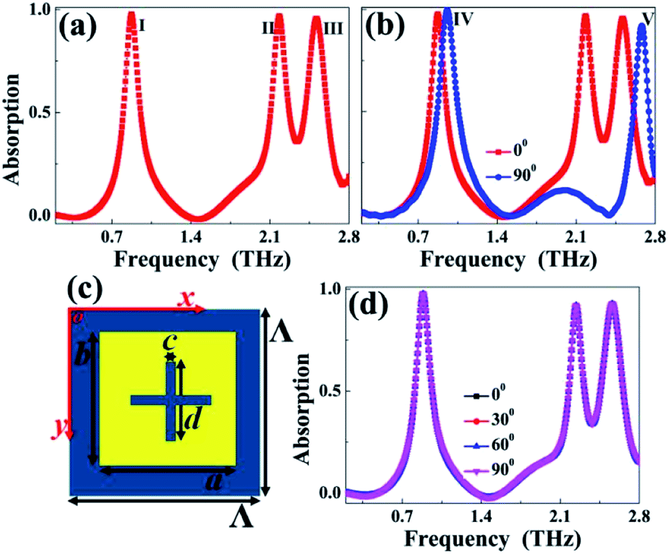 | ||
| Fig. 2 (a) Absorption response of the triple-band superabsorber; (b) absorption response of the triple-band superabsorber under polarization angles of 0° and 90°; (c) structural schematic of the two-dimensional triple-band polarization insensitive superabsorber; (d) absorption response of the triple-band polarization-insensitive superabsorber. | ||
The results further indicate that the performance of the multi-band superabsorber is sensitive to the polarization angle of incident light. As given in Fig. 2(b), when the polarization angle is tuned from the original 0° (electric field along the x-axis) to 90° (electric field along the y-axis), two new resonance bands with very high absorption (>90%) at frequencies of IV = 0.956 THz and V = 2.680 THz can be obtained. We particularly found that the resonance frequency of peak V is about three times that of peak IV, which indicates that modes IV and V should be attributed to the fundamental mode and three-order response of the surface resonator, respectively. Detailed analyses of modes IV and V are provided in the following paragraphs.
As demonstrated in Fig. 2(b), the proposed surface structure shows a polarization-sensitive absorption response. In many cases, however, polarization-insensitive resonance may be a more useful feature. Generally, the simplest and most direct way to obtain polarization-insensitive absorption response is to design a highly symmetrical surface structure. The symmetric structure design can be easily obtained by introducing an additional rectangular hole in the original structure of Fig. 1(b). The size of the newly introduced rectangular hole is the same as that of the original hole, and combining two rectangular holes creates a cross-shaped hole. Fig. 2(c) provides the two-dimensional structure sketch of the triple-band polarization insensitive superabsorber.
As shown, the original rectangular hole is replaced by a cross-shaped hole. It is important to note that other structure parameters, including the sizes of the square patch, the thickness and dielectric constant of the dielectric slab and the repeat period of the unit structure, are unchanged. The simulation results in Fig. 2(d) indeed show polarization-insensitive performance.
Based on the discussion in the above paragraphs, we found that the designed surface structure can achieve not only triple-band polarization sensitivity, but also triple-band polarization insensitivity. Additionally, the surface structure can be further optimized to realize more absorption bands. These resonance features are important because the designed superabsorber can provide considerable freedom to meet the needs of different practical applications.
The resonance mechanism of the triple-band absorption under a 0° polarization angle (i.e., the electric field along the x-axis) is discussed by investigating the near-field distributions of resonance bands I, II, and III, as shown in Fig. 3. As shown in the first row of Fig. 3, the electric field (|E|) distributions of the three absorption peaks are all mainly focused on the edges of the surface structure. This means that the three absorption peaks should result from the localized resonance responses of the surface structure. However, the |E| field aggregation positions of the three absorption peaks in the surface structure are different. The |E| field of peak I in Fig. 3(a) is mostly gathered at the entire edge of the surface resonator along the x-axis, while the |E| field of peak II in Fig. 3(d) (or peak III in Fig. 3(g)) is highly clustered in the four corners of the surface structure (or the middle edge positions of the metallic resonator and both edges of the rectangular hole). That is to say, the localized resonance responses of the surface resonator lead to triple-band absorption. However, unlike the near-field distributions of the traditional unmodified square patch, the introduction of a rectangular hole on the square patch can break the near-field distributions of the traditional unmodified square patch or can rearrange them to form some new and unpredictable resonance modes, thereby generating multi-band absorption.
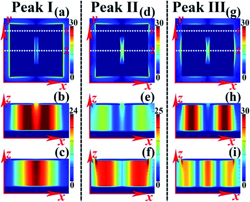 | ||
| Fig. 3 (a), (d), and (g) Electric field (|E|) patterns of absorption peaks I, II, and III of the triple-band absorption, respectively; (b), (e), and (h) magnetic field (|Hy|) patterns of absorption peaks I, II, and III of the triple-band absorption, respectively, in the plane of y = 0, which is parallel to the light propagation direction along the white dotted line 2 of the first; (c), (f), and (i) magnetic field (|Hy|) patterns of absorption peaks I, II, and III of the triple-band absorption, respectively, in the plane of y = 30.5 μm, which is parallel to the light propagation direction along the white dotted line 1 of the first row. | ||
However, the |E| field distributions of these resonance peaks can only qualitatively give the physical origin of the triple-band absorption. To better explore the resonance mechanism of the triple-band absorption, the magnetic field (|Hy|) distributions of the three absorption peaks along the light propagation direction (or the plane that is perpendicular to the unit structure) are provided in the second and third rows of Fig. 3. The |Hy| fields in the second row show the field patterns of the plane y = 0, which is parallel to the light propagation direction along the white dotted line 2 (middle position of the square patch) of the first row of Fig. 3, while the |Hy| field distributions in the plane of y = 30.5 μm, which is parallel to the light propagation direction along the white dotted line 1 (middle position of the upper area of the square patch) of the first row of Fig. 3, are shown in the third row of Fig. 3. As revealed, the |Hy| fields of the three absorption bands are all distributed over the dielectric slab of the multi-band superabsorber, which confirms the localized resonance characteristics of the three absorption bands.
However, the |Hy| field distribution positions of the three absorption bands are different. For resonance peak I, a single strong but similar magnetic field distribution area can be found in the planes of y = 0 (see Fig. 3(b)) and y = 30.5 μm (see Fig. 3(c)), indicating that absorption peak I is the fundamental mode resonance response of the entire metallic resonator.44–46 For resonance peak II, its |Hy| fields are mainly distributed over the plane of y = 30.5 μm (see Fig. 3(f)), while only a small fraction of field distributions can be found in the plane of y = 0 (see Fig. 3(e)). We particularly found that the |Hy| fields in Fig. 3(f) are symmetrically distributed over the dielectric slab of the triple-band superabsorber; this indicates that resonance peak II should result from the coupling of the fundamental mode resonance responses of the left and right sections of the upper area of the surface structure because two-order resonance response cannot be excited under vertical irradiation.47,48
Different from the cases of the resonance peaks I and II, |Hy| fields with two symmetrically distributed aggregation areas (Fig. 3(h)) and three aggregation areas (Fig. 3(i)) were respectively observed. These field distributions show that resonance peak III should be ascribed to the coupling of the fundamental mode resonance responses of the left and right sections of the middle area of the resonator and the three-order response of the upper area of the resonator. In short, by combining three localized resonance responses resulting from the rearrangement of the near-field distribution of the surface resonator, triple-band absorption can be realized. This design scheme using a simple designed surface structure to achieve multi-band absorption should possess many advantages over traditional methods that employ several different dimensions of elements; therefore, the triple-band superabsorber presented here can provide an excellent platform for numerous optoelectronic technology-related applications.
Additionally, according to the field distribution features of resonance peaks IV and V under 90° polarization (when the electric field is polarized along the y-axis), as shown in Fig. 4, resonance absorption peaks IV and V should respectively result from the fundamental mode resonance and three-order response of the surface structure because single strong |Hx| field aggregation area (Fig. 4(b) and (c)) and three strong |Hx| field aggregation areas (Fig. 4(e) and (f)) can be respectively observed for peaks IV and V.44–46
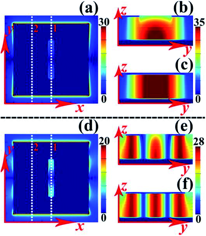 | ||
| Fig. 4 (a) and (d) Electric field (|E|) patterns of absorption peaks IV and V of the suggested resonance structure, respectively, under a polarization angle of 90°; (b) and (c) magnetic field (|Hx|) patterns of absorption peak IV in the planes of x = 0 (parallel to the light propagation direction along the white dotted line 1 in (a)) and x = 21.5 μm (parallel to the light propagation direction along the white dotted line 2 in (a)), respectively; (e) and (f) magnetic field (|Hx|) patterns of absorption peak V in the planes of x = 0 (parallel to the light propagation direction along the white dotted line 1 in (d)) and x = 21.5 μm (parallel to the light propagation direction along the white dotted line 2 in (d)), respectively. | ||
We next evaluate how the changes in the structure parameters affect the absorption performance of the triple-band superabsorber. Here, we mainly discuss the changes in two different parameters: the first parameter is the size of the rectangular hole, and the second parameter is the dimensions of the square patch. As shown in Fig. 5(a), changing the length (c) of the rectangular hole mainly affects the performance of absorption peaks I and III, while the change in absorption peak II can be neglected. Different from the case in Fig. 5(a), the width (d) change of the rectangular hole can strongly affect all absorption peaks; see Fig. 5(b) and (c). We particularly observed that the absorption rate of the resonance peak II has a significant dependence on the width d, as illustrated in Fig. 5(b). The absorption of the resonance peak II can be considered to be suppressed when the width d is equal to 24 μm (or less); see the red and black curves in Fig. 5(b). As a result, the designed multi-band superabsorber can be changed from triple-band absorption to dual-band absorption when a suitable width d is utilized. The simulation results prove that the parameters of the square patch also play important roles in tuning the absorption performance of the triple-band superabsorber. As given in Fig. 5(d) and (e), the frequencies of resonance peaks II and III show large dependence on the patch length a and patch width b, while the changes in the two parameters (a and b) have different effects on the frequency of resonance peak I. The frequency of resonance peak I shows an obvious red-shift when the parameter a is decreased because the |E| fields of peak I are mainly focused on the edges of the resonator along the x-axis, whereas the performance of resonance peak I remains unchanged without reference to parameter b.
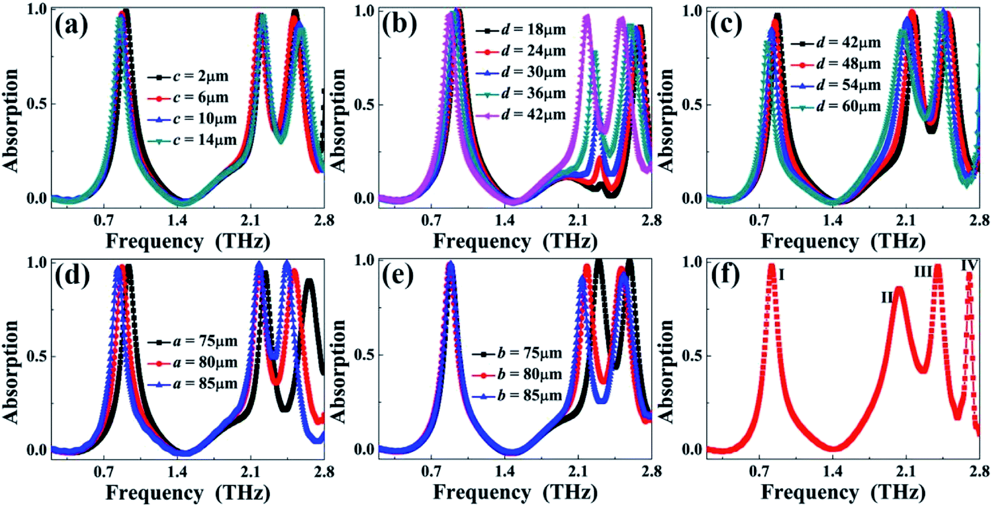 | ||
| Fig. 5 (a) Absorption response of the triple-band superabsorber with changing length (c) of the rectangular hole; (b) and (c) absorption response of the triple-band superabsorber with changing width (d) of the rectangular hole; (c) and (d) absorption responses of the triple-band superabsorber to changes in the length (a) and width (b) of the square patch; (f) absorption response of the designed quad-band superabsorber. | ||
On the basis of the above analysis, we know that the size of the rectangular hole and the dimensions of the square patch are the two key factors to adjust the performance of the triple-band absorption; therefore, the use of appropriate geometrical parameters can meet various application requirements. We further found that the number of the resonance peaks can be increased when the sizes of the resonator are slightly changed. As a typical example, we give the optimization design of quad-band absorption. The three-dimension and two-dimension schematics of the quad-band absorption are respectively shown in Fig. 1(a) and (b), and they are very similar to those of the triple-band absorption. The main differences between the two superabsorbers lie in the parameters of the rectangular hole and the thickness of the dielectric slab. For the quad-band absorption, the length and width of the rectangular hole are respectively c = 4 μm and d = 58 μm, and its dielectric slab thickness is t = 9 μm. Note that the other parameters of quad-band absorption are the same as those of triple-band absorption. Fig. 5(f) shows the absorption response of the given quad-band absorption. As presented, four resonance peaks with large absorptions centered at I = 0.820 THz, II = 2.034 THz, III = 2.404 THz, and IV = 2.701 THz, are realized. Unlike traditional quad-band superabsorbers, in which multiple resonators with different sizes are typically needed,29–38 the quad-band absorption suggested here requires only a single square resonator with a rectangular hole. This is very important in simplifying the structure design, shortening the structure optimization time, removing the strong interaction between the elements, and enriching the mechanism of the multi-band absorption.
The near-field (electric field |E| and magnetic field |Hy|) distributions of absorption peaks I, II, III, and IV are given in Fig. 6 to explore the resonance mechanism of quad-band absorption. Figures (a), (d), (g), and (j) in the first row of Fig. 6 provide the |E| field distributions of peaks I, II, III, and IV, respectively. Figures (b), (e), (h), and (k) of the second row of Fig. 6 respectively show the |Hy| field distributions of peaks I, II, III, and IV along the plane of y = 0 (which is parallel to the light propagation direction along the white dotted line 2 in the first row of Fig. 6). The |Hy| field distributions of peaks I, II, III, and IV along the plane of y = 34.5 μm (which is parallel to the light propagation direction along the white dotted line 1 in the first row of Fig. 6) are respectively provided in (c), (f), (i), and (l) of the third row of Fig. 6. As shown, the |E| fields and |Hy| fields of the four resonant bands are respectively accumulated at the edges of the square patch resonator and the dielectric slab of the quad-band absorption, indicating that the four absorption modes result from the localized resonance responses of the surface resonator.
 | ||
| Fig. 6 (a), (d), (g), and (j) Electric field (|E|) patterns of absorption peaks I, II, III, and IV of the quad-band absorption, respectively; (b), (e), (h), and (k) magnetic field (|Hy|) patterns of absorption peaks I, II, III, and IV of the quad-band absorption, respectively, in the plane of y = 0, which is parallel to the light propagation direction along the white dotted line 2 of the first row; (c), (f), (i), and (l) magnetic field (|Hy|) patterns of absorption peaks I, II, III, and IV of the quad-band absorption, respectively, in the plane of y = 34.5 μm, which is parallel to the light propagation direction along the white dotted line 1 of the first row. | ||
However, the near-field aggregation positions of each resonance absorption mode are different. To be more specific, for resonant peak I, its |E| fields (see Fig. 6(a)) are mainly focused on the entire edges of the left and right sides of the surface structure, and its |Hy| fields in the planes of y = 0 (see Fig. 6(b)) and y = 34.5 μm (see Fig. 6(c)) are very similar in that only a single strong aggregation area can be found. These field distributions provide enough evidence that absorption mode I is the fundamental mode resonance of the entire resonant structure.44–46 For resonance peak II, its |E| fields are mostly concentrated on the four corners of the surface structure and both sides of the rectangular hole, and the |Hy| fields of the absorption mode with symmetric distributions can be observed in the planes of y = 0 (see Fig. 6(e)) and y = 34.5 μm (see Fig. 6(f)). As a result, absorption mode II should be caused by the coupling of the fundamental mode resonance of the left and right sections of the surface structure. According to the near-field aggregation characteristics of absorption mode III (see Fig. 6(g), (h) and (i)), this resonant peak should be derived from the coupling of the fundamental mode resonance of the left and right sections of the middle area of the surface structure and the three-order response of the upper area of the surface structure. Absorption mode IV should result from the three-order resonance of the entire resonant structure because three strong aggregation areas can be simultaneously observed in both planes of y = 0 (see Fig. 6(k)) and y = 34.5 μm (see Fig. 6(l)). Consequently, the superposition of the four discrete resonant bands gives rise to the quad-band absorption.
We further observed that the |E| field patterns of absorption peaks I, II, III, and IV in the rectangular hole are different (see the first row of Fig. 6). Compared to the cases of absorption modes I, III, and IV, the aggregation intensity of the |E| field patterns of resonance mode II is the largest. Generally, large and strong |E| field patterns in a very small space or volume have potential application in sensing-related areas. It can be predicted that the frequency shift range (or the sensing sensitivity) of the second absorption peak II should be larger than that of resonance modes I, III, and IV when some dielectric materials with variable refractive indices are embedded in the rectangular hole.
It can be observed from Fig. 7(b) that the frequency shift of resonant band II is the largest when the refractive index of the embedded dielectric material is varied, which agrees with the theoretical prediction. The frequency shift range of resonance peak II is about 0.511 THz (or 0.170 THz per refractive index unit) when the refractive index of the embedded material is changed from the original air (n = 1) to n = 3. Considering the extremely small volume (4 μm × 58 μm × 0.4 μm) of the embedded material, the sensing sensitivity of the second absorption peak II is quite large, about 1.832 × 10¹⁵ THz per refractive index unit per unit volume. Different from the case of the quad-band absorption, the frequency changes of resonance bands I, II, and III of the triple-band absorption (see Fig. 7(a)) are all nearly unchanged because of the weak or negligible field patterns in the rectangular hole, as shown in the first row in Fig. 3.
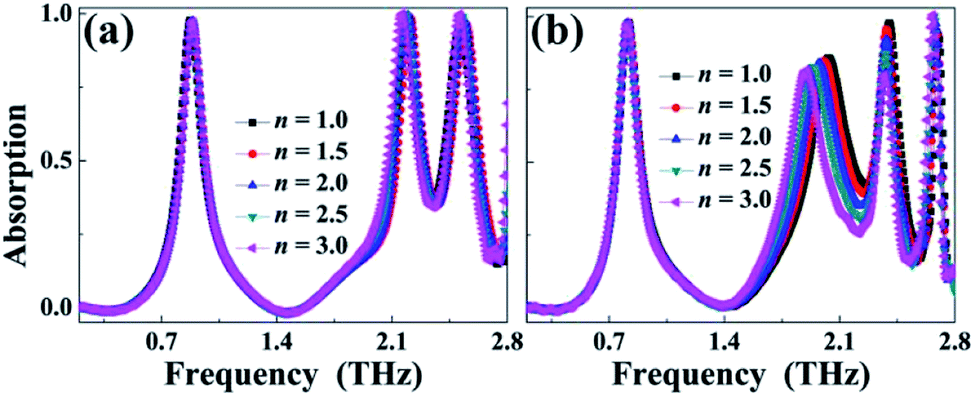 | ||
| Fig. 7 (a) Dependence of the absorption response of the triple-band superabsorber on the refractive index change of the embedded material in the rectangular hole; (b) dependence of the absorption response of the quad-band superabsorber on the refractive index change of the embedded material in the rectangular hole. | ||
Conclusions
In conclusion, a multi-band superabsorber at terahertz frequency is theoretically analyzed. The unit structure of the multi-band absorption is designed by a square metallic patch with a small rectangular hole and a dielectric slab backed by an Au substrate. Three resonance peaks with very high absorbances (>95%) and narrow absorption bandwidths are obtained. Near-field distributions of the three resonant bands are given to provide insight into the physical origin of the triple-band absorption. It is found that the introduction of the rectangular hole in the square patch plays an important role in rearranging the near-field distributions of the unmodified square patch and can generate some new and unpredictable absorption modes and also indirectly reduce the number of resonators, thereby generating triple-band absorption. Based on this, the dimension changes of the rectangular hole and the square patch itself show large influences on the resonance performance of the triple-band absorption.By slightly modifying the parameters of the rectangular hole, the number of resonant peaks of the multi-band superabsorber can be further increased to quad-band absorption, and its operating mechanism is also discussed. Unlike the traditional design strategies of multi-band superabsorbers, which utilize several different-sized resonators, the triple- and quad-band superabsorbers presented here only require a simple design of a surface structure consisting of a single square patch with a rectangular hole, and this design scheme is bound to show numerous advantages compared to previous methods, such as decreasing the number of resonators, shortening the time of structure optimization, and enriching the design ideas of multi-band absorption; therefore, this simplified design of the multi-band superabsorbers can provide a broad platform for many fields of modern optoelectronic technology.
Conflicts of interest
There are no conflicts of interest to declare.Acknowledgements
This research was funded by China Postdoctoral Science Foundation grant number 2019M651692.References
- N. I. Landy, S. Sajuyigbe, J. J. Mock, D. R. Smith and W. J. Padilla, Perfect metamaterial absorber, Phys. Rev. Lett., 2008, 100, 207402 CrossRef CAS PubMed.
- B. A. Munk, Frequency selective surfaces: theory and design, John Wiley & Sons, New York, 2000 Search PubMed.
- W. W. Salisbury, Absorbent body for electromagnetic waves, US Pat., No. 2599944, 1952 Search PubMed.
- C. M. Watts, X. Liu and W. J. Padilla, Metamaterial electromagnetic wave absorbers, Adv. Mater., 2012, 24, OP98 CAS.
- Y. Cui, Y. He, Y. Jin, F. Ding, L. Yang, Y. Ye, S. Zhong, Y. Lin and S. He, Plasmonic and metamaterial structures as electromagnetic absorbers, Laser Photonics Rev., 2014, 8, 495 CrossRef CAS.
- X. Liu, K. Bi, B. Li, Q. Zhao and J. Zhou, Metamaterial perfect absorber based on artificial dielectric atoms, Opt. Express, 2016, 24, 20454 CrossRef CAS PubMed.
- M. Lei, N. Feng, Q. Wang, Y. Hao, S. Huang and K. Bi, Magnetically tunable metamaterial perfect absorber, J. Appl. Phys., 2016, 119, 244504 CrossRef.
- B. X. Wang, X. Zhai, G. Z. Wang, W. Q. Huang and L. L. Wang, A novel dual-band terahertz metamaterial absorber for a sensor application, J. Appl. Phys., 2015, 117 Search PubMed.
- B. X. Wang, Y. He, P. Lou and W. Xing, Design of a dual-band terahertz metamaterial absorber using two identical square patches for sensing application, Nanoscale Adv., 2020, 2, 763 RSC.
- W. C. Chen, A. Cardin, M. Koirala, X. Liu, T. Tyler, K. G. West, C. M. Bingham, T. Starr, A. F. Starr, N. M. Jokerst and W. J. Padilla, Role of surface electromagnetic waves in metamaterial absorbers, Opt. Express, 2016, 24, 6783 CrossRef CAS PubMed.
- M. D. Astorino, F. Frezza and N. Tedeschi, Ultra-thin narrow-band, complementary narrow-band, and dual-band metamaterial absorbers for applications in the THz regime, J. Appl. Phys., 2017, 121, 063103 CrossRef.
- O. Ayop, M. K. A. Rahim, N. A. Murad, N. A. Samsuri, F. Zubir and H. A. Majid, Dual-band metamaterial perfect absorber with nearly polarization-independent, Appl. Phys. A, 2017, 123, 63 CrossRef.
- X. Liu, C. Lan, B. Li, Q. Zhao and J. Zhou, Dual band metamaterial perfect absorber based on artificial dielectric molecules, Sci. Rep., 2016, 6, 28906 CrossRef CAS PubMed.
- Y. Zhang, T. Li, Q. Chen, H. Zhang, J. F. Ohara, E. Abele, A. J. Taylor, H. T. Chen and A. K. Azad, Independently tunable dual-band perfect absorber based on graphene at mid-infrared frequencies, Sci. Rep., 2015, 5, 18463 CrossRef CAS PubMed.
- B. X. Wang, G. Z. Wang and L. L. Wang, Design of a novel dual-band terahertz metamaterial absorber, Plasmonics, 2016, 11, 523 CrossRef CAS.
- B. X. Wang, G. Z. Wang and T. Sang, Simple design of novel triple-band terahertz metamaterial absorber for sensing application, J. Phys. D: Appl. Phys., 2016, 49, 165307 CrossRef.
- J. W. Park, P. V. Tuong, J. Y. Rhee, K. W. Kim, W. H. Jang, E. H. Choi, L. Y. Chen and Y. P. Lee, Multi-band metamaterial absorber based on the arrangement of donut-type resonators, Opt. Express, 2013, 21, 9691 CrossRef PubMed.
- R. Wang, L. Li, J. Liu, F. Yan, F. Tian, H. Tian, J. Zhang and W. Sun, Triple-band tunable perfect terahertz metamaterial absorber with liquid crystal, Opt. Express, 2017, 25, 32280 CrossRef CAS.
- N. Mishra, D. K. Choudhary, R. Chowdhury, K. Kumari and R. K. Chaudhary, An investigation on compact ultra-thin triple band polarization independent metamaterial absorber for microwave frequency applications, IEEE Access, 2017, 5, 4370 Search PubMed.
- M. Obaidullah, V. Esat and C. Sabah, Polarization independent triple-band (5,4) semiconducting carbon nanotube metamaterial absorber design for visible and ultraviolet regions, J. Nanophotonics, 2017, 11, 046011 Search PubMed.
- G. Kajtar, M. Kafesaki, E. N. Economou and C. M. Soukoulis, Theoretical model of homogeneous metal-insulator-metal perfect multi-band absorbers for the visible spectrum, J. Phys. D: Appl. Phys., 2016, 49, 055104 CrossRef.
- S. Bhattacharyya and K. V. Srivastava, Triple band polarization-independent ultra-thin metamaterial absorber using electric field-driven LC resonator, J. Appl. Phys., 2014, 115, 064508 CrossRef.
- T. M. Kollatou, A. I. Dimitriadis, S. D. Assimonis, N. V. Kantartzis and C. S. Antonopoulos, Multi-band, highly absorbing, microwave metamaterial structures, Appl. Phys. A, 2014, 115, 555 CrossRef CAS.
- J. Chen, Z. Hu, S. Wang, X. Huang and M. Liu, A triple-band, polarization- and incident-independent microwave metamaterial absorber with interference theory, Eur. Phys. J. B, 2016, 89, 14 CrossRef.
- H. Zhai, C. Zhan, Z. Li and C. Liang, A triple-band ultrathin metamaterial absorber with wide-angle and polarization stability, IEEE Antennas Wirel. Propag. Lett., 2015, 14, 241 Search PubMed.
- B. Zhang, J. Hendrickson and J. Guo, Multispectral near-perfect metamaterial absorbers using spatially multiplexed plasmon resonance metal square structures, J. Opt. Soc. Am. B, 2013, 30, 656 CrossRef CAS.
- X. Shen, Y. Yang, Y. Zang, J. Gu, J. Han, W. Zhang and T. J. Cui, Triple-band terahertz metamaterial absorber: Design, experiment, and physical interpretation, Appl. Phys. Lett., 2012, 101, 154102 CrossRef.
- B. X. Wang, C. Tang, Q. Niu, Y. He and T. Chen, Design of narrow discrete distances of dual-/triple-band terahertz metamaterial absorbers, Nanoscale Res. Lett., 2019, 14, 64 CrossRef PubMed.
- S. Liu, J. Zhuge, S. Ma, H. Chen, D. Bao, Q. He, L. Zhou and T. J. Cui, A bi-layered quad-band metamaterial absorber at terahertz frequencies, J. Appl. Phys., 2015, 118, 245304 CrossRef.
- D. Xiao and K. Tao, Ultra-compact metamaterial absorber for multiband light absorption at mid-infrared frequencies, Appl. Phys. Express, 2015, 8, 102001 CrossRef.
- M. Agarwal, A. K. Behera and M. K. Meshram, Wide-angle quad-band polarisation-insensitive metamaterial absorber, Electron. Lett., 2016, 52, 340 CrossRef CAS.
- D. Chaurasiya, S. Ghosh, S. Bhattacharyya and K. V. Srivastava, An ultrathin quad-band polarization-insensitive wide-angle metamaterial absorber, Microw. Opt. Technol. Lett., 2015, 57, 697 CrossRef.
- A. Sarkhel and S. R. B. Chaudhuri, Compact quad-band polarization-insensitive ultrathin metamaterial absorber with wide angle stability, IEEE Antennas Wirel. Propag. Lett., 2017, 16, 3240 Search PubMed.
- B. X. Wang, X. Zhai, G. Z. Wang, W. Q. Huang and L. L. Wang, Design of a four-band and polarization-insensitive terahertz metamaterial absorber, IEEE Photonics J., 2015, 7, 4600108 Search PubMed.
- W. Wang, M. Yan, Y. Pang, J. Wang, H. Ma, S. Qu, H. Chen, C. Xu and M. Feng, Ultra-thin quadri-band metamaterial absorber based on spiral structure, Appl. Phys. A, 2015, 118, 443 CrossRef CAS.
- Y. H. Ren, J. Ding, C. J. Guo, Y. Qu and Y. C. Song, Design of a quad-band wide-angle microwave metamaterial absorber, J. Electron. Mater., 2017, 46, 370 CrossRef CAS.
- B. X. Wang, Y. He, P. Lou, W. Q. Huang and F. Pi, Penta-band terahertz light absorber using five localized resonance responses of three patterned resonators, Results Phys., 2020, 16, 102930 CrossRef.
- B. X. Wang, Quad-band terahertz metamaterial absorber based on the combining of the dipole and quadrupole resonances of two SRRs, IEEE J. Sel. Top. Quantum Electron., 2017, 23, 4700107 Search PubMed.
- Y. J. Kim, Y. J. Yoo, K. W. Kim, J. Y. Rhee, Y. H. Kim and Y. P. Lee, Dual broadband metamaterial absorber, Opt. Express, 2015, 23, 3861 CrossRef CAS PubMed.
- J. Zhu, Z. Ma, W. Sun, F. Ding, Q. He, L. Zhou and Y. Ma, Ultra-broadband terahertz metamaterial absorber, Appl. Phys. Lett., 2014, 105, 021102 CrossRef.
- P. Liu and T. Lan, Wide-angle, polarization-insensitive, and broadband metamaterial absorber based on multilayered metal-dielectric structures, Appl. Opt., 2017, 56, 4201 CrossRef CAS PubMed.
- C. Zhang, Q. Cheng, J. Yang, J. Zhao and T. J. Tie, Broadband metamaterial for optical transparency and microwave absorption, Appl. Phys. Lett., 2017, 110, 143511 CrossRef.
- M. Luo, S. Shen, L. Zhou, S. Wu, Y. Zhou and L. Chen, Broadband, wide-angle, and polarization-independent metamaterial absorber for the visible regime, Opt. Express, 2017, 25, 16715 CrossRef CAS PubMed.
- G. Dayal and S. A. Ramakrishna, Multipolar localized resonances for multi-band metamaterial perfect absorbers, J. Opt., 2014, 16, 094016 CrossRef CAS.
- B. X. Wang, Single-patterned metamaterial structure enabling multi-band perfect absorption, Plasmonics, 2017, 12, 95 CrossRef CAS.
- A. Sellier, T. V. Teperik and A. Lustrace, Resonant circuit model for efficient metamaterial absorber, Opt. Express, 2013, 21, A997 CrossRef PubMed.
- J. Hao, L. Zhou and M. Qiu, Nearly total absorption of light and heat generation by plasmonic metamaterials, Phys. Rev. B, 2011, 83, 165107 CrossRef.
- J. Wang, Y. Chen, J. Hao, M. Yan and M. Qiu, Shape-dependent absorption characteristics of three-layered metamaterial absorbers at near-infrared, J. Appl. Phys., 2011, 109, 074510 CrossRef.
- Z. Li, S. Butun and K. Aydin, Large-area, lithography-free super absorbers and color filters at visible frequencies using ultrathin metallic films, ACS Photonics, 2015, 2, 183 CrossRef CAS.
- V. Caligiuri, M. Palei, G. Biffi, S. Artyukhin and R. Krahne, A semi-classical view on epsilon-near-zero resonant tunneling modes in metal/insulator/metal nanocavities, Nano Lett., 2019, 19, 3151 CrossRef CAS PubMed.
- Z. Sakotic, A. Krasnok, N. Cselyuszka, N. Jankovic and A. Alu, Berreman embedded eigenstates for narrow-band absorption and thermal emission, Phys. Rev. Appl., 2020, 13, 064073 CrossRef CAS.
- K. Halterman and M. Alidoust, Waveguide modes in Weyl semimetals with tilted dirac cones, Opt. Express, 2019, 27, 36164 CrossRef CAS PubMed.
- L. Huang, D. R. Chowdhury, S. Ramani, M. T. Reiten, S. N. Luo, A. K. Azad, A. J. Taylor and H. T. Chen, Impact of resonator geometry and its coupling with ground plane on ultrathin metamaterial perfect absorbers, Appl. Phys. Lett., 2012, 101, 101102 CrossRef.
| This journal is © The Royal Society of Chemistry 2021 |