
 Open Access Article
 This Open Access Article is licensed under a Creative Commons Attribution-Non Commercial 3.0 Unported Licence
Shaping graphene with optical forging: from a single blister to complex 3D structures†
Kamila K.
Mentel
 a,
Jyrki
Manninen
b,
Vesa-Matti
Hiltunen
b,
Pasi
Myllyperkiö
a,
Andreas
Johansson
ab and
Mika
Pettersson
*a
a,
Jyrki
Manninen
b,
Vesa-Matti
Hiltunen
b,
Pasi
Myllyperkiö
a,
Andreas
Johansson
ab and
Mika
Pettersson
*a
aNanoscience Center, Department of Chemistry, University of Jyväskylä, Finland. E-mail: mika.j.pettersson@jyu.fi
bNanoscience Center, Department of Physics, University of Jyväskylä, Finland
First published on 5th January 2021
Abstract
Properties of graphene, such as electrical conduction and rigidity can be tuned by introducing local strain or defects into its lattice. We used optical forging, a direct laser writing method, under an inert gas atmosphere, to produce complex 3D patterns of single layer graphene. We observed bulging of graphene out of the plane due to defect induced lattice expansion. By applying low peak fluences, we obtained a 3D-shaped graphene surface without either ablating it or deforming the underlying Si/SiO2 substrate. We used micromachining theory to estimate the single-pulse modification threshold fluence of graphene, which was 8.3 mJ cm−2, being an order of magnitude lower than the threshold for ablation. The control of exposure parameters allowed the preparation of blisters with various topographies. The optically forged structures were studied with atomic force microscopy and Raman spectroscopy. Optically forged blisters act as building blocks in the formation of more complex structures. We found a simple geometric rule that helps to predict the shape of complex patterns which are created by the overlapping multiple exposures. Optical forging enables writing of extended patterns with diffraction unlimited features, which makes this method promising in the production of nanodevices with locally induced surface modifications.
Introduction
Femtosecond laser micromachining is a well-established method in the fabrication of micrometer-scale patterns and three-dimensional devices, thanks to the beneficial properties of the method, such as sub-micrometer scale precision, mask-free processing and confinement of the induced changes to the laser focal volume.1,2 Recently, laser micromachining has gained more attention in the alteration of the physical or chemical properties of 2D materials. It was shown to be useful in localized modification and thinning of multilayered graphene,3 and 2D MoS2,4 WS2,5 and PdSe2.6 Direct laser patterning was used for phase transformation of 2D PdSe2.6 It was used in micro-cutting,7,8 in ablation of graphene,9–13 and in producing micro and nano-disks.14 Direct laser writing was also applied for graphene oxide reduction,15 for oxidation of graphene in a controlled manner,16,17 and patterning of the p–n junction in graphene.18Recently, we demonstrated that optical forging, a direct laser writing method with a tightly focused femtosecond laser beam under an inert gas atmosphere, can be used for 3D shaping of graphene.19–21 Optical forging leads to controllably induced defects, causing lattice expansion and bulging of graphene out of the plane. With a sufficiently large optical forging dose, graphene exhibits strong luminescence.21
In this study, we present how optical forging can be used to create spatially precise and well-defined 3D patterns in a single layer of graphene. By careful choice of femtosecond laser exposure parameters, we induce a desired amount of defects over a spatially confined region on the chip surface. Depending on the laser parameters, the shape of the primary laser writing element varies from a Gaussian-shaped dome to a ring structure with sub-diffraction limited ripples.20 Overlapping basic writing elements leads to extended patterns, the shapes of which depend on the sequence of writing of discrete elements. The overall appearance of the patterns follows a simple geometric rule. These systematic studies on step-by-step optical forging provide basic know-how for complex design and 3D shaping of graphene. The presented method enables writing of extended patterns of 3D objects having feature sizes down to, and even below, 100 nm at the FWHM, while using a far-field laser beam. The introduced out-of-plane deformation in graphene additionally forms a basis for strain engineering of its electronic and photonic properties.22 This method possibly can be expanded to other 2D materials, opening an exciting new perspective of modification of atomically thin materials.
Experimental section
Sample fabrication
For both samples used in this study, the graphene was synthesized on Cu(111) thin films evaporated onto single crystal sapphire (0001) substrates. The catalyst film was annealed at 1070 °C under gas flows of 470 sccm argon and 30 sccm hydrogen for 45 minutes. After annealing, the graphene growth was initiated by injecting 2 sccm of 1% methane in argon to the furnace while keeping the temperature at 1070 °C. The growth time was 7 minutes. After the growth, the samples were taken out of the hot zone of the furnace and allowed to cool down.The graphene films were transferred by a standard PMMA transfer method23 onto a target substrate, which was a silicon chip with a 300 nm thermal oxide film and a metal marker grid on top. The samples were spin-coated with a PMMA layer and the copper was etched in 1 M ammonium persulfate solution leaving the graphene/PMMA stack floating on the liquid. Then the graphene was rinsed in DI water, placed in 12% HCl to remove possible metal residues, rinsed again in DI water and placed onto the Si/SiO2 substrate. The samples were baked on a hot plate at 120 °C for 5 minutes to evaporate water between the substrate and the graphene. After this the PMMA film was removed with acetone and IPA. Sample 1 was annealed first at 200 °C in an O2 atmosphere for 30 minutes, then at 300 °C in an Ar/H2 atmosphere for two hours and finally at 300 °C in an O2 atmosphere for two hours. Sample 2 was annealed at 300 °C in an Ar/H2 atmosphere for two hours to remove PMMA residues.
Optical forging
Direct laser writing of the patterns was performed with a 515 nm femtosecond laser (Pharos-10, Light Conversion Ltd., 600 kHz, 250 fs pulse duration) focused with an objective lens (N.A. = 0.8) to a Gaussian spot. Detailed setup description was presented previously.19 The laser writing was performed under a nitrogen purge to prevent photo-oxidation of graphene during the writing process. The pulse energies were varied between 20 and 120 pJ. Blisters were irradiated by single spot exposure with irradiation time from 0.1 to 300 s per spot. The complex patterns were prepared by step-by-step irradiation with separation distances between consecutive laser spots of up to 1.5 μm.All presented data belong to the optical forging studies performed on sample 1. An exception is etching data which were obtained from sample 2.
AFM characterization
AFM imaging was made on a Bruker Dimension Icon Atomic Force Microscope (AFM) in the PeakForce Quantitative Nanomechanical Mapping (QNM) mode. ScanAsyst Air probes from Bruker were used during imaging with the peak force limited to 2 nN. The diameter of the blisters was estimated from the collected height image. The Bearing Analysis tool from Nanoscope Analysis 1.9 software was used to estimate the volume expansion of created structures. This tool allows to obtain information about how much surface lies above or below a given height. In the analysis, the AFM height image of each forged blister is sliced at a specified height, ΔZ. A plane drawn at the ΔZ gives an area that is occupied by a region above the indicated background level. By summing areas for each ΔZ between 0 < ΔZ ≤ Zmax, where Zmax is the height of the blister, the bearing volume information of the 3D structures is obtained.Raman characterization
Raman measurements were carried out with a home-built Raman setup in a backscattering geometry using a 532 nm excitation wavelength produced with a continuous wave single frequency laser (Alphalas, Monolas-532-100-SM). Detailed setup description was presented previously.17 Mapping was conducted using 250 nm steps between measurement points. A laser power of ∼0.25 mW was utilized. Two accumulations per each point were collected with 6 s measurement time per accumulation.Oxygen plasma etching
Oxygen plasma etching was carried out using an Oxford Instruments Plasmalab 80 Plus reactive ion etcher. Plasma was generated using a 30 mT magnetic field at a chamber pressure of 30 mTorr and an oxygen flow of 30 sccm. The etching was performed with a forward power setting of 20 W for 30 s on sample 2.Results and discussion
Optical forging experiments were performed in an inert atmosphere to prevent oxidative processes.19 We used tightly focused pulses with a 515 nm wavelength and 250 fs duration at a 600 kHz repetition rate to modify the graphene surface. In order to determine the influence of the laser dose on the shape of the forged blisters we prepared a series of laser exposures with increasing pulse energies (20–120 pJ) and irradiation times per spot (0.1–300 s), which corresponds to 6 × 10⁴ to 1.8 × 10⁸ applied laser pulses per spot. The laser dose is described as the pulse energy multiplied with irradiation time per spot and divided by the laser spot size, expressed in pJ s cm−2. The blister topography profile was subsequently characterized by atomic force microscopy (Fig. 1a). A single blister is the smallest unit which can be forged. Thanks to the reproducibility of the process, for which an example is presented in Fig. S1,† the blister can be used as a building block to create large and complex structures (presented later). By changing exposure parameters, we gained control over produced blister features such as its height, outer diameter, and complexity (e.g. more than one fringe). The cross-sections of blisters are presented in Fig. S2.† Blisters are relatively plastic, and their shape changes upon further irradiation.20 An increase in dose increases the overall diameter, D, of the formed pattern, which follows logarithmic dependence (Fig. 1b). Blisters with diameters below 1.1 μm exhibit a dome-like structure. Increasing the laser dose introduces a pit in the blister (D = 1.15–1.25 μm), until at higher doses, a single ring-like fringe is formed (1.25 < D < 1.3 μm). Further irradiation causes the appearance of a central dome and/or more fringes (D > 1.3 μm). The blisters have features that are significantly below the diffraction limit as was observed previously.20 For example, the ring can have a linewidth of 100 nm. It was suggested that the diffraction-unlimited rippling occurs due to the interplay between surface adhesion and stress induced lattice expansion.20 Additionally, blisters with diameters equal to or larger than the beam size exhibit an increase in the surface roughness.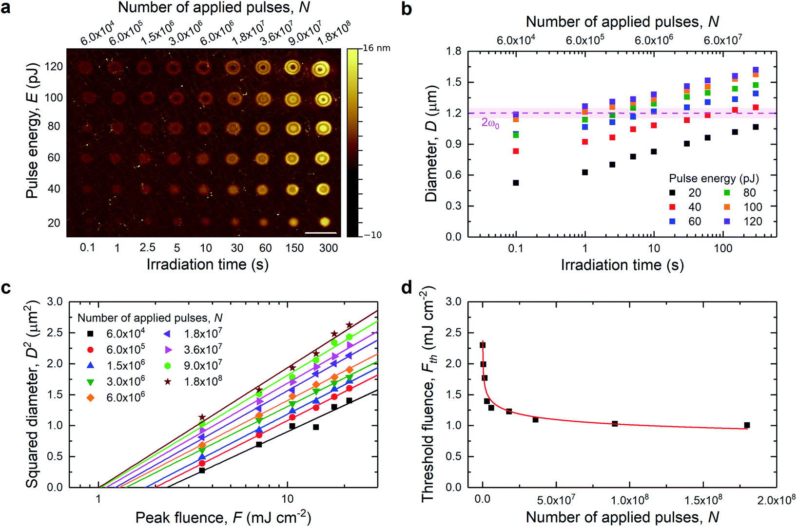 | ||
| Fig. 1 (a) AFM topography image of blisters formed at different exposure times and laser pulse energies. Scale bar 2.5 μm. (b) Blister diameter as a function of irradiation time (number of applied pulses). Dashed line shows an estimated beam diameter with its uncertainty (pink shade). (c) Squared blister diameter as a function of peak fluence. (d) Calculated laser threshold fluences for N-pulses plotted versus the number of applied pulses with presented fitting of the power law from eqn (3) (red line). | ||
We used well-established equations for the ablation threshold in laser micromachining in order to obtain a modification threshold fluence, Fth(N), for optical forging.24 For applied N-pulses, the Fth(N) can be determined from a plot of the squared diameter of the forged blister, D2, versus the laser peak fluence, F, deposited on the sample related by:24
 | (1) |
 | (2) |
Eqn (2) shows a linear dependence between the laser pulse energy and the peak fluence. Thus, the beam radius can be obtained from plotting D2versus ln(E). The average beam radius was estimated to be ω0 = 0.60 ± 0.02 μm at 1/e2 and was used to calculate the laser peak fluence from eqn (2). The squared diameter as a function of applied laser peak fluence is presented in Fig. 1c. The modification threshold fluence for N-pulses was obtained by extrapolation of D2 to zero. The estimated threshold fluence was 2.3 mJ cm−2 for an irradiation time of 0.1 s (6 × 10⁴ pulses), and it decreased with the number of applied laser pulses. The obtained Fth(N) values as a function of applied laser pulses are plotted in Fig. 1d. The behavior of lowering threshold fluences can be associated with an incubation effect.25 This effect can be related e.g. to plastic deformation,26 heat accumulation,27 and defect formation.28 It was reported that in a graphene/SiO2/Si stack, most of the significant absorption occurs in the graphene layer.29 In addition, due to the use of relatively short laser pulses (250 fs) and very low fluences (F < 25 mJ cm−2), we can possibly exclude heat accumulation in our sample. In our system, the incubation effect can be assigned to defect formation due to laser exposure. This is supported by Fig. S3 and S4,† where we show Raman spectra collected for optically forged blisters presented in Fig. 1a. Blisters prepared with short exposures exhibit narrow D bands, which correspond to introduction of point defects into the graphene lattice. An estimated point defect density in non-irradiated graphene is approximately 1011 cm−2, and it rapidly increases for the blisters prepared using low laser doses (<2 × 10¹² pJ s cm−2) up to 5 × 1011 cm−2. Higher doses increase point defect density at a slower rate up to 1012 cm−2. Longer laser exposures and/or increased pulse energies trigger a broadening of D and G bands and increase the intensity of a broad background. Both changes support an increasing disorder in the graphene lattice. The observed behavior was associated in our previous study with the formation of line defects.21 Nonetheless, all blisters continue to exhibit spectral features of graphene, confirming that the applied low range of fluences does not lead to ablation. We proposed the Stone–Wales defects19,21 as plausible point defects created in the graphene lattice, which can gradually develop into extended line defects.21 We note that in studies by other groups of laser-induced ablation of graphene,30,31 a blistering effect was not observed. We also stress that the blisters in the present study are smooth and have well-defined shapes, with no signs of missing layer fragments. Moreover, we have shown that pronounced bulging of graphene out of the plane occurs only for optical forging experiments performed under an inert atmosphere, where oxidative processes are excluded.19 To our knowledge this is the first time when micromachining equations were successfully applied to laser-induced graphene modification studies, when the material is still intact, not partially or fully ablated. This is due to visible blistering which allows us to accurately estimate the diameter of the laser affected area.
To find the relation between single pulse exposure and N-pulse threshold fluence we used the equation:25
| Fth(N) = Fth(1)NS−1 | (3) |
For completeness, we will also consider the effect of the laser exposure on the underlying substrate of 300 nm SiO2 on Si. Rublack et al. reported single-pulse ablation and the melting threshold for 100 nm SiO2 on the Si substrate to be 219 ± 4 mJ cm−2 and 137 ± 2 mJ cm−2, respectively (λex = 515 nm, 280 fs).33 Above the melting threshold, a delamination of the SiO2 layer may occur. In our experiments we used similar laser parameters (excitation wavelength, pulse duration), and therefore, we can make direct comparison. Our estimated Fth(1) value for graphene modification is 25-times lower than the ablation threshold and 16.5 times lower than the melting threshold for single-pulse fluences of a SiO2 layer. It is worth mentioning that the nature of the delamination and consequent visible bulging of a thin SiO2 layer is different than in graphene. The bulging of a SiO2 layer or other thin layer materials is a pressure induced lift off by melting and vaporizing of the silicon layer underneath.34–36 In graphene, bulging presumably occurs by the expansion of the material lattice due to the presence of laser-induced defects. The obtained modification threshold value is also ∼25 times lower than the reported single-shot ablation threshold fluence for silicon, Fth(1) = 220 mJ cm−2 (λex = 515 nm, 3 ps).37 The fluences used in this study (F < 25 mJ cm−2) are therefore too low to introduce any changes to the substrate. This was confirmed by removing optically forged graphene squares through O2 plasma etching. Subsequent AFM imaging revealed an intact surface underneath the removed graphene squares (Fig. S5†).
In laser micromachining, the volume of created holes/craters is frequently studied in order to provide information about the quality of the ablation process. In our studies we do not create holes in the material, but we fabricate blisters which are bulging out of the plane. These structures can also be described with a volume parameter. We estimated the volume of expanded blisters using the bearing analysis tool in Nanoscope Analysis 1.9 software (Fig. 2a). Blisters created with 40 to 120 pJ pulse energies follow the same trend. Blisters formed upon irradiation with 20 pJ seem to have bit smaller volumes, but they also exhibit smaller diameters. From Fig. 2b it is visible that the squared volume expansion, V2 increases linearly as a function of the applied laser dose. Fig. 2c shows three pairs of blisters formed with the same dose: 0.11 × 10¹², 1.06 × 10¹² and 1.59 × 10¹² pJ s cm−2. Each pair exhibits similar volume expansion, however, possesses disparate shape/cross sections. This could possibly be explained by different initial irradiation conditions. Higher laser pulse energy produces blisters with a larger lateral diameter and more pronounced ring structures, whereas lower laser pulse energy and longer exposure produce blisters with a smaller footprint and more dome shaped structures.
 | ||
| Fig. 2 (a) Estimated volume of blisters and (b) squared volume as a function of applied laser dose. Dashed line represents least square fitting to the points between 40 and 120 pJ. (c) AFM images of pairs of blisters prepared with the same dose: 0.11 × 10¹², 1.06 × 10¹² and 1.59 × 10¹² pJ s cm−2 and their corresponding vertical cross-section (marked by arrows). Above each AFM image, irradiation conditions are presented: pulse energy and irradiation time. Scale bar 0.5 μm. | ||
We used our AFM's PeakForce Quantitative Nanomechanical Mapping (QNM) mode to characterize the mechanical properties of graphene before and after optical forging. We collected data on qualitative changes in adhesion, elastic modulus (fitted with Derjaguin–Muller–Toporov model, DMT-modulus)38 and deformation together with the topography measurements. The collected data are presented in Fig. S6.† All types of data show a clear difference between irradiated and non-irradiated areas. The adhesion data provide information about the adhesion between the studied surface and the silicon tip. We noticed that the adhesion is reduced in the area of irradiated spots in comparison to pristine graphene, with the lowest value found on the blister fringes, and on the central domes for blisters larger than the beam size. Essentially, the lowest adhesion corresponds to the highest part of the blisters. This may indicate that graphene is detached from the substrate, and therefore, a smaller area of the sample interacts with the tip leading to the smaller adhesion forces. The reduction of the adhesive forces was associated with the delamination of graphene crumples from the substrate in other studies.39 The deformation data give information about deformability of the sample upon pressing with the AFM tip. The highest recorded deformation does not correspond to the most elevated region of the blister. It is located on the shoulder of dome-like blisters and outer side of the fringe of ring-like blisters, meaning that this is the softest part. Assuming that blisters are empty inside, they can flex sideways under the load on the outer side of the fringe. This bending would show as increased deformation. Additionally, the outer side of the blister should contain fewer defects, which can be correlated with the shape of the gaussian beam, leading to lower irradiation intensity at the edges. Larger lattice disorder should occur closer to the center of the beam. The relative values of the DMT modulus show that the rigidity of the nanomaterial increases under laser exposure with respect to the pristine graphene. However, used forces are too small to induce material deformation in the in-plane direction, and therefore, it is not certain if we observed just structural flexing, or also real material properties. Blisters with the broad Raman background have higher elastic modulus values. Structures with additional central domes/or extra fringes exhibit mixed stiffness properties, due to high surface roughness. Change in the mechanical properties of graphene is associated with the presence of defects. The rigidity of graphene will depend on the amount and type of introduced defects. It was reported that divacancy always reduces the stiffness of graphene, while it is unclear if a moderate number of sp3-type defects increase the sample stiffness40,41 However, experimental studies on the relation between graphene stiffness and defect concentration are still limited. The correlation of high stiffness with the existence of line defects in our studies needs to be verified by further experiments.
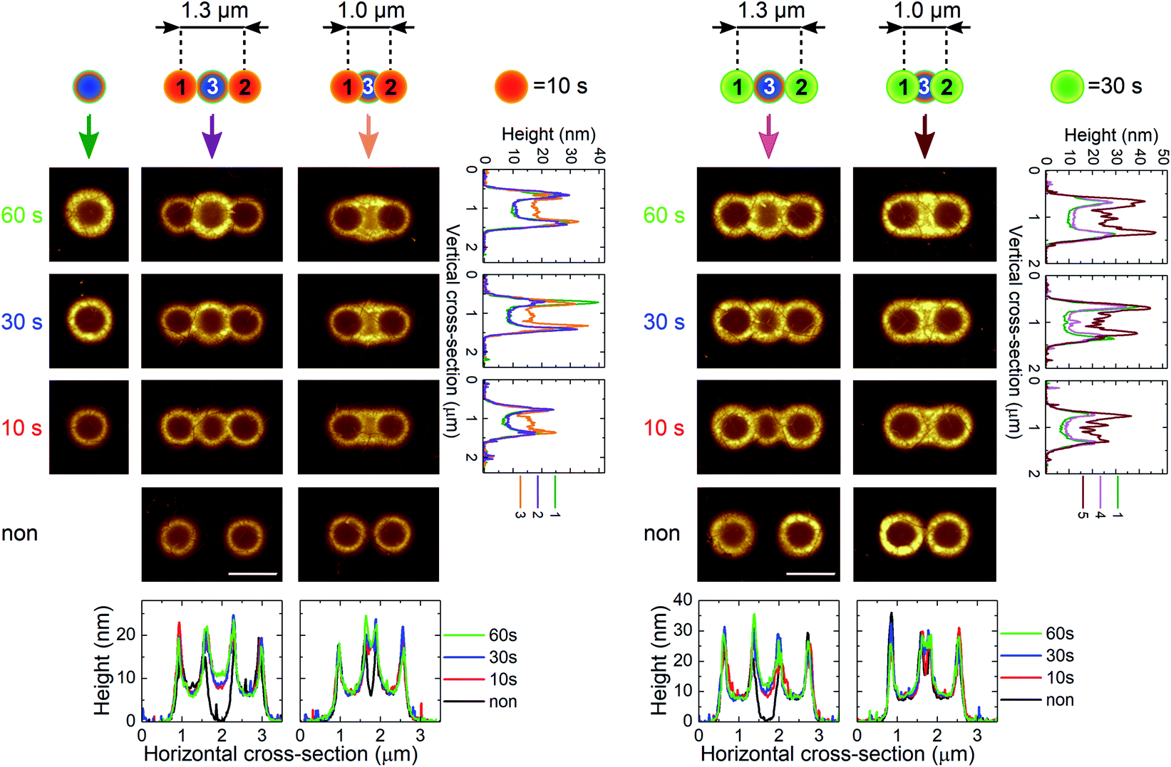
After establishing the connection between the irradiation dose and blister shape, we tested forming patterns through multistep irradiation of basic writing elements. The simplest example is a dimer of blisters. In Fig. 3a we show the schematic illustration of dimer formation by two-step irradiation with varying horizontal distance, Δx, between the laser spots. When Δx = 1.3 μm the blisters do not intersect, while for Δx = 0 μm they fully overlap. In each pair, the blister on the left was created (optically forged) first. Fig. 3a also contains AFM images of 6 sets of optically forged dimers prepared by varying irradiation times: 10 s/60 s, 10 s/30 s, 10 s/10 s, 30 s/30 s and 60 s/60 s. One of the most striking observations is that the structure of the first blister is always maintained. The second laser exposure cannot deform the overall shape of the previously formed blister but forms a 3D shape under the part of the beam exposing an area of pristine graphene. However, it can subtly expand the first blister by following the volume to dose dependence. This can be seen in the cross-section of the dimers presented in Fig. 3b and c. The profile of the first blister stays virtually the same after the second laser exposure. Small changes can be seen for full overlap and longer exposure such as the 60 s/60 s dimer pair. A full overlap mainly causes lattice expansion on the fringe exterior. In the case of the 60 s/60 s dimer pair, a slight hint of the presence of a central dome starts to be visible. This agrees with the blister growth rule, which stipulates that a dome-like blister evolves into a fringe-like blister and then into a fringe-like blister with a central dome structure with increasing irradiation dose.
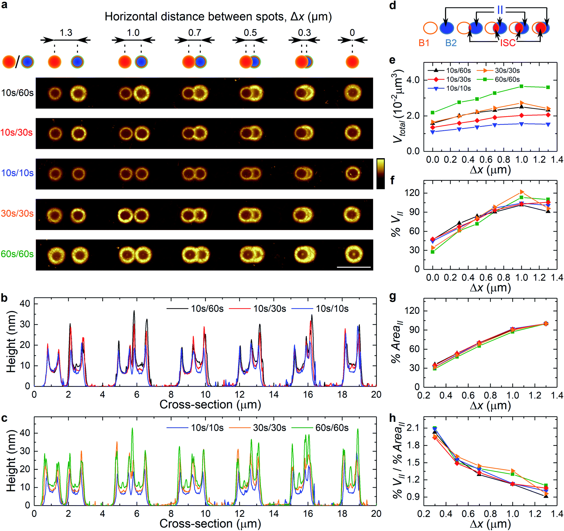 | ||
| Fig. 3 (a) Illustration of dimer overlap with various separation distances, Δx, and the AFM images of optically forged dimers created with 60 pJ pulse energy and various irradiation times. From the pair of blisters, the one on the left was irradiated first. Scale bar 2 μm. Color bar from −15 to 35 nm. (b and c) Cross-sections of dimers formed under different experimental conditions. (d) Scheme illustrating the nomenclature of the parts of blisters: B1 and B2 correspond to the first and the second irradiated blister, respectively, when they do not intersect, II corresponds to the part of the second blister after subtracting the intersecting part of two overlapping blisters, ISC. (e) Volume of a pair of blisters, Vtotal, as a function of Δx. Percentage of (f) VII, (g) AreaII and (h) VII/AreaII ratio as a function of Δx. Legend as in (e). | ||
To understand better the dimer formation, we estimated the volume expansion of each pair of blisters, Vtotal (Fig. 3e). Firstly, Δx = 1.3 μm represents a situation when pairs of blisters do not intersect. This provides information about volume expansion of each blister separately, VB1 and VB2. The dimer volume decreases with decreasing Δx, showing that two overlapping blisters yield a smaller volume than two individual blisters. The dimer volume reaches its minimal value at full overlap, Δx = 0 μm. It then corresponds to the volume for a single blister with irradiation time as the sum of both blisters. Full overlap is the case when the highest expansion of the first blister is expected. This gives about 45% volume increase for blisters with the same irradiation time. By increasing Δx, the intersecting area, AreaISC, between blisters is reduced. Hence, the effect of consecutive exposures on the first blister decreases in comparison with full overlap. In the case of partial overlap, optical forging does not provide sufficient energy to create further visible changes in an already existing elevated structure. These observations agree with the volume to irradiation dose dependence of an individual blister, where V2 ∝ dose. The increase of volume rate is very fast for low doses and does not change considerably with the additional prolonged exposure.
On the other hand, a second exposure forms a 3D shape mainly over a non-irradiated graphene surface, and on the outer side of the existing blister. It has a fringe-like shape for Δx > 0.7 μm, and a crescent-like shape for 0 < Δx ≤ 0.7 μm. We estimated the volume expansion percentage of the second blister when it overlaps with another one, % VII, compared to the volumes at no overlap, VB1 and VB2, using the definition:
 | (4) |
The percentage of area that it occupies, % AreaII, was calculated from:
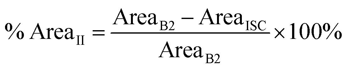 | (5) |
The percentage of VII and AreaII as a function of Δx is presented in Fig. 3f and g, respectively. Even though both values decrease with increasing overlap, the ratio between % VII and % AreaII increases (Fig. 3h). This indicates that smaller separation leads to a greater height in the second blister, observed as a bulging/squeezing effect. These results suggest that further decrease of Δx would lead to even more pronounced bulging.
The optical forging concept can be further expanded. In Fig. 4, trimer formation is presented. The third laser exposure was located in the center of the previously created dimer. Third laser exposure does not affect formerly created blisters, which can be seen in the horizontal cross-section. The profiles of the exterior blisters are unchanged. The bulging effect of the third blister can be observed in vertical and horizontal cross-sections when Δx = 1.0 μm.
 | ||
| Fig. 4 Illustration of trimer overlap with third exposure in the centre of a dimer. AFM images of an optically forged trimer with images of dimers and single blisters used for comparison. Blisters were prepared with 60 pJ pulse energy. Irradiation times are shown in the figure. Order of irradiation is marked in the schemes. Colour gradient from −15 to 35 nm. Scale bar 1 μm. Cross-sections of patterns formed under different experimental conditions are presented. Vertical cross-sections were collected in the position indicated by a colour coded arrow. | ||
The schematic illustration of a tetramer created with varying beam separation distances is presented in scheme I in Fig. 5. Each blister was irradiated for 10 s per spot. Topography measurements for experimentally obtained patterns together with collected nanomechanical properties are shown in Fig. 5a to e. The four-step irradiation with 2 μm separation between facing blisters reveals that adhesion and stiffness were modified beyond the blister area (see red arrows in Fig. 5c and e). When the beam separation gets smaller, the forged blisters start to overlap, following the rule of not changing the overall shape of the previously created blister. However, its nanomechanical properties can be changed. For example, when Δx = 0.6 μm, the central part of the firstly forged blister became less rigid in comparison to the remaining forged shape. This is visible as a blue center on the DMT modulus channel, pointed with a pink arrow in Fig. 5e. This could be related to the different defect concentration over the area exposed to multiple irradiation or increased stress accumulation in the material.
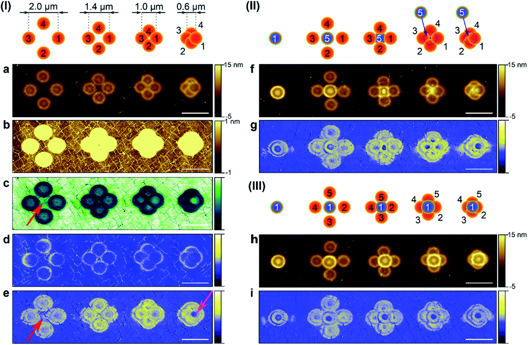 | ||
| Fig. 5 Schemes I–III present complex patterning with marked order of irradiation. In schemes I and II, blisters with 10 s exposure per spot (orange circles) were prepared first. In scheme III, a blister with longer exposure was irradiated first (60 s, blue circle). All blisters were prepared with 60 pJ pulse energy. Topography AFM images of obtained patterns with (a, f and h) full and (b) reduced colour scale, and corresponding (c) adhesion, (d) deformation and (e, g and i) DMT modulus data. Scale bar 2 μm. Red arrows point at changes in adhesion and DMT modulus channels which occur between irradiated spots. Pink arrow points at reduced rigidity over the firstly created blister. | ||
The fifth irradiation for 60 s in the center of the created tetramer is presented in Fig. 5f and schematically presented in scheme II. When the distance between the first and third exposures, Δx1–3, is 2 μm, the fifth blister looks as if it does not overlap with anything. Further decrease in beam separation produces a peculiar pattern. An increasing overlap confines the fifth blister to the remaining small area of pristine graphene and the outer side of the earlier forged blisters. This corresponds to the blister part which shows the highest deformation. For Δx1–3 of 1.4 and 1.0 μm, the created pattern in the center of the tetramer does not exhibit a ring shape, but it adjusts to the available free space. Further decreasing the distance between the spots leads to forging over the central part of the first blister, which was shown to be less stiff. On the other hand, when the first blister was irradiated for 60 s (scheme III and corresponding pattern in Fig. 5h), the consecutive four laser exposures did not change its volume expansion, even when the overlap between the first and the fifth blister becomes significant. A comparison of all collected AFM data is presented in Fig. S7.† These findings show how crucial the suitable choice of exposure order is, as well as the position of the laser beam in creation of a desired 3D structure.
In Fig. 6a we present optical forging following pre-programmed irradiation pathways along x and y directions. We tested three scanning directions: bidirectional, inside-out and outside-in, for which schematic illustrations are presented in Fig. 6a. Inside-out and outside-in pathways follow the squared spiral shape in the clockwise and counterclockwise direction, respectively. By decreasing the horizontal (Δx) and vertical (Δy) spacing between laser spots, the overlap between them increases in all writing pathways. A higher overlap leads to multiple exposures over the intersecting area.
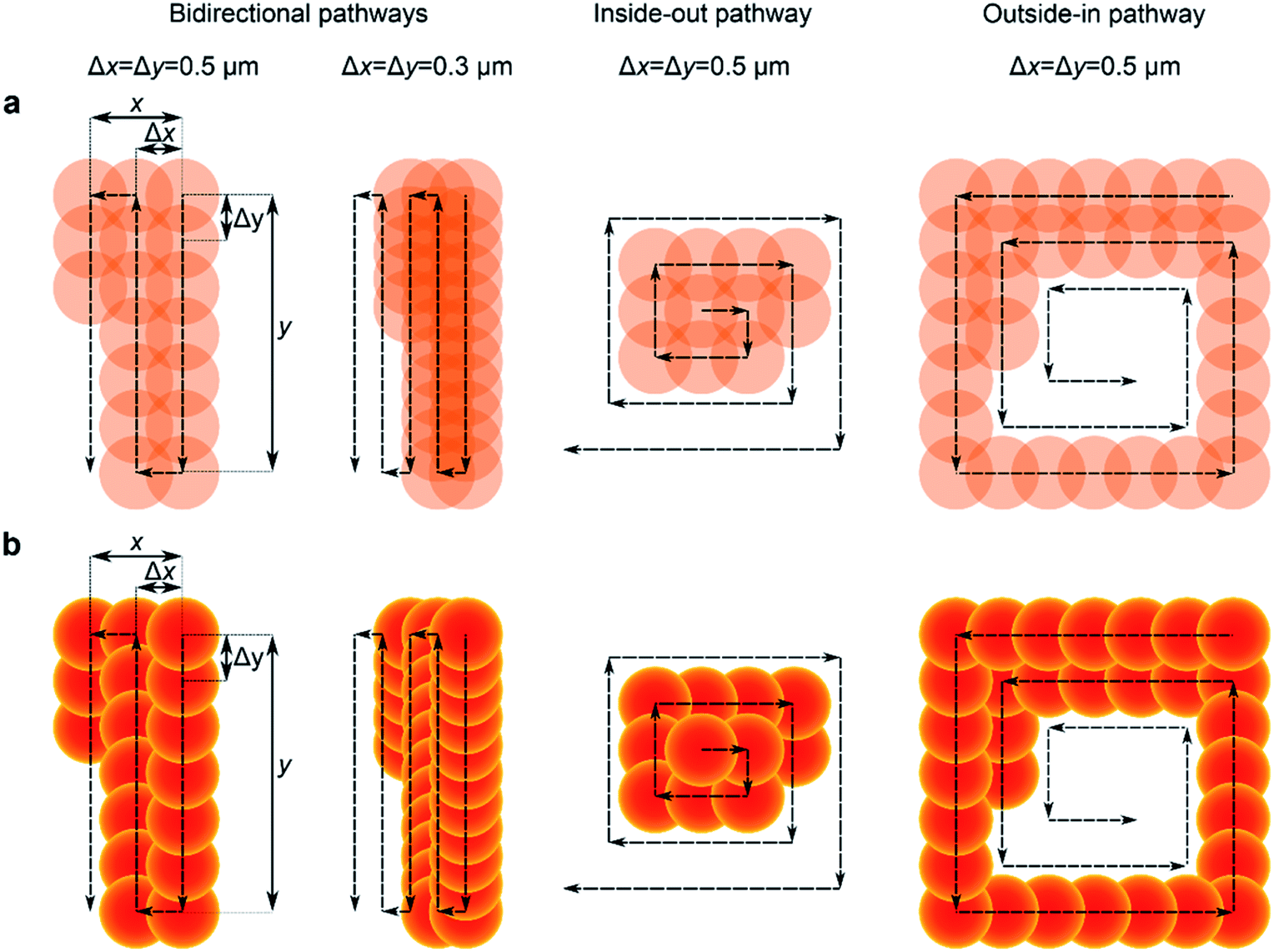 | ||
| Fig. 6 (a) Illustration of focused laser beam positions during optical forging with the beam following bidirectional, inside-out and outside-in pathways, with equal horizontal (Δx) and vertical (Δy) spacing between laser spots. Arrows indicate the direction of optical forging. The accumulation of dose occurs in the intersecting beam area. (b) Illustration of patterns created with a ring-like blister with D = 0.8 μm for pathways and separation distance as in (a). Each new blister is created without changing the profile of the previously created structure. Yellow colour indicates a higher part of the blister. | ||
The gained knowledge of blister formation and dimer overlap allowed us to predict the shape of more complex patterns. The schematic illustrations of the predicted patterns following the pre-programmed laser pathway are presented in Fig. 6b. The patterns were formed by overlapping multiple circles that mimic the shape of a single blister formed by chosen irradiation dose. Blister overlaps were done by considering that consecutive laser exposure does not change the profile of already existing blisters. Hence, in design each new spot ‘hides’ below the previously forged blisters. Larger blisters will produce larger overlap, causing changes in the outcome of the pattern. The prediction is that the shape of sub-diffraction features closely depends on the laser scan direction and separation between the laser spots.
A proof of principle of creating versatile 3D patterns is presented in Fig. 7. We prepared 3 sets of 4 patterns (x = y = 3 μm), each following a different writing path: bidirectional, inside-out or outside-in. Patterns were created using 100 pJ pulse energy and 10 s irradiation time per spot. Each shape was formed with constant laser spot separation Δx = Δy, which was set between 1 μm and 0.1 μm. The optically forged patterns fully resemble the predicted designs. Large step size formed single blisters, which are building blocks for the bigger structure. By decreasing the step size (Δx = Δy = 0.3; 0.5 μm), partial overlap of the blisters was obtained. The idea of a blister not building up over previously formed blisters is beyond doubt visible in experimentally obtained 3D structures. We were also able to write patterns with feature sizes much below the diffraction limit. Patterns created with different irradiation times and pulse energies are presented in Fig. S8 and S9,† respectively. Longer irradiation times create taller structures with more pronounced sharp features. The highest used overlap (Δx = Δy = 0.1 μm) exhibits pronounced bulging effects which allowed us to form elevated, flat-top 3D shapes. The height of the structures can be controlled by the laser dose.21 A square plateau, bulging to the height of 70 nm, was formed with a bidirectional pathway and 0.1 μm separation distance, consisting of 961 highly overlapping laser spots. This shows that low pulse fluences used in optical forging allow a 3D texturing of the irradiated surface instead of removing it, even when a high spatial density of laser exposures is used. This is in contrast to the traditional micromachining, where multiple exposures over the same area usually trigger lowering of the modification threshold. As a consequence, this yields a faster ablation over the intersecting area.42
 | ||
| Fig. 7 Predicted shapes (left) and AFM images of optically forged patterns (right) created by following bidirectional, inside-out and outside-in writing pathways. Patterns were prepared with 100 pJ pulse energy and 10 s irradiation time per spot. The horizontal and vertical separations between laser spots were constant, Δx = Δy = 0.1; 0.3; 0.5 and 1 μm. Scale bar 1 μm. | ||
The writing direction plays a crucial role in pattern formation and shaping of sub-micrometer features. Patterns produced by the outside-in pathway follow shape predictions, however, their central parts exhibit lower heights than the patterns created by other routes. Perhaps it is due to the changing strain conditions of the enclosed graphene surface, resulting in a modified optical forging rate.
The geometrical structure for larger Δx may seem similar to the patterns prepared by typical micromachining, however this is misleading. For example, complex two-dimensional patterning could be compared with the production of amorphous micro-structures in crystalline Si wafer.43 There the structures are formed slightly below the non-irradiated surface. They are created by melting and consecutive solidification with a small fraction of the material evaporating. Most of the traditional micromachining processes are focused on material removal, and therefore holes are produced. In our case we fabricate elevated blisters using low fluences.
Patterning by optical forging can be scaled up. In Fig. 8a and b we present AFM height images of the larger periodic patterns created with spot separation Δx = Δy = 0.5 μm using bidirectional and inside-out irradiation pathways, respectively. The 3D perspective of zoomed regions of optically forged structures is presented in Fig. 8c and d. The repeatable patterns with the same separation of 0.5 μm are observed, with sub-diffraction limited features exhibiting FWHM = 170 nm and FWHM = 110 nm for bidirectional and inside-out pathways, respectively (Fig. 8e and f).
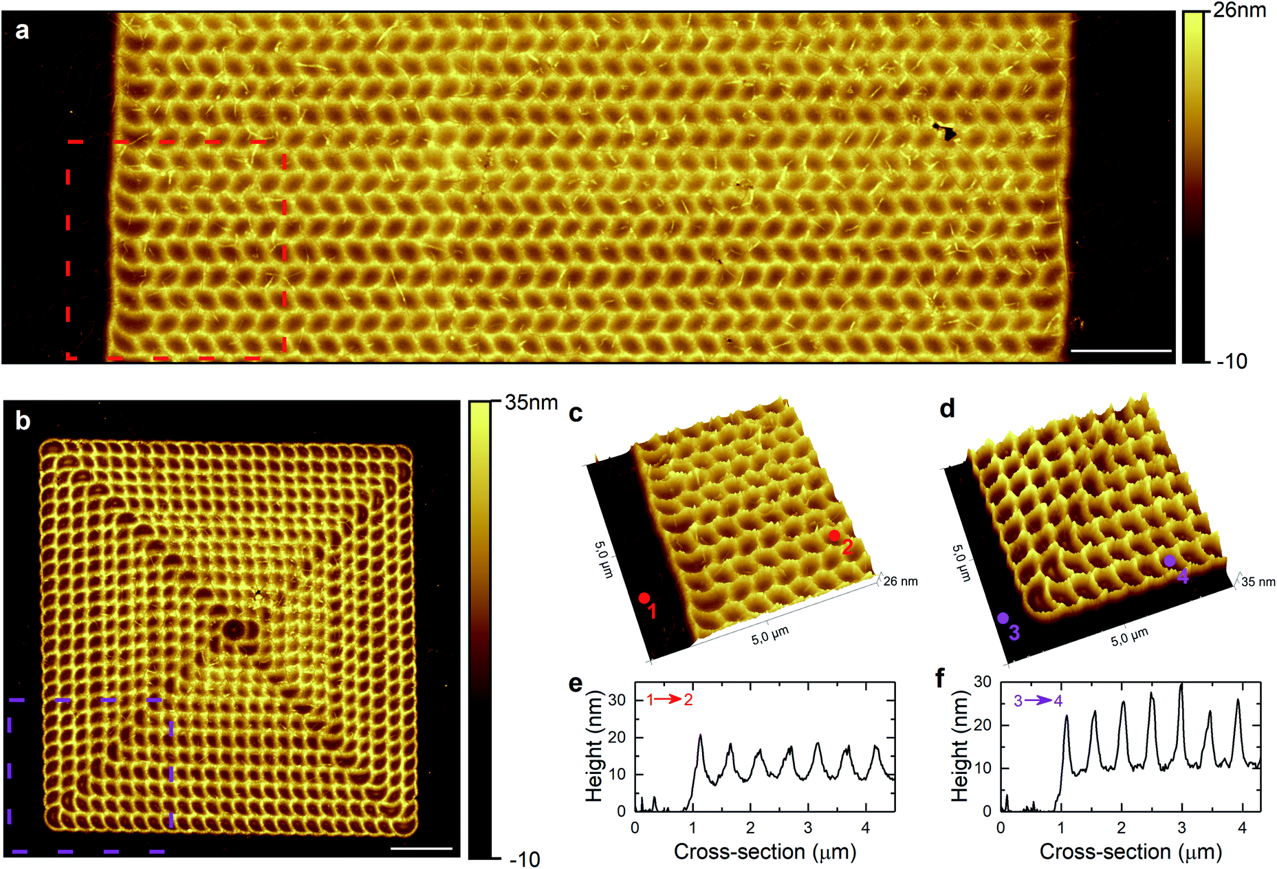 | ||
| Fig. 8 AFM height images of optically forged graphene prepared with a Δx = Δy = 0.5 μm separation distance between laser spots. Patterns were prepared using 80 pJ pulse energy and (a) the bidirectional pathway with 30 s irradiation time per spot and (b) the inside-out pathway with 60 s irradiation time per spot. Scale bar 2 μm. 3D image of the zoomed area marked by dashed (c) red and (d) purple frames. Cross-section measured between points (e) 1–2 and (f) 3–4. | ||
We observed that 3D shaping of bilayer/multilayer graphene is also possible using optical forging (data not shown).
Conclusions
We have demonstrated a reproducible, mask-free method to pattern graphene using femtosecond laser pulses. Using low peak fluences we textured the graphene surface without either ablating it or deforming the underlying Si/SiO2 substrate. We have shown that the well-established micromachining equations used in ablation studies can be used to calculate the modification threshold and incubation coefficient for 3D shaped graphene, fabricated using optical forging. Single pulse modification threshold fluence was estimated to 8.3 mJ cm−2, which is an order of magnitude smaller than the single-pulse ablation thresholds for graphene and 100 nm SiO2 on the Si substrate.Direct laser writing also changes the mechanical properties of the irradiated regions such as adhesion and stiffness. The choice of exposure parameters (e.g. pulse energy, irradiation time) controls the level of material modification and shape of created blisters. We showed that knotty patterns can be designed and then experimentally obtained by controlling:
(a) size of the blister created with a specific laser dose,
(b) separation distance between consecutive laser spots,
(c) the irradiation pathway, following the rule of thumb that each new laser exposure will not change the overall shape of previously formed patterns. Our findings indicate that beam shaping would lead to even more complex 3D pattern formations. Optical forging has great potential for strain engineering of graphene, and possibly other atomically-thin materials.22 It may be a method to shape nanomaterials for applications such as nanoscale scaffolds, novel microelectromechanical systems (MEMS),44 quantum emitters,45 trapping of surface plasmons,46 and use in plasmonic field enhancement.47,48
Conflicts of interest
There are no conflicts to declare.Acknowledgements
V.-M. H. acknowledges funding from the Finnish Cultural Foundation. M. P. acknowledges funding from the Academy of Finland (grant 311330).Notes and references
- R. R. Gattass and E. Mazur, Nat. Photonics, 2008, 2, 219–225 CrossRef CAS.
- Y.-L. Zhang, Q.-D. Chen, H. Xia and H.-B. Sun, Nano Today, 2010, 5, 435–448 CrossRef CAS.
- G. H. Han, S. J. Chae, E. S. Kim, F. Güneş, I. H. Lee, S. W. Lee, S. Y. Lee, S. C. Lim, H. K. Jeong, M. S. Jeong and Y. H. Lee, ACS Nano, 2011, 5, 263–268 CrossRef CAS.
- J. Lu, J. H. Lu, H. Liu, B. Liu, K. X. Chan, J. Lin, W. Chen, K. P. Loh and C. H. Sow, ACS Nano, 2014, 8, 6334–6343 CrossRef CAS.
- A. Venkatakrishnan, H. Chua, P. Tan, Z. Hu, H. Liu, Y. Liu, A. Carvalho, J. Lu and C. H. Sow, ACS Nano, 2017, 11, 713–720 CrossRef CAS.
- V. Shautsova, S. Sinha, L. Hou, Q. Zhang, M. Tweedie, Y. Lu, Y. Sheng, B. F. Porter, H. Bhaskaran and J. H. Warner, ACS Nano, 2019, 13, 14162–14171 CrossRef CAS.
- G. Kalita, L. Qi, Y. Namba, K. Wakita and M. Umeno, Mater. Lett., 2011, 65, 1569–1572 CrossRef CAS.
- W. Zhang, L. Li, Z. B. Wang, A. A. Pena, D. J. Whitehead, M. L. Zhong, Z. Lin and H. W. Zhu, Appl. Phys. A, 2012, 109, 291–297 CrossRef.
- R. Sahin, S. Akturk and E. Simsek, Appl. Phys. A, 2014, 116, 555–560 CrossRef CAS.
- R. Sahin, E. Simsek and S. Akturk, Appl. Phys. Lett., 2014, 104, 053118 CrossRef.
- T. Dong, M. Sparkes, C. Durkan and W. O'Neill, J. Laser Appl., 2016, 28, 022202 CrossRef.
- A. Gil-Villalba, R. Meyer, R. Giust, L. Rapp, C. Billet and F. Courvoisier, Sci. Rep., 2018, 8, 14601 CrossRef CAS.
- E. J. Richman, Y.-T. Chou, Y. Deng, L. Kaelbling, Z. Liang, G. McAlaine, C. Miller, M. Selesnick, C. N. LaFratta and P. Cadden-Zimansky, Opt. Mater. Express, 2019, 9, 3871–3877 CrossRef CAS.
- B. Wetzel, C. Xie, P.-A. Lacourt, J. M. Dudley and F. Courvoisier, Appl. Phys. Lett., 2013, 103, 241111 CrossRef.
- V. Strong, S. Dubin, M. F. El-Kady, A. Lech, Y. Wang, B. H. Weiller and R. B. Kaner, ACS Nano, 2012, 6, 1395–1403 CrossRef CAS.
- J. Koivistoinen, L. Sládková, J. Aumanen, P. Koskinen, K. Roberts, A. Johansson, P. Myllyperkiö and M. Pettersson, J. Phys. Chem. C, 2016, 120, 22330–22341 CrossRef CAS.
- A. Johansson, H.-C. Tsai, J. Aumanen, J. Koivistoinen, P. Myllyperkiö, Y.-Z. Hung, M.-C. Chuang, C.-H. Chen, W. Y. Woon and M. Pettersson, Carbon, 2017, 115, 77–82 CrossRef CAS.
- M. F. El-Kady and R. B. Kaner, ACS Nano, 2014, 8, 8725–8729 CrossRef CAS.
- A. Johansson, P. Myllyperkiö, P. Koskinen, J. Aumanen, J. Koivistoinen, H.-C. Tsai, C.-H. Chen, L.-Y. Chang, V.-M. Hiltunen, J. J. Manninen, W. Y. Woon and M. Pettersson, Nano Lett., 2017, 17, 6469–6474 CrossRef CAS.
- P. Koskinen, K. Karppinen, P. Myllyperkiö, V.-M. Hiltunen, A. Johansson and M. Pettersson, J. Phys. Chem. Lett., 2018, 9, 6179–6184 CrossRef CAS.
- V.-M. Hiltunen, P. Koskinen, K. K. Mentel, J. Manninen, P. Myllyperkiö, A. Johansson and M. Pettersson, J. Phys. Chem. C, 2020, 124, 8371–8377 CrossRef CAS.
- Z. Dai, L. Liu and Z. Zhang, Adv. Mater., 2019, 31, 1805417 CrossRef CAS.
- J. W. Suk, A. Kitt, C. W. Magnuson, Y. Hao, S. Ahmed, J. An, A. K. Swan, B. B. Goldberg and R. S. Ruoff, ACS Nano, 2011, 5, 6916–6924 CrossRef CAS.
- J. M. Liu, Opt. Lett., 1982, 7, 196–198 CrossRef CAS.
- Y. Jee, M. F. Becker and R. M. Walser, J. Opt. Soc. Am. B, 1988, 5, 648–659 CrossRef CAS.
- P. Mannion, J. Magee, E. Coyne, G. O'Connor and T. Glynn, Appl. Surf. Sci., 2004, 233, 275–287 CrossRef CAS.
- F. Di Niso, C. Gaudiuso, T. Sibillano, F. P. Mezzapesa, A. Ancona and P. M. Lugarà, Opt. Express, 2014, 22, 12200 CrossRef.
- A. Rosenfeld, M. Lorenz, R. Stoian and D. Ashkenasi, Appl. Phys. A, 1999, 69, 373–376 CrossRef.
- D. M. A. Mackenzie, J. D. Buron, P. R. Whelan, B. S. Jessen, A. Silajdźić, A. Pesquera, A. Centeno, A. Zurutuza, P. Bøggild and D. H. Petersen, 2D Mater., 2015, 2, 045003 CrossRef.
- A. Roberts, D. Cormode, C. Reynolds, T. Newhouse-Illige, B. J. LeRoy and A. S. Sandhu, Appl. Phys. Lett., 2011, 99, 051912 CrossRef.
- A. Vasquez, P. Samolis, J. Zeng and M. Y. Sander, OSA Continuum, 2019, 2, 2925–2934 CrossRef CAS.
- H. O. Jeschke, M. E. Garcia and K. H. Bennemann, Phys. Rev. Lett., 2001, 87, 015003 CrossRef CAS.
- T. Rublack and G. Seifert, Opt. Mater. Express, 2011, 1, 543–550 CrossRef CAS.
- J. Bonse, S. Baudach, J. Krüger, W. Kautek and M. Lenzner, Appl. Phys. A, 2002, 74, 19–25 CrossRef CAS.
- J. P. McDonald, V. R. Mistry, K. E. Ray, S. M. Yalisove, J. A. Nees and N. R. Moody, Appl. Phys. Lett., 2006, 88, 153121 CrossRef.
- J. Sladek and I. M. Mirza, MM Sci. J., 2019, 2019, 3579–3584 CrossRef.
- J. Thorstensen and S. Erik Foss, J. Appl. Phys., 2012, 112, 103514 CrossRef.
- B. V. Derjaguin, V. M. Muller and Y. P. Toporov, J. Colloid Interface Sci., 1975, 53, 314–326 CrossRef CAS.
- W.-K. Lee, J. Kang, K.-S. Chen, C. J. Engel, W.-B. Jung, D. Rhee, M. C. Hersam and T. W. Odom, Nano Lett., 2016, 16, 7121–7127 CrossRef CAS.
- D. G. Kvashnin and P. B. Sorokin, J. Phys. Chem. Lett., 2015, 6, 2384–2387 CrossRef CAS.
- A. Zandiatashbar, G.-H. Lee, S. J. An, S. Lee, N. Mathew, M. Terrones, T. Hayashi, C. R. Picu, J. Hone and N. Koratkar, Nat. Commun., 2014, 5, 3186 CrossRef.
- S. Xiao, E. L. Gurevich and A. Ostendorf, Appl. Phys. A, 2012, 107, 333–338 CrossRef CAS.
- Y. Fuentes-Edfuf, M. Garcia-Lechuga, D. Puerto, C. Florian, A. Garcia-Leis, S. Sanchez-Cortes, J. Solis and J. Siegel, Appl. Phys. Lett., 2017, 110, 211602 CrossRef.
- X. Fan, A. D. Smith, F. Forsberg, S. Wagner, S. Schröder, S. S. A. Akbari, A. C. Fischer, L. G. Villanueva, M. Östling, M. C. Lemme and F. Niklaus, Microsyst. Nanoeng., 2020, 6, 17 CrossRef CAS.
- C. Palacios-Berraquero, D. M. Kara, A. R. P. Montblanch, M. Barbone, P. Latawiec, D. Yoon, A. K. Ott, M. Loncar, A. C. Ferrari and M. Atatüre, Nat. Commun., 2017, 8, 15093 CrossRef CAS.
- D. Smirnova, S. H. Mousavi, Z. Wang, Y. S. Kivshar and A. B. Khanikaev, ACS Photonics, 2016, 3, 875–880 CrossRef CAS.
- M. Miscuglio, D. Spirito, R. P. Zaccaria and R. Krahne, ACS Photonics, 2016, 3, 2170–2175 CrossRef CAS.
- K. Agarwal, C. Dai, D. Joung and J.-H. Cho, ACS Nano, 2019, 13, 1050–1059 CAS.
Footnote |
| † Electronic supplementary information (ESI) available: Optical forging reproducibility example; cross-sections of blisters and their Raman characterization; AFM nanomechanical data for blisters, tetramers and pentamers; O2 plasma etching data; and AFM height images of complex patterns prepared under various irradiation conditions. See DOI: 10.1039/d0na00832j |
| This journal is © The Royal Society of Chemistry 2021 |