
 Open Access Article
 This Open Access Article is licensed under a Creative Commons Attribution-Non Commercial 3.0 Unported Licence
Low-temperature electronic transport of manganese silicide shell-protected single crystal nanowires for nanoelectronics applications†
Alexsandro dos Santos E. da
Cruz
 *a,
Marcos V.
Puydinger dos Santos
a,
Raul B.
Campanelli
a,
Pascoal G.
Pagliuso
a,
Jefferson
Bettini
b,
Kleber R.
Pirota
a and
Fanny
Béron
a
*a,
Marcos V.
Puydinger dos Santos
a,
Raul B.
Campanelli
a,
Pascoal G.
Pagliuso
a,
Jefferson
Bettini
b,
Kleber R.
Pirota
a and
Fanny
Béron
a
aInstitute of Physics Gleb Wataghin (IFGW), University of Campinas (UNICAMP), Campinas, 13083-859 São Paulo, Brazil. E-mail: asec@ifi.unicamp.br
bBrazilian Center for Research in Energy and Materials (CNPEM), Brazilian Nanotechnology National Laboratory (LNNano), Campinas, 13085-903 São Paulo, Brazil
First published on 19th April 2021
Abstract
Recently, core–shell nanowires have been proposed as potential electrical connectors for nanoelectronics components. A promising candidate is Mn5Si3 nanowires encapsulated in an oxide shell, due to their low reactivity and large flexibility. In this work, we investigate the use of the one-step metallic flux nanonucleation method to easily grow manganese silicide single crystal oxide-protected nanowires by performing their structural and electrical characterization. We find that the fabrication method yields a room-temperature hexagonal crystalline structure with the c-axis along the nanowire. Moreover, the obtained nanowires are metallic at low temperature and low sensitive to a strong external magnetic field. Finally, we observe an unknown electron scattering mechanism for small diameters. In conclusion, the one-step metallic flux nanonucleation method yields intermetallic nanowires suitable for both integration in flexible nanoelectronics as well as low-dimensionality transport experiments.
Introduction
Metallic nanowires have been suggested as building blocks in areas such as non-volatile memory,1 optoelectronics,2,3 flexible and stretchable electronic devices,2–5 nanomedicine,6–8 and nanoelectronics.2,3,9 In the latter case, they are promising candidates to replace indium-tin oxide (ITO) conducting electrodes.10 Despite the widespread technological application of these electrodes, such as touch screens and displays, some shortcomings impair their application for the newest technological trends such as flexible devices. Since the main concern is their brittle nature, Ag and Cu nanowires were considered to overcome this issue based on their good flexibility.11 However, the scarcity and high costs make the Ag nanowire large scale use unviable,2 whereas Cu nanowires are highly reactive in oxidizing environments rapidly compromises their conductivity.12 To ensure stable performance, Won et al. have reported a two-step technique for synthesizing oxidation-resistant Cu@AZO (aluminum-doped zinc oxide) nanowires, which have shown high conductivity, flexibility, and transparency.13 However, their fabrication process requires an additional step of lactic acid treatment for removing the oxide shell from the nanowires, preventing scalable industrial production.Another promising nanowire composition is Mn5Si3, a silicon-based intermetallic compound that exhibits some ceramic properties such as chemical inertness favoring stability in harsh environments required for nanocables.14,15 As it is commonly observed for other silicide nanowires, Mn5Si3 is expected to be a metallic conductor, while integrable into silicon-based devices. Sun et al. have demonstrated that a SiO2 protective layer around long Mn5Si3 nanocables allows conduction under high temperatures, in acidic, or oxidizing environments and permits good system flexibility without creating defects that would degrade their electrical performance.9
In the bulk form, this alloy presents a complex magnetic structure exhibiting two transitions: a non-collinear antiferromagnetic phase transition (AF1) at T1 ≈ 65 K, followed by a collinear one (AF2) occurring at T2 ≈ 105 K.16–18 Both transitions arise from crystallographic phase transitions: expanded orthorhombic to regular (AF1), until hexagonal (AF2). Due to its itinerant electron character, the Mn5Si3 compound electronic behavior is expected to be strongly influenced by its magnetic order, which is anisotropic below T2. Indeed, Vinokurova et al. have found a strong anisotropic resistivity behavior of Mn5Si3 single crystals by applying a current along the c-axis and in the hexagonal basal plane, the latter exhibiting a stronger non-monotonic temperature evolution.19 Besides, reducing the system dimensions can interplay with the magnetic transitions. For example, Sürgers et al.20 have shown that the AF1 and AF2 transitions are less pronounced in a low dimensionality (2D) 160 nm-thick layer, regarding the bulk counterpart.
Nowadays, the common method to grow manganese silicide nanowires is metal–organic chemical vapor deposition (MOCVD).9,21,22 MOCVD favors a single crystalline structure, unlike for Mn5Si3 nanorods obtained via solid-state reaction route.23 However, to achieve a core–shell configuration with MOCVD, a two-steps fabrication route is required.9 Moreover, a further additional mechanical removal of the nanocables from the substrate is mandatory. Consequently, simplifying the growth of conductive nanocables with a protective layer while maintaining their large aspect ratio and single crystalline nature is necessary.
In this work, we propose a new fabrication route for high quality oxide-shell-protected Mn5Si3 nanowires, called metallic flux nanonucleation method (MFNN).24 This fabrication technique, which combines the metal flux method with nanoporous alumina templates, has already been successfully employed on the fabrication of several intermetallic nanowires.24–27 It is a versatile and user-friendly method that presents a possible high yield of around millions of nanowires per squared millimeters. Here, this one-step nanowire production technique allowed us to reproducibly fabricate high crystalline quality manganese silicide oxide-coated nanowires with length up to several tens of microns. MFNN directly yields a core–shell structure that is highly desirable for nanoelectronics applications and allows benefiting from the promising electrical, mechanical, and chemical characteristics of the material as nanocables in harsh environments. Furthermore, MFNN results in high quality single crystals. This point is critical for nanostructures exhibiting properties arising from the reduced dimensionality, compared to the bulk. In this work, we focused on the dimension effects introduced by the mesoscopic diameter (d = 180 up to 800 nm) on the nanowire electrical behavior around the previously discussed bulk AFM transitions (temperature T = 2–300 K).
After confirming their core–shell and homogeneous structure through energy dispersive X-ray spectroscopy (EDS), we carried out further structural characterizations (selected-area electron diffraction (SAED) and transmission Kikuchi diffraction (TKD)) to investigate the crystalline quality of the obtained nanowires. We subsequently probed single nanowire resistivity behavior varying both the temperature and external magnetic field. Results show that the MFNN fabrication technique consistently yields nanowires with the necessary structural and electrical characteristics to be used as nanocables. In particular, their electrical behavior exhibits no notable effect under the application of a magnetic field up to 7 T. Additionally, preliminary measurements suggest that the diameter reduction modifies their electrical properties. Indeed, the smallest diameter of 180 nm presents the lowest resistivity at 300 K (275 μΩ cm). Furthermore, our data indicate a change in the resistivity mechanism for temperature above the detected magnon–electron scattering regime. Whereas thicker nanowires switch to a phonon–electron scattering regime, the smallest nanowire exhibits as an unidentified regime. This transformation occurs around 45–55 K, at lower temperature for thinner nanowires. In conclusion, we show that the MFNN technique is a promising fabrication route for diverse intermetallic nanowires to be used for nanoelectronics as well as for the investigation of physical phenomena in reduced dimension structures.
Results and discussion
Core–shell nanowire fabrication
The MFNN relies upon the well-known thermal flux growth28,29 combined with nanoporous alumina templates.30 Thermal flux is a physical fabrication method based on the slow solidification of bulk materials, where the addition of another excess element – the flux – is used to lower the temperature required to melt the compound elements as well as to improve the solution homogeneity through atomic diffusion during the growth. This process is carried out with slow cooling to favor high crystalline quality and large crystals. The flux technique is suitable for most intermetallic compounds. On the other side, the nanoporous alumina structure used consists of a highly compact array of straight and parallel cylindrical pores (diameter of tens to hundreds of nanometers) and several microns long. It is obtained through the anodization of an aluminum piece or thin film. The template material, aluminum oxide, which yields both mechanical rigidity and chemical inertness to the structure, is used as a matrix by filling the pores for the nanowire fabrication. Thereby, the nanoporous alumina template creates confined regions that induce a preferential longitudinal growth during the element solidification.Fig. 1a depicts a scanning electron microscopy (SEM) image of the alumina surface after the MFNN process. The straight and long synthesized nanowires with length reaching up to 70 μm are encountered freely lying on top of the alumina template. Since the template pores are solely mediating the nanowire growth, they remained clean and empty after removing the remaining liquid elements (Fig. 1b). The histograms of the template pore and the nanowire diameter distributions, built based on the SEM images, are presented in Fig. 1c and d, respectively. While the average pore diameter is 170 ± 10 nm, we observe that the nanowire diameter does not directly follow the pore size distribution. Instead, the nanowire diameter is found to be between 85 and 850 nm, yielding large length to diameter aspect ratios from 100 up to 740. Remarkably, even for a diameter well above the largest pore diameter, the produced nanowires exhibit a homogenous shape (see ESI, Suppl. 1†). This fabrication process repeatedly yielded similar results.
 | ||
| Fig. 1 Nanowire morphology. (a) Secondary electron (SE) image of the nanowires (indicated by white arrows) on top of the alumina template surface. (b) Top-view alumina template SE image. (c) and (d) Alumina pore and nanowire diameter distributions, respectively. (e) Transmission electron microscopy (TEM) nanowire bright-field image and (f) zoom showing its core–shell configuration. | ||
A typical overview TEM image of a nanowire transferred to a grid is seen in Fig. 1e, along with a higher magnification of the marked area (Fig. 1f). The images reveal the nanowire core–shell configuration through a contrast difference, which should be related to regions of different densities.
Chemical composition
EDS mapping was done to obtain the core/shell respective chemical composition information (Fig. 2). From the annular dark-field (ADF) reference image (Fig. 2a), it exhibits Mn-Kα1,2, -Lα1 (Fig. 2b) and Si-Kα1,2, -Kβ1 lines (Fig. 2c), as well as O-Kα1,2 (Fig. 2d) and Ga-Kα1,2, -Kβ1, -Lα1 lines (Fig. 2e), which is the metal flux (see also ESI Suppl. 2, Fig. S2†). In order to compare the element position in the structure shown in Fig. 2a, we constructed overly color maps for Mn and Si, Mn, Si, and O as well as Mn, Si, and Ga (Fig. 2f–h). Furthermore, we obtained line cross-sections and relative intensity scans over the cross-section (Fig. 2i and j). Both results confirm a core–shell nanowire configuration. This nanowire chemical structure persists over the whole nanowire length (see ESI, Suppl. 2, Fig. S3–S8†). The EDS mappings suggest a Mn–Si core with a shell consisting of Si, Ga, and O. Indeed, after carefully subtracting the Si characteristic X-ray contribution from the shell (see ESI Suppl. 2, Table S1†), we obtain an average core proportion of 63 and 37 at% for Mn and Si, indicating an Mn-rich core nanowire. However, since the nanowires grow in a supersaturated flux, Ga atoms may incorporate inside the nanowire core. Indeed, Dong et al. have reported the presence of doping inclusions in silicon nanowires synthesized from a dopant-rich melt.31 Further analyses are required to confirm or exclude this possibility in the Mn–Si nanowires produced by MFNN. Regarding the shell composition, it is assumed to be both Ga2O3 and SiO2, as they are the most stable Ga and Si oxides. The investigated nanowire with a 100 nm diameter is covered by an average total of 12 nm thick protective oxide layer: an outer shell of 5 nm of gallium oxide completely wraps around an 8 nm thick silicon oxide layer. Hence, we have achieved oxide-shell-protected long and straight nanowires, which protects them from corrosion and yields good mechanical strength.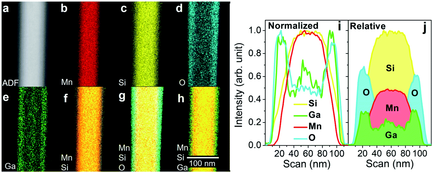 | ||
| Fig. 2 Nanowire core–shell chemical composition. ADF image (a), and EDS maps indicating the presence of Mn-Kα1,2, -Lα1, Si Kα1,2, -Kβ1, O -Kα1,2 and Ga-Kα1,2, -Kβ1, -Lα1 (b)–(e), respectively, with their color mixtures (f)–(h). (i) and (j) Normalized and relative horizontal element intensity scans, obtained from EDS map integration. | ||
Microstructural analysis
We resolved the Mn–Si core crystalline structure and confirmed its stoichiometry using SAED on single nanowires. Experimental SAED data obtained from two zone axes are depicted in Fig. 3a and b, while the simulated ones are presented in Fig. 3c and d, respectively. The SAED results agree with the simulated [320] and [210] zone axes of the Mn5Si3 intermetallic compound assuming a hexagonal crystal structure belonging to the P63/mcm space group. We calculate the lattice parameters to a = b = (6.9 ± 0.3) Å (basal plane) and c = (4.9 ± 0.2) Å, in agreement with literature.32 Furthermore, its c-axis is along the nanowire longitudinal direction, as deduced by the angle comparison between the bright-field TEM image and the [0002] direction in the SAED pattern (Fig. 3e and f, respectively). Finally, SAED performed in three different regions along the nanowire length neither exhibit variations in the diffraction pattern, nor indicates the presence of misorientations (see ESI, Suppl. 3†).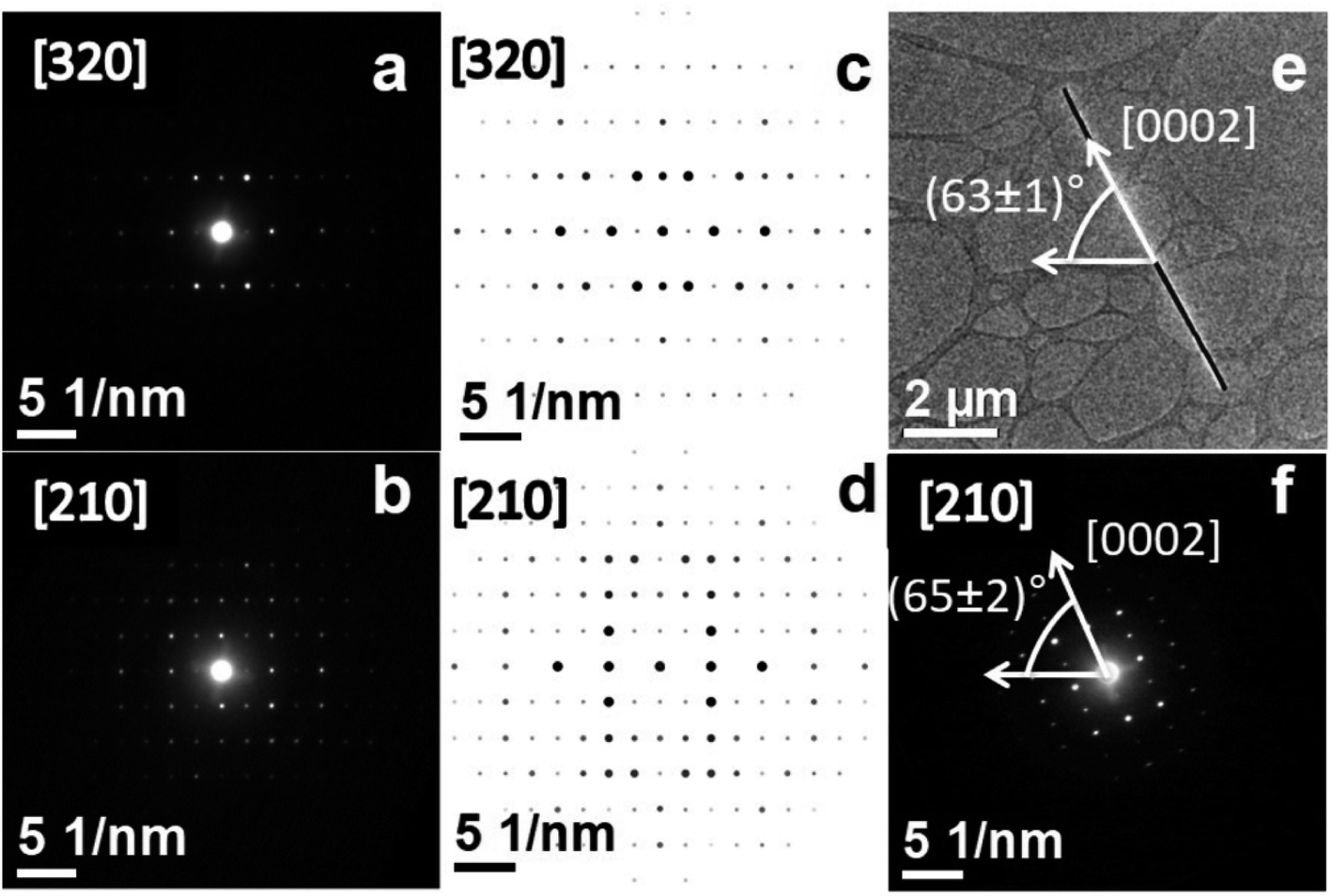 | ||
| Fig. 3 Mn–Si core microstructural SAED analysis (same nanowire than presented in Fig. 2). (a) and (b) Experimental and (c) and (d) simulated SAED patterns for Mn5Si3 crystalline structure. Angle of the nanowire longitudinal direction in the bright-field TEM image (e) and of the [0002] direction in the respective SAED pattern (f). | ||
The nanowire microstructure characterization is completed with transmission Kikuchi diffraction (TKD), a powerful technique sensitive to the grain boundary, size, and orientation, as well as the presence of strain, preferred crystallographic orientation (texture), or crystalline phase distribution.33–36 Remarkably, within the technique resolution, the results indicate none of these aforementioned features, demonstrating the high crystalline quality of the synthesized core–shell nanowires by MFNN (see ESI, Suppl. 4†). Therefore, this new fabrication method turns out to be a promising alternative for achieving oxide-protected nanocables of different compositions for future use in nanoelectronics.
Low-temperature electrical performance
The electrical performance at low temperature of these high-quality single crystal shell-protected nanowires is summarized in Fig. 4. Fig. 4a depicts a resistivity curve as a function of temperature between 2 K and 300 K measuring three single nanowires (diameter d = 180, 450, and 800 nm) in a four-probe setup (see ESI, Supp. 5†). All curves exhibit a monotonically increasing resistivity (ρ) with temperature indicating a metallic behavior. The residual resistivity at 2 K reduces with the nanowire diameter, remaining higher than the bulk value (Table 1). Assuming a similar crystal quality among the nanowires, this dimension-dependent effect may be related to the surface to volume ratio increasing the nanowire surface contribution to the electrical transport. In systems such as oxide-protected InAs nanowires, the oxide layer was identified as reducing the charge mobility due to diffuse boundary scattering.37 Besides, the residual resistivity ratio (RRR = ρ(300 K)/ρ(2 K)) increases with the diameter, reaching values even greater than bulk for d = 450 nm and above (Fig. 4b and Table 1). | ||
| Fig. 4 Single nanowire electrical transport performance. (a) Temperature-dependent resistivity for nanowires of d = 180, 450, 800 nm. (b) Residual resistivity ratio evolution with diameter. Temperature-dependent resistivity with applied magnetic field either perpendicular (c) or parallel (d) to the c-axis (d = 450 nm). | ||
| d (nm) | ρ (μΩ cm) @ 2 K | RRR | T* (K) | ln(A) |
|---|---|---|---|---|
| 180 | 149.5 ± 3.0 | 2.0 | ≈30 | −21.4 ± 0.2 |
| 450 | 109.0 ± 2.2 | 4.3 | ≈45 | −21.4 ± 0.1 |
| 800 | 85.6 ± 4.2 | 4.8 | ≈54 | −21.0 ± 0.2 |
| Bulk19 | 50.0 | 4.0 | — | — |
Furthermore, since sensitivity to external perturbations could impair the nanowire use in nanoelectronic devices, we tested their resistivity robustness under a high magnetic field (H) up to 7 T applied either perpendicular or parallel to the crystallographic c-axis. For all three diameters, we do not detect any notable resistivity change (inside a noise level evaluated to 2%) in the whole temperature range investigated (2–300 K), as shown in Fig. 4c and d for d = 450 nm. This behavior strongly differs from what has been reported in bulk Mn5Si3 single crystals, both on the magnetoresistance and transition temperature aspects. With a current flowing along the c-axis, C. Sürgers et al. have observed a magnetoresistance of 13% at about 52 K, when applying a perpendicular (along the b-axis) magnetic field up to 5 T, together with a T1 decrease.38
Since even the larger diameter nanowires exhibit the same behavior, this discrepancy may not be related to dimensionality effects but rather arising from the different synthesis conditions between the systems. As previously mentioned, the supersaturation melt in which the nanowires are grown may yield an inclusion of Ga atoms in the Mn5Si3 core. On the opposite, no doping is expected in the crystals produced in ref. 38, through a combined Bridgman and flux growth method using Mn self-flux. One hypothesis is that these possible Ga atoms could disturb the crystalline structure, which could modify its magnetic properties. Since the magnetic order strongly depends on the Mn–Mn atomic interactions, it can be altered through external or chemical pressure. In bulk single crystals, L. Vinokurova et al. have reported a T1 shift towards lower temperatures under hydrostatical pressure, before being fully suppressed under pressures around 5.5 kbar.39 B. Gopalakrishnan et al. have observed similar results in Mn5Si3Cx thin films, which have switched from antiferromagnetic to ferromagnetic for x = 0.4.40 Such negative chemical pressure has also been reported in MnSi crystals grown in a Ga flux, induced by the atomic substitution of around 1 at% of Ga atoms at the Si site.41 Therefore, the nanowires synthesized through MFNN might be under chemical pressure due to a Ga doping, to the point in which it either destabilizes the antiferromagnetic coupling or suppresses the AF1 transition, yielding adequate electrical performance for low-temperature application in various environments.
Phase transitions
As previously mentioned, bulk Mn5Si3 undergoes two low-temperature crystalline phase transitions inducing magnetic order modifications. Therefore, based on their high crystalline quality demonstrated by the structural analysis, the nanowires grown by MFNN should be ideal systems to investigate the fundamental phenomena related to these transitions. Above T2 = 105 K, the hexagonal crystalline structure belongs to the P63/mcm space group, where Mn1 occupies an equivalent Si site at 4(d) and Mn2 is located at 6(g) site.32,42 This structure inhibits exchange interaction, leading to a paramagnetic state. When cooling below T2, the crystal develops into an orthorhombic structure, which creates an AFM long-range order collinear along the b-axis.16–18 Finally, this AFM collinearity will be destroyed below T1 = 65 K, due to an expansion of the crystalline structure along the c-axis. Here, we investigate the effects of a unidimensional shape on these low-temperature transitions through resistivity measurements. Further analyses could then relate the resistivity modifications to the structural/magnetic consequences of the unidimensional shape.Several resistivity sources are temperature-dependent, such as electron–phonon, electron–magnon, and electron–electron scatterings, while the residual resistivity, originating from crystalline defects, is constant in temperature. All these terms contribute to the resistivity, adding up according to Matthiessen's rule.43 Regarding phonon scattering, it produces a resistivity evolution Tn at low temperatures that can either be with n = 3 (magnetic compound) or with n = 5 (non-magnetic material), which both reduce to a linear term at high enough temperature.44–46 On the other hand, both antiferromagnetic magnon–electron (for an isotropic system) and electron–electron scatterings yield a resistivity term that is proportional to the squared temperature, T2.44,47,48
From Fig. 4a, we observe that the resistivity curves are qualitatively similar to those obtained from bulk single crystals measured along the c-axis.19 The respective contributions to the electrical resistivity were extracted through their linearization, which exhibits two regions of interest below 90 K (ESI, Supp. 6† and Fig. 5a and b). The results are summarized in Fig. 5c.
 | ||
| Fig. 5 (a) and (b) Linearization process for the 180 nm nanowire. (c) Power laws extracted from the data linearization (error bar represented by the height). (d) Resistivity derivative. | ||
In a first step, we focus on the variation of the transition temperatures between these two resistivity regimes. While there is a net transition for d = 180 and 450 nm, the 800 nm noisier resistivity curve leaves a temperature gap between these regimes (Fig. 5c). Therefore, we opted to define the transition temperature using the resistivity derivative performed after an adjacent-averaging smoothing process (Fig. 5d). We observe that the derivative maximum occurs at a temperature T* either at the linearization transition or inside the temperature interval between the linearized sections. Interestingly, this temperature transition, which may be related to the AF1 bulk transition, increases with the nanowire diameter while remaining below bulk T1 (see Table 1). Several hypotheses may account for the observed trend. On one side, it could be a consequence of the increased proportion of the disordered spins at the surface when increasing the surface to volume ratio. As raised by Kamalakar and co-workers,49 such disordered spins may not support a spin-wave propagation, thus impairing it and favoring a resistivity regime transition at lower temperature. On the other side, remembering that the c-axis coincides with the nanowire one, this expansion may remain sustainable until lower temperature for lower lateral width (i.e. diameter). Probing the temperature evolution of the nanowire magnetization and crystalline structure would help to understand the mechanisms underlying the transition temperature relationship with their dimension.
In a second step, we observe the linearization parameters of the different nanowires (Fig. 5c). In the low-temperature range, all nanowires behave according to an n = 2 mechanism, which arises either from electron–magnon or electron–electron scattering. Similar behavior was reported by Gopalakrishnan et al.40 for a 100 nm-thick polycrystalline Mn5Si3 thin film below 30 K, with a proportionality constant A = 0.6 μΩ cm K−2. They attributed this contribution to magnon–electron scattering, arguing that the resistivity behaviors of the Mn5Si3 and isotropic antiferromagnetic α-Mn compounds are quite similar, the latter having a strong magnon contribution of about 0.1 μΩ cm K−2.44,50 All nanowire A values (≈0.1 μΩ cm K−2) are of the same order of magnitude as those reported in ref. 38 and 44 (see Table 1). Since no diameter dependence is observed, it suggests that a long-range magnetic order occurs in the low-temperature regime for nanowires in the size range investigated.
As the temperature increases, a second regime with a different power law is observed (Fig. 5c). For both larger diameters (d = 450 and 800 nm), the resistivity can be assumed to be linear in this region. This behavior is related to an electron–phonon scattering process, meaning that the lattice vibration contribution becomes preponderant over other resistivity sources. In the interval between T1 and T2, a resistivity increase was also observed for both bulk and thin films of Mn5Si3, but not confirmed as being linear.19,40 However, this trend differs when reducing the diameter until 180 nm. First, the temperature region ends at lower temperature than for larger diameters (52 K vs. 88–90 K, respectively). Moreover, the extracted temperature exponent (n = 1.3 ± 0.1) does not indicate a physical scattering process. Further specific measurements are required to conclude on the consequences of the core–shell nanowire dimensionality reduction in this temperature interval. For example, we already observed a transformation of the magnetic order, from AFM to ferrimagnetic or a mixture of ferromagnetic and AFM, in the intermediary temperature region of Fe3Ga4 nanowires of similar diameter.26
On the other hand, this resistivity contribution modification could explain the smallest nanowire unexpectedly exhibiting the lowest resistivity compared to larger nanowires (see Fig. 4a), especially since it presents the highest residual resistivity and a RRR value less than half than for larger nanowires. From an application point of view, this electrical performance, coupled with a resistivity remaining almost constant for temperatures down to 100 K, yields the d = 180 nm nanowire as the best choice for a nanocable in this temperature range.
Conclusions
Our results show that the MFNN method is suitable to produce high quality, shell-protected, long nanowires. We have successfully synthesized manganese silicide nanowires covered by silicon and gallium oxide layers, which should yield robustness in acidic and oxidizing environments, as already reported in the literature.9 The nanowire Mn5Si3 crystalline structure is free of defects, with a c-axis alignment along the nanowire axis, ensuring optimized electronic transport properties and an ideal platform to investigate emerging physical phenomena in Mn5Si3 nanocrystals. Furthermore, their low-temperature resistivity metallic behavior is robust to external magnetic fields as high as 7 T. This interesting characteristic may arise from a possible Ga doping occurring during the nanowire synthesis in a supersaturated melt. These results corroborate the promising metallic Mn5Si3 nanowires produced by MFNN for the next generation of nanoelectronic devices.By investigating the electron scattering mechanism, we observed that the nanowire diameter reduction to 180 nm modifies the resistivity scattering contributions. At lower temperatures, all investigated nanowires exhibit a magnon–electron contribution. For diameters above 450 nm, it transforms into a phonon scattering mechanism. However, it evolves in an n = 1.3 ± 0.1 behavior for the smallest diameter (180 nm), which does not directly relate to a physical process and may indicate a more complex magnetic order. Remarkably, it presents the lowest resistivity value from 300 K down to 100 K, despite a larger residual resistivity and smaller RRR values than for larger nanowires, as expected. These preliminary observations should be completed by more specific phonon measurements to understand the consequences arising from the diameter reduction. In conclusion, we believe that the metallic flux nanonucleation method is promising for easily producing high quality intermetallic nanowires, either for flexible nanoelectronics or low-dimensionality investigation of emerging physical phenomena.
Materials and methods
Nanowire growth
The Mn5Si3 nanowires were synthesized through the metallic flux nanonucleation (MFNN) technique,24 which combines nanoporous aluminum oxide (Al2O3) templates produced by hard anodization,30 with the standard metallic flux method.28,29 We used Mn, Si, and Ga reagents with purity degrees of 99.98%, 99.999%, and 99.999%, respectively. It is worth mentioning that Ga represents a good flux for these elements since it does not form alloys with Si,51 neither with Mn for concentrations above 75 at% of Ga.52 In this sense, we weighted the reagents in an Mn![[thin space (1/6-em)]](https://www.rsc.org/images/entities/char_2009.gif) :Si:Ga = 1:1:20 proportion. Both the Al2O3 template and the reagents were put into an alumina crucible to be sealed under argon atmosphere in a quartz tube to avoid oxidation during the thermal ramp. After raising the temperature at a 50 °C h−1 rate up to a 1200 °C plateau, which was maintained for 15 hours, it was slowly decreased to 700 °C at a rate of 2 °C h−1. Finally, a spinning process was done to remove the Ga flux excess from the nanoporous template, on top of which the produced nanowires were freely lying.
:Si:Ga = 1:1:20 proportion. Both the Al2O3 template and the reagents were put into an alumina crucible to be sealed under argon atmosphere in a quartz tube to avoid oxidation during the thermal ramp. After raising the temperature at a 50 °C h−1 rate up to a 1200 °C plateau, which was maintained for 15 hours, it was slowly decreased to 700 °C at a rate of 2 °C h−1. Finally, a spinning process was done to remove the Ga flux excess from the nanoporous template, on top of which the produced nanowires were freely lying.
Electron microscopy
The nanowire imaging was performed SEM in a FEI Inspect F50 microscope using the secondary electron mode. To proceed with compositional and microstructural experiments, nanowires were transferred from the Al2O3 template top surface to a carbon grid using a focused ion beam (FIB) Helios 660 manipulator. We used a JEM 2100 F TEM microscope to image the nanowires (bright field), map their composition through EDS (in six areas along the nanowire), and resolve their crystalline structure using SAED (taken in two zone axes in three different regions along the nanowire). On the other side, a FEI Quanta 650 FEG SEM allowed the TKD analysis (with 10 nm resolution), using a thick nanowire (d = 300 nm) to improve the electron inelastic scattering necessary to Kikuchi pattern formation. Subsequently, the pattern was indexed according to the crystalline phase obtained by the SAED analysis.Transport measurements
To perform the transport measurements, the nanowires were transferred onto the platinum electrode in a FIB Helios 660. Inside the chamber, a thinning process was done to remove the oxide layer before the contacts. After being locally exposed to a 30 keV Ga+ beam with 10 pA current, a focused ion-beam-induced deposition (FIBID) of platinum carbon was similarly deposited to achieve an ohmic electrical contact. Further details are available in the ESI, Suppl. 5.† For field/temperature-dependent measurements, the device was carried out in a Quantum Design Physical Properties Measurement System (PPMS) model 6000 with an adapted Keithley 2400 source meter. The four-probe technique was used to avoid contact resistance during the electrical measurements.Conflicts of interest
The authors declare that there is no conflict of interest.Acknowledgements
This work was financially supported by the Brazilian funding agencies Coordenação de Aperfeiçoamento Pessoal de Nível Superior – Brasil (CAPES) – Finance Code 001, Fundação de Amparo à Pesquisa do Estado de São Paulo, FAPESP (Grant number 2017/10581-1) and Conselho Nacional de Desenvolvimento Científico e Tecnológico, CNPq (Grant number 436573/2018-0). We are grateful for the electronic microscopy support from the LNNano – Brazilian Nanotechnology National Laboratory (LNNano/CNPEM/MCTIC) and CCSnano – Semiconductor Components and Nanotechnology Center (UNICAMP). The authors thank Fabiano Montoro, Renan D. Domingos, and Christoph Deneke for the experimental support in the Focused Ion Beam, the resistivity measurements, and the critical manuscript reading, respectively.References
- S. Parkin and S. Yang, Nat. Nanotechnol., 2015, 10, 195–198 CrossRef CAS PubMed.
- H. B. Zeng, J. Z. Song, J. Song and H. Zeng, Angew. Chem., Int. Ed., 2015, 54, 9760–9774 CrossRef PubMed.
- H. G. Im, S. H. Jung, J. Jin, D. Lee, J. Lee, D. Lee, J. Y. Lee, I. D. Kim and B. S. Bae, ACS Nano, 2014, 8, 10973–10979 CrossRef CAS PubMed.
- W. Li, A. Meredov and A. Shamim, npj Flexible Electron., 2019, 3, 19 CrossRef CAS.
- Y. Seo, B. S. Kim, W. C. Ballance, N. Aw, B. Sutton and H. Kong, ACS Appl. Mater. Interfaces, 2020, 12, 13040–13050 CrossRef.
- A. B. A. Nana, T. Marimuthu, P. P. D. Kondiah, Y. E. Choonara, L. C. D. Toit and V. Pillay, Cancers, 2019, 11, 1–23 CrossRef PubMed.
- Y. P. Ivanov, A. Alfadhel, M. Alnassar, J. E. Perez, M. Vazquez, A. Chuvilin and J. Kosel, Sci. Rep., 2016, 6, 1–10 CrossRef PubMed.
- A. I. Martínez-Banderas, A. Aires, S. Plaza-García, L. Colás, J. A. Moreno, T. Ravasi, J. S. Merzaban, P. Ramos-Cabrer, A. L. Cortajarena and J. Kosel, J. Nanobiotechnol., 2020, 18, 1–12 CrossRef PubMed.
- Y. Sun, B. Sun, J. He, G. Yang and C. Wang, Nat. Commun., 2020, 11, 1–8 Search PubMed.
- J. Y. Lee, S. T. Connor, Y. Cui and P. Peumans, Nano Lett., 2008, 8, 689–692 CrossRef CAS PubMed.
- C. F. Guo and Z. Ren, Mater. Today, 2015, 18, 143–154 CrossRef CAS.
- L. Xu, Y. Yang, Z. W. Hu and S. H. Yu, ACS Nano, 2016, 10, 3823–3834 CrossRef CAS PubMed.
- Y. Won, A. Kim, D. Lee, W. Yang, K. Woo, S. Jeong and J. Moon, NPG Asia Mater., 2014, 6, 1–9 Search PubMed.
- X. Chen and C. Liang, Catal. Sci. Technol., 2019, 9, 4785–4820 RSC.
- C. Zou, X. Zhang, G. Jing, J. Zhang, Z. Liao and D. Yu, Appl. Phys. Lett., 2008, 92, 2006–2009 Search PubMed.
- A. Z. Menshikov, A. P. Vokhmyanin and Y. A. Dorofeev, Phys. Status Solidi, 1990, 158, 319–328 CrossRef CAS.
- J. Leciejewicz, B. Penc, A. SzytuŁa, A. Jezierski and A. Zygmunt, Acta Phys. Pol., A, 2008, 113, 1193–1203 CrossRef CAS.
- P. J. Brown, J. B. Forsyth, V. Nunez and F. Tasset, J. Phys.: Condens. Matter, 1992, 4, 10025–10036 CrossRef CAS.
- L. Vinokurova, V. Ivanov, E. Kulatov and A. Vlasov, J. Magn. Magn. Mater., 1990, 90–91, 121–125 CrossRef CAS.
- C. Sürgers, W. Kittler, T. Wolf and H. V. Löhneysen, AIP Adv., 2016, 6, 055604 CrossRef.
- J. M. Higgins, R. Ding and S. Jin, Chem. Mater., 2011, 23, 3848–3853 CrossRef CAS.
- N. binti Hamzan, C. Y. Bin Ng, R. Sadri, M. K. Lee, L.-J. Chang, M. Tripathi, A. Dalton and B. T. Goh, J. Alloys Compd., 2021, 851, 156693 CrossRef.
- L. Wang, J. Lu, J. Zhang, Q. Zhou, Q. Li, W. Liu, Z. Lou and A. Zheng, Micro Nano Lett., 2017, 13, 341–343 Search PubMed.
- K. R. Pirota, K. O. Moura, A. S. E. Cruz, R. B. Campanelli, P. J. Pagliuso and F. Béron, in Magnetic Nano- and Microwires: Design, Synthesis. Properties and applications, ed. M. Vazquez, 2nd edn, 2020, pp. 61–84 Search PubMed.
- P. F. S. Rosa, L. A. S. De Oliveira, C. B. R. De Jesus, K. O. Moura, C. Adriano, W. Iwamoto, T. M. Garitezi, E. Granado, M. E. Saleta, K. R. Pirota and P. G. Pagliuso, Solid State Commun., 2014, 191, 14–18 CrossRef CAS.
- K. O. Moura, L. A. S. De Oliveira, P. F. S. Rosa, C. B. R. Jesus, M. E. Saleta, E. Granado, F. Béron, P. G. Pagliuso and K. R. Pirota, Sci. Rep., 2016, 6, 1–9 CrossRef PubMed.
- K. O. Moura, K. R. Pirota, F. Béron, C. B. R. Jesus, P. F. S. Rosa, D. Tobia, P. G. Pagliuso and O. F. De Lima, Sci. Rep., 2017, 7, 3–9 CrossRef PubMed.
- P. C. Canfield and Z. Fisk, Philos. Mag. B, 1992, 65, 1117–1123 CAS.
- Z. Fisk and J. P. Remeika, in Handbook on the Physics and Chemistry of Rare Earths, 1989, vol. 12, pp. 53–70 Search PubMed.
- W. Lee, R. Ji, U. Gösele and K. Nielsch, Nat. Mater., 2006, 5, 741–747 CrossRef CAS PubMed.
- T. Dong, Y. Sun, Z. Zhu, X. Wu, J. Wang, Y. Shi, J. Xu, K. Chen and L. Yu, Nano Lett., 2019, 19, 6235–6243 CrossRef CAS PubMed.
- R. G. Yusupov, C. J. Stanley, M. D. Welch, J. Spratt, G. Cressey, M. S. Rumsey, R. Seltmann and E. Igamberdiev, Mineral. Mag., 2009, 73, 43–50 CrossRef CAS.
- A. J. Wilkinson and T. Ben Britton, Mater. Today, 2012, 15, 366–376 CrossRef CAS.
- M. Calcagnotto, D. Ponge, E. Demir and D. Raabe, Mater. Sci. Eng., A, 2010, 527, 2738–2746 CrossRef.
- S. D. Sitzman, Testing, Reliab. Appl. Micro- Nano-Material Syst. II, 2004, vol. 5392, p. 78 Search PubMed.
- W. Zhou and Z. L. Wang, Scanning microscopy for nanotechnology: Techniques and applications, 2007 Search PubMed.
- P. Uredat, R. Kodaira, R. Horiguchi, S. Hara, A. Beyer, K. Volz, P. J. Klar and M. T. Elm, Nano Lett., 2020, 20, 618–624 CrossRef CAS.
- C. Sürgers, T. Wolf, P. Adelmann, W. Kittler, G. Fischer and H. V. Löhneysen, Sci. Rep., 2017, 7, 1–7 CrossRef PubMed.
- L. Vinokurova, V. Ivanov and E. Kulatov, Phys. B, 1995, 211, 96–98 CrossRef CAS.
- B. Gopalakrishnan, C. Sürgers, R. Montbrun, A. Singh, M. Uhlarz and H. v. Löhneysen, Phys. Rev. B: Condens. Matter Mater. Phys., 2008, 77, 104414 CrossRef.
- C. Dhital, M. A. Khan, M. Saghayezhian, W. A. Phelan, D. P. Young, R. Y. Jin and J. F. Ditusa, Phys. Rev. B, 2017, 95, 1–8 CrossRef.
- B. Aronsson, D. H. Templeton, S. Rundqvist, E. Varde and G. Westin, Acta Chem. Scand., 1960, 14, 1414–1418 CrossRef CAS.
- M. P. Marder, in Condensed Matter Physics, Wiley, 2nd edn, 2010, pp. 528–529 Search PubMed.
- P. Taylor and G. T. Meaden, Contemp. Phys., 2006, 12, 37–41 Search PubMed.
- A. H. Wilson, Proc. R. Soc. London, Ser. A, 1938, 167, 580–593 CAS.
- W. H. Butler, Phys. Today, 1978, 31, 44–49 Search PubMed.
- D. A. Goodings, J. Appl. Phys., 1963, 34, 1370–1371 CrossRef CAS.
- W. G. Baber, Proc. R. Soc. London, Ser. A, 1937, 158, 383–396 CAS.
- M. V. Kamalakar, A. K. Raychaudhuri, X. Wei, J. Teng, P. D. Prewett, M. V. Kamalakar, A. K. Raychaudhuri, X. Wei and J. Teng, Appl. Phys. Lett., 2009, 95, 013112 CrossRef.
- G. T. Meaden and P. Pelloux-Gervais, Cryogenic, 1965, 5, 227–228 CrossRef CAS.
- R. W. Olesinski, N. Kanani and G. J. Abbaschian, Bull. Alloy Phase Diagrams, 1985, 6, 362–364 CrossRef CAS.
- H. Okamoto, J. Phase Equilib. Diffus., 2014, 35, 105–116 CrossRef CAS.
Footnote |
| † Electronic supplementary information (ESI) available. See DOI: 10.1039/d0na00809e |
| This journal is © The Royal Society of Chemistry 2021 |