
 Open Access Article
 This Open Access Article is licensed under a Creative Commons Attribution-Non Commercial 3.0 Unported Licence
Simultaneous layer exfoliation and defect activation in g-C3N4 nanosheets with air–water interfacial plasma: spectroscopic defect probing with tailored optical properties†
Trishamoni
Kashyap
ab,
Palash J.
Boruah
c,
Heremba
Bailung
c,
Dirtha
Sanyal
 d and
Biswajit
Choudhury
*a
d and
Biswajit
Choudhury
*a
aMaterials and Energy Laboratory, Physical Sciences Division, Institute of Advanced Study in Science and Technology, Paschim Boragaon, Vigyan Path, Guwahati-35, India. E-mail: biswajitchoudhury@iasst.gov.in; biswa.tezu@gmail.com
bDepartment of Physics, Cotton University, Panbazar, Guwahati-01, India
cBasic and Applied Plasma Physics, Physical Sciences Division, Institute of Advanced Study in Science and Technology, Paschim Boragaon, Vigyan Path, Guwahati-35, India
dVariable Energy Cyclotron Centre, HBNI, 1/AF Bidhannagar, Kolkata-700064, India
First published on 1st April 2021
Abstract
Defect-activated ultrathin graphitic carbon nitride nanosheets (g-C3N4) show an enhanced visible light absorption, better charge-separation, and facile charge transport properties. These are requisites for the designing of an active photocatalyst. Conventional methods used for layer exfoliation and defect activation require strong acids, reducing agents, or ultrasonic treatment for a sufficiently long duration. Furthermore, single-step approaches for layer exfoliation and defect incorporation have hardly been reported. Herein, we have shown atmospheric plasma enabled fabrication of g-C3N4 nanosheets. This approach is simple, low-cost, less time-consuming, and a green approach to exfoliate layers and activate multiple defects concurrently. The protocol involves plasma discharging at an air–water interface at 5 kV for 30–150 min. Atomic force microscopy (AFM) reveals a layer thickness of 96.27 nm in bulk g-C3N4. The thickness becomes 3.78 nm after 150 min of plasma treatment. The exfoliated layers emerge with nitrogen-vacancy sites and self-incorporated defects as probed by positron annihilation spectroscopy (PAS) and X-ray photoelectron spectroscopy (XPS). The defect activated layers show visible light absorption extended up to 600 nm. It is demonstrated that a non-uniform change in the band gap with the plasma treatment time results from quantum confinement in thin layers and Urbach tailing due to defects acting in opposition. Further, steady-state and time-resolved spectroscopy shows the contribution of multiple defect sites for a prolonged lifetime of photoinduced carriers. These defect-activated ultrathin nanosheets of CN serve as an active photocatalyst in the degradation of rhodamine B (RhB) under white LED illumination.
1. Introduction
In recent years, graphitic carbon nitride (g-C3N4) has evolved as an excellent two-dimensional (2D) metal-free photocatalyst in water splitting, air and water pollutant removal, and CO2 reduction.1–3 The photocatalytic efficiency of bulk g-C3N4 is constricted by its poor visible-light absorption, fast-carrier recombination and long diffusion paths of photoinduced carriers.3–5 Intrinsic structural modification can help g-C3N4 in overcoming these difficulties. Among the different strategies such as doping, composite and heterojunction formation, structural modifications, defect and facet engineering to modify g-C3N4 suitably for better activity, intrinsic modifications involve layer exfoliation and defect activation.4–8 Exfoliated g-C3N4 nanosheets display much improved and unique electronic and physical properties different from their bulk counterparts.9–11 Some of the distinguishing features are the high surface area, short-diffusion lengths of photoinduced carriers, high electron mobility, and long carrier lifetimes.9,10 Intrinsic defect incorporation into the nanosheets can significantly improve absorption of visible to NIR light, prohibits facile carrier recombination, and provides numerous surface-active sites.8,12 These modifications make g-C3N4 a suitable candidate for areas such as photochemical H2 energy generation, water purification, memory devices, and bio-imaging applications.9–15Conventional methods for layer exfoliation are ultrasonication, chemical, thermal oxidation, etc.8,16 A thermal oxidation method of bulk g-C3N4 results in nanosheets of an average thickness of 2.33 nm. However, the major flaw of this technique is the reasonably low product yield as g-C3N4 decomposes into gaseous products.9 In the solvent-mediated exfoliation process, g-C3N4 is dispersed in solvents such as isopropyl alcohol (IPA), N-methyl-pyrrolidone (NMP), water, ethanol, or acetone, and ultrasonically treated for 10 h. The resultant nanosheets acquire a thickness of 2 nm in propanol.9 In water as a dispersing medium, the ultrasonically exfoliated nanosheets attain a thickness of 2.5 nm.15 The drawback of the ultrasonication process is that it consumes a large amount of time. The chemical exfoliation process involves dipping g-C3N4 in concentrated H2SO4 for a period of 8 h. The process generates ultrathin nanosheets of a thickness of 0.4 nm.9 The waiting time for chemical exfoliation is lengthy and extreme care is required in handling the acids.
Another promising strategy to improve the photocatalytic activity of a 2D layered material like g-C3N4 is the incorporation of defects into the system. A successful defect incorporation into g-C3N4 requires the use of ammonium chloride, NaBH4, KOH, or KSCN, and thermal annealing in an inert atmosphere (H2).5,12,17–20 g-C3N4 enriched with nitrogen and carbon vacancy sites possesses numerous surface reactive sites, show enhanced visible absorption, and improved charge carrier dynamics useful for designing an improved photocatalytic system.
Some of the above-mentioned reports have deliberated on exfoliation of g-C3N4 and some reports focused on the formation of defects. However, a single step process for simultaneous layer exfoliation and defect formation in g-C3N4 is not found in any of these reports. Therefore, herein, for the first time, we have reported application of atmospheric pressure plasma at an air–water interface for simultaneous layer exfoliation and defect generation in g-C3N4 nanosheets.
The air–liquid interfacial plasma adopted here is different from that of plasma-induced etching used for the surface treatment of nanomaterials. Plasma etching requires a low-pressure vacuum chamber inside which the substrate or sample, and an electrode are kept. Plasma is generated on the electrode inside the chamber by a radiofrequency generator. When gases such as O2, N2etc. are purged into the chamber, the gases are ionized. These ionized gases directly bombard the sample surface leading to its etching. For example, Bu et al. used oxygen plasma for introducing a surface N–OH group by oxygen doping.21 Ji et al. used oxygen and nitrogen plasma for surface treatment of g-C3N4.22 While oxygen plasma treatment etches the surface of g-C3N4 and introduces the oxygen functionality, nitrogen plasma treatment remediates nitrogen vacancies present in the sample. Except for surface modification, the plasma treatment does not lead to any layer exfoliation or other morphological changes.21,22 In contrast to these techniques, herein, air–liquid plasma is generated by applying a high voltage of 5 kV in air just above a dispersed solution containing g-C3N4. The air–liquid plasma exfoliation process offers the following advantages in comparison to conventional techniques:
1. It is a green approach as it occurs without the aid of chemicals.
2. A single-step approach leads to both layer exfoliation and defect activation.
3. Unlike an ultrasonication/chemical process, the atmospheric plasma approach requires a reasonably shorter time.
In our study, we have performed positron annihilation spectroscopy (PAS), and X-ray photoelectron spectroscopy (XPS) as probing techniques to identify the incorporated defects in g-C3N4. The ultrathin structure provides a better charge transport through the layers. The incorporated defects enhance visible absorption and serve as charge accumulating sites for facilitating better charge separation, which are ultimate requisites for designing a better photocatalytic system.11,20 Finally, the impact of layer exfoliation and defect activation on the optical transition and charge carrier recombination dynamics is studied with absorption spectroscopy, and steady-state and time-resolved photoluminescence (PL) spectroscopy. Thus, with a reduced layer number, extended absorption and generated vacancies, the air–liquid plasma exfoliated g-C3N4 has promising potential for photocatalytic applications.
2. Experimental
The atmospheric pressure air-plasma reactor consists of two electrodes and a glass beaker containing 40 mg of bulk g-C3N4 (CN) in 100 mL de-ionized water. The stainless-steel electrode (grounded) is submerged in water, while the copper electrode placed at a distance of 2 mm above the water surface is used for plasma generation. For the generation of plasma, a high AC voltage of 5 kV is applied to the copper rod. Plasma is generated for 30 min to 150 min above the liquid surface. During this time, the aqueous dispersion of CN is continuously stirred. The exfoliated products are named CN30, CN60, CN90, CN120, and CN150. The exfoliated nanosheets are separated from unexfoliated CN through centrifugation. Starting with 40 mg of pristine CN, the yield after 30 min plasma-treatment (CN30) is 50–55% (20–22 mg). As the plasma exfoliation time increases, the amount of exfoliated CN nanosheets in the dispersion also increases. Hence, the yield is high for the sample CN150, which is nearly 75% (30 mg). Of note, there was a mass loss of ∼3–5% during recovery of exfoliated nanosheets after centrifugation. The final product after washing is dried in an oven to obtain the exfoliated nanosheets in a powder form.The crystalline structure of the prepared photocatalysts is examined with X-ray diffraction (XRD) in a Bruker D8 Advanced X-ray diffractometer under a Cu Kα X-ray beam of λ = 0.154 nm. An optical emission spectrometer (Andor SR303i-A, fitted with an iDus DV420A-OE CCD detector, focal length: 0.3 m) with a slit width of 100 μm and grating 300 groovesper mm is used to identify the emission of various plasma species. The morphology of the samples is viewed with a transmission electron microscope (TEM, JEOL Ltd.) at an operating voltage of 200 kV. A semi-contact mode atomic force microscope (AFM, NTEGRA Prime) is used for imaging the morphology of the nanosheets. UV-visible diffuse reflectance spectra (DRS) are recorded in a Shimadzu UV-2600 spectrophotometer. The reflectance spectra are recorded by mixing a requisite amount of samples with BaSO4. The reflectance is converted to absorption by following the Kubelka–Munk (KM) function, which is  , where
  . For a positron annihilation spectroscopy (PAS) study, two identical pellets of thickness ∼1 mm and diameter 15 mm are taken to make the sample-source-sample sandwich. In the present experiment, a ∼10 mCi 22NaCl positron source is enclosed in 1.5 mm thick nickel foil. Identical, 12% efficiency, HPGe detectors (PGC 1216sp of DSG, Germany, energy resolution of 1.15 keV at 514 keV of 85Sr radioactive source) were used for the measurements of coincidence Doppler broadening (CDB) spectra of the electron-positron annihilated 511 keV gamma rays. About 107 numbers of coincidence data are recorded for each sample in a dual ADC based – multiparameter data acquisition system (MPA-3 of FAST ComTec, Germany). The standard fast – fast coincidence assembly is constructed using two BaF2 scintillators coupled with XP2020Q photomultiplier tubes as two gamma ray detectors for the measurements of the sub-nanosecond positron annihilation lifetime (PAL). The PAL setup has a lifetime of 200 ps using a 60Co source with an appropriate positron window. X-ray photoelectron spectroscopy (XPS) analysis is carried out in an ESCALAB Xi+ (Thermo Fischer Scientific Pvt. Ltd., UK). The X-ray source Al kα with a pass energy of 50 eV is used for a narrow scan (for individual elements). Photoluminescence (PL) spectra are monitored with a Fluromax-4 spectrometer (Horiba Scientific). Time-resolved photoluminescence (TRPL) spectra are recorded in a picosecond time-resolved luminescence spectrometer (Edinburgh Instruments, model: FSP920).
3. Results and discussion
The experimental set-up is shown in Fig. 1a. The exfoliated products had a slight variation in colour, shown in Fig. 1b. The different ionized species in the plasma and their interaction with the liquid surface are shown schematically in Fig. 1c. Optical emission spectroscopy (OES) detects the presence of N2, N2+, OH, and NO species in the plasma as shown in Fig. 1d, which is in agreement with the previous report.23 | ||
| Fig. 1 (a) Experimental set-up for plasma discharge, (b) colour variation in CN when treated with plasma for different time durations, (c) schematic of different species formed near the air–liquid interface during plasma discharge experiment. The blue line is a symbolic representation of the interface. (d) OES spectrum showing the presence of different plasma-generated species in air. | ||
AFM is taken as a direct tool to measure the size and thickness of the nanosheet after plasma exfoliation, as shown in Fig. 2.
 | ||
| Fig. 2 AFM images of bulk (CN) and plasma-treated samples (CN30, CN60, and CN150) for different time durations (Axis and label colours of CN150 are changed for better contrast). | ||
The lateral size of the nanosheet decreases from 351 nm in CN to 118 nm in CN150. AFM height-profile reveals a reduction in the average thickness from 96.27 nm in bulk CN to 3.78 nm in CN150. This indicates that the plasma exfoliation process successfully separates the layers. Moreover, the reduced lateral size means breaking up of the CN chains at the bridging N atom joining the s-heptazine rings.
The crystallinity of CN is preserved after plasma treatment, as revealed from X-ray diffraction (XRD). There are no noticeable differences in the XRD peak positions between untreated and plasma-treated samples. The pattern records two peaks at 27.7° and 13° corresponding to the (002) and (100) planes, respectively (Fig. 3a). The (002) plane measures the interlayer separation, and the (200) plane measures the separation of the two s-heptazine units of CN.3,24 The TEM images of CN150 are shown in Fig. 3b–d. A nanoflake region in Fig. 3c is taken in a high-resolution mode and is shown in Fig. 3d. As Fig. 3d shows the nanosheets contain nearly 12–13 layers with an interlayer separation of 0.33 nm.
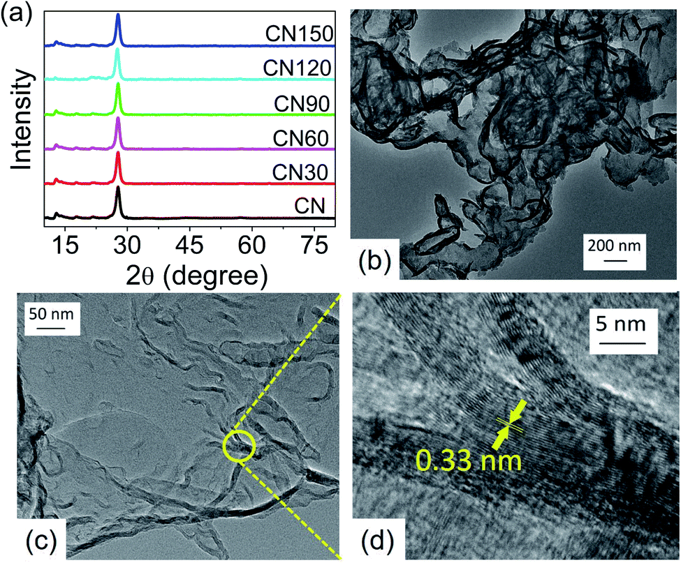 | ||
| Fig. 3 (a) XRD pattern of the samples. The nanoflake like morphology of CN150 is reflected in (b) and (c) in TEM images. A part of (c) is taken in high-resolution mode to observe the stacked layers with an interlayer separation of 0.33 nm (d). | ||
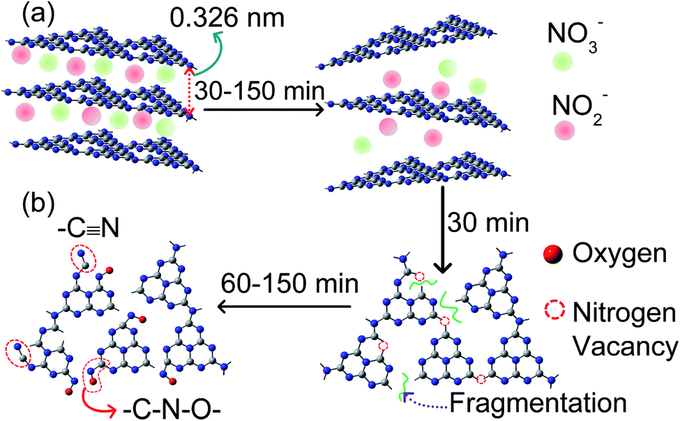
The layer exfoliation process of CN is speculated and discussed with the help of a schematic in Fig. 4. Our OES study and previous report identify the presence of N2, N2+, OH, NO, HNO2, and HNO3 species in the air-discharged plasma.23 These species diffuse from air into water and undergo several reactions. Out of all the diffused species, NO, HNO2 and HNO3 sustain for a sufficiently long duration in water and interact with dispersed CN nanosheets.25 Because of the high reactivity, O2− and OH− ions have a shorter lifetime in water and do not bring any significant changes to the CN nanosheet. Once diffused in water, the plasma-activated electrons, HNO2 and HNO3, undergo the following sequence of reactions:25
 | ||
| Fig. 4 Proposed mechanism for plasma-induced simultaneous (a) exfoliation and (b) defect generation in CN nanosheets. | ||
1. Plasma discharged electrons (eplasma) enter into the aqueous medium and become solvated (esol)
| eplasma + H2O → H + OH + esol |
2. At the interface, the following reactions are initiated by the long-lived species.
| NO + OH → HNO2 |
| NO2 + OH → HNO3 |
3. HNO2 and HNO3, thus formed at the interface, diffuse into the bulk volume and undergo the following set of reactions:
| 2NO2 + 2H2O → NO3− + HNO2 + H3O+ |
| 2NO2 + 3H2O → NO3− + NO2− + 2H3O+ |
The concentrations of NO3− and NO2− species in water are expected to show an increase with time. Since the ionic radii of NO2− (0.192 nm) and NO3− (0.179 nm) are smaller than the interlayer separation in CN (0.33 nm in our analysis),26 these ions readily move into the interlayer gap and intercalate with the layers, as shown in Fig. 4a. The coulombic repulsion between these ions weakens the interlayer interaction of the nanosheets and separates the layers. As the plasma discharging time increases, more and more NO3− and NO2− ions are intercalated, and as a result the exfoliation process gets accelerated. Besides layer exfoliation, there occurs a breaking up of chains, as evident from the decreased lateral size of the nanosheet from AFM. The breaking of the chains is possibly led by a fraction of relatively high-energy (∼10 eV equivalent to 964.8 kJ mol−1) electrons produced in the plasma.27 The energy of these discharged electrons is higher than the bond dissociation energy of bridging C–N (∼458 kJ mol−1) and aromatic C![[double bond, length as m-dash]](https://www.rsc.org/images/entities/char_e001.gif) N (∼573.6 kJ mol−1) bonds.28 The plasma discharged electrons enter into the water and are involved in a series of reactions. Therefore, only a fraction of these electrons directly interact with C–N and CN bonds in g-C3N4 and lead to the breaking of the chains and introduce structural defects. The small fraction of these electrons does not cause structural distortion, as directly evident from the unaltered high crystallinity spectra of the plasma treated samples in XRD. The mechanistic approach of defect generation and defect incorporation is shown in Fig. 4b. The disruption of chains generates nitrogen vacancies (Nv) and leaves many unsaturated carbon dangling bonds. These dangling sites readily bind with NO2− and NO3− ions and form –C–N–O– bonding and –C
N (∼573.6 kJ mol−1) bonds.28 The plasma discharged electrons enter into the water and are involved in a series of reactions. Therefore, only a fraction of these electrons directly interact with C–N and CN bonds in g-C3N4 and lead to the breaking of the chains and introduce structural defects. The small fraction of these electrons does not cause structural distortion, as directly evident from the unaltered high crystallinity spectra of the plasma treated samples in XRD. The mechanistic approach of defect generation and defect incorporation is shown in Fig. 4b. The disruption of chains generates nitrogen vacancies (Nv) and leaves many unsaturated carbon dangling bonds. These dangling sites readily bind with NO2− and NO3− ions and form –C–N–O– bonding and –C![[triple bond, length as m-dash]](https://www.rsc.org/images/entities/char_e002.gif) N bonding, as shown in Fig. 4b.19,29,30
N bonding, as shown in Fig. 4b.19,29,30
The results of AFM support our mechanism for layer exfoliation. However, to probe the generation of vacancies and self-incorporated defects, we pursued PAS and XPS. The types of defects evolved in CN are investigated with PAS. The positron annihilation lifetime parameters are obtained by deconvolution of the positron annihilation lifetime spectrum using computer programme PATFIT-88 with two components fitting (variance of fit < 0.5 per channel).
Typical positron lifetime parameters for the four samples are shown in Table 1. The short lifetime component (τ1) arises from the free annihilation of positrons from the bulk of the sample, while the second positron lifetime (τ2) is due to the annihilation of positrons at the point defect site. The intensity of the second positron lifetime (I2) is a signature of the relative amount of such defects present in the sample. The value of I2 is highest (79 ± 2%) for the sample CN150 suggesting maximum defects present in this particular sample.
| Sample | τ 1 (ps) | I1 (%) | τ 2(ps) | I 2 (%) |
|---|---|---|---|---|
| CN | 155 ± 2 | 31 ± 2 | 234 ± 6 | 69 ± 2 |
| CN30 | 157 ± 2 | 33 ± 2 | 234 ± 5 | 67 ± 2 |
| CN90 | 155 ± 2 | 45 ± 2 | 261 ± 7 | 55 ± 2 |
| CN150 | 156 ± 2 | 24 ± 2 | 231 ± 5 | 79 ± 2 |
Fig. 5a shows the area-normalized coincidence Doppler broadening (CDB) spectra of the samples with an area normalized CDB of 99.9999% pure Al sample.31 The maximum peak intensity corresponds to pL = 11 × 10−3moC, where mo is the rest mass of the electron and c is the velocity of light. Using the relation ε = pL2/2mo, the momentum value of 11 × 10−3moc corresponds to the kinetic energy (K.E.) of the electron of 31 eV, which is very close to the kinetic energy of the 2 s electron of nitrogen ∼37 eV. Thus, the peak at 11 × 10−3moC is because of the annihilation of positrons with the 2 s nitrogen electron.24 In Fig. 5a, CN30 and CN90 show a reduced peak intensity as compared to bulk CN. The peak intensity increases in CN150 and becomes stronger than that of bulk CN. A decrease in the peak intensity suggests the formation of nitrogen-related vacancies. Therefore, from Fig. 5a, we have inferred that CN30 and CN90 have higher numbers of nitrogen vacancies than bulk CN. For a further understanding, we have measured area normalized CDB spectra of plasma-treated samples with respect to bulk CN (Fig. 5b). The graph in Fig. 5b shows a large deep for the sample CN30, which signifies nitrogen open volume defects. At 150 min, the curve is nearly flattening, likely due to the incorporation of new nitrogenated species in the CN structure. Thus, Fig. 5a and b signify the maximum generation of nitrogen vacancies in the CN nanosheet in the first 30 min of plasma treatment. However, as the plasma treatment time increases, self-incorporated nitrogenated groups (defects) fill up these vacancies, which are arguably NO2− and NO3− from water. Because of these self-incorporated defects, we have seen an increase in peak intensity in Fig. 5a, and flattening of the spectrum in Fig. 5b for CN150.
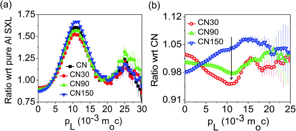 | ||
| Fig. 5 (a) Ratio curves of the area-normalized CDB spectra of pure and plasma-treated samples with respect to 99.9999% pure Al. (b) CDB spectra of plasma-treated samples with respect to pure CN. | ||
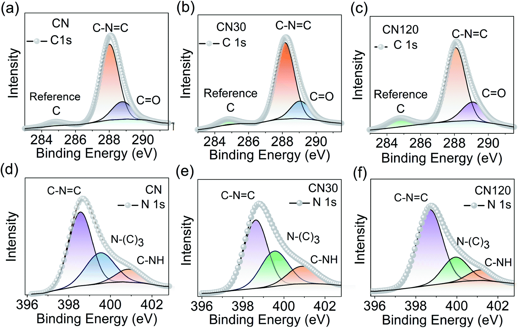
Another probing technique to quantify the surface composition is XPS. The XPS spectrum of CN, CN30, and CN120 is shown in Fig. 6. Fig. 6a–c shows the C 1s XPS spectrum from untreated and plasma-treated samples. After deconvolution, the C 1s peak of bulk CN generates three peaks at binding energies (B.E.) of 284.76 eV, 288.01 eV, and 288.76 eV. The results of the fitting are shown in Table S1.† The peak C1 at 284.76 eV is the reference carbon peak. The second peak (C2) at 288.01 eV comes from sp2 hybridized aromatic –C–NC bonding. The third peak (C3) at 288.76 eV is attributed to O–CO bonding. The deconvoluted N 1s spectra of bulk and plasma treated CN are shown in Fig. 6d–f. In bulk CN, the deconvoluted peak at 398.5 eV corresponds to sp2 hybridized two-coordinated nitrogen (N2C) in the C–NC bonding. The peak at 399.5 eV refers to sp3 hybridized three coordinated nitrogen (N3C) in N(C)3 bonding, and the 400.9 eV peak is due to C–NH bonding.32 The N(C)3 refers to either tertiary or bridging nitrogen atoms.23
 | ||
| Fig. 6 Surface compositional analysis using XPS. Deconvoluted C 1s and N 1s spectra of CN (a and d), CN30 (b and e), and CN120 (c and f). | ||
Fig. 7a shows the various C–N– bond cleavage processes as the plasma treatment time increases from 30 min to 120 min. Fig. 7b–d show the shifting in the C2 peak, N2C, and N3C peak as a function of plasma treatment time. In Fig. 7b, we see a shift in the C2 peak as time increases. After 30 min of treatment, the system is activated with intrinsic nitrogen-vacancy defects on the ring and on the bridging sites. The nitrogen-vacancy defects create positive charge on the carbon sites (Fig. 7a (1, 2)). Hence, the B.E. of the C2 peak in CN30 is shifted by 0.09 eV as compared to that of pure CN, as in Fig. 7b. In CN120, the shifting is 0.06 eV from that of pure CN. As time increases to 120 min, an excess amount of NO2− and NO3− binds with the unsaturated carbon atoms, shown in Fig. 7a (3).14,24 Therefore, it seems that the positive charge on carbon, developed due to the nitrogen-vacancy, is neutralized by the self-incorporated ions. But as the NO2− and NO3− groups in the system are more electronegative than carbon, they induce a positive charge on carbon, as shown in Fig. 7b. This results in a marginal blue shift in the B.E. peak in CN120. Fig. 7c and d show the B.E. shift of N2C and N3C peaks. As shown in Fig. 7c, the ring N2C peak in CN30 and CN120 undergoes 0.12 eV and 0.18 eV shifts to a higher B.E. as compared to pure CN. The unsaturated carbons, near the nitrogen-vacancy, bind with NO2− and NO3− groups forming –C–N–O– bonding, as shown in Fig. 7a (3, 4, 5). Further, the lone pair electrons on nitrogen are delocalized over the ring, leaving positive charges around nitrogen Fig. 7a (4, 5), and causing a blue-shift in the spectral position. Fig. 7d shows the shifting of the N3C peak. We can draw a similar conclusion for the blue shift in the B.E. peak for N3C, as we have provided for N2C. The self-incorporated groups are incorporated at the bridging site N3C position (Fig. 7a (6)) and bind with the carbon of the aromatic ring. Besides the –C–N–O– bonding, the rearrangement of bonding near the nitrogen-vacancy also generates –CN groups as added defects.
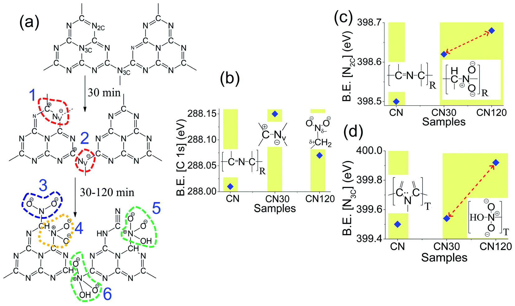 | ||
| Fig. 7 (a) Nitrogen vacancy formation with successive incorporation of NO2− and NO3− groups as self-incorporated defects into the framework of CN. Shifting in the B.E. position of the (b) C 1s peak, (c) N2C peak and (d) N3C peak corresponding to –C–NC– bonding for plasma-treated CN30 and CN120 samples in comparison to pure CN. The defects are incorporated on the ring (R) and the terminal (T) position. | ||
From XPS, we have also measured the N2C/N3C peak area ratio, and the results are incorporated in Table S1.† The ratio decreases from 1.94 in the bulk to 1.67 after 30 min of plasma treatment. A decrease in the N2C/N3C ratio indicates the generation of Nv on the N2C site. However, the N2C/N3C ratio again increases to 3.03 in CN120, which is even higher than that of bulk CN. A high N2C/N3C ratio is because of incorporation of NO2− and NO3− into the graphitic framework of CN. Thus, we have established defect evolution in CN nanosheets with PAS and XPS.
The synergy of plasma exfoliation and defect activation has an important implication on the samples' optical tunability. We can monitor the changes in the optical properties with UV-visible, steady-state photoluminescence (PL), and time-resolved photoluminescence (TRPL) spectroscopy.
Fig. 8a shows the absorption spectra of the samples. The spectra show a small hump at 330 nm corresponding to a π → π* transition, and a maximum at 370 nm for an n → π* transition.22 The n → π* transition involves photoexcitation from non-bonded (n) lone pair electrons on nitrogen near the valence band (VB) to the π* conduction band (CB). The n → π* transition is the free excitonic transition in CN.33–35 Besides the excitonic absorption, the plasma-treated samples show a broad visible absorption extending from 450–600 nm with a central maximum around 500 nm. The visible absorption is attributable to the presence of nitrogen-vacancies or self-incorporated defects. We see a colour variation in the plasma-treated samples because of these defects, as shown in Fig. 1b. The band gap variation with time is shown in Fig. 8b. The band gap increases until 90 min, then it starts to decrease, and at 150 min, the band gap attains a value nearly approaching that of bulk CN.
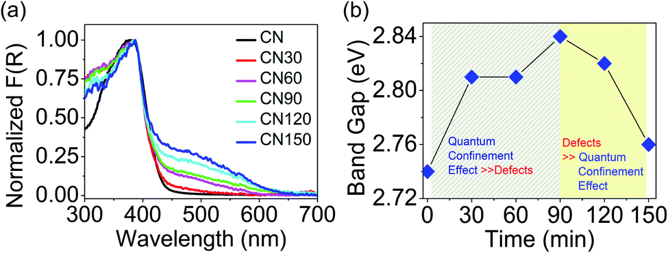 | ||
| Fig. 8 (a) Normalized absorption plot of the samples. (b) Band gap variation with plasma treatment. | ||
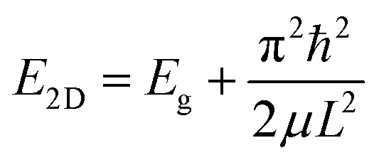
The increase in the band gap results from the quantum confinement (QC) effect in the exfoliated layers, and the decrease in the band gap occurs due to the intermediate defect states. As depicted in Fig. 8b, the contribution of quantum confinement and defects to the overall change in the band gap occurs concomitantly. We have presented a more elaborate discussion on the observed differences below. The relation between band gap enlargement with the layer thickness is explained with the following equation:
 | (1) |
Next, we have studied the emissive nature of the samples with steady-state photoluminescence (PL) and time-resolved PL spectroscopy. Fig. 9a and b show the room temperature PL spectra of the samples at 4.27 eV (π → π*), and 3.3 eV (n → π*) excitation.12 Both excitations result in a single broad emission spectrum with the central maximum around 2.8 eV. Although the spectral position remains unaltered, the emission intensity at 3.3 eV excitation is much stronger than at 4.27 eV. It is likely due to the abundance of carriers around the non-bonded N 2p states. Fig. 9c shows the PL and photoluminescence excitation (PLE) spectra of pure CN and CN150. The PLE spectra for the rest of the samples are shown in Fig. S1.† The maxima of PLE and PL are separated by 0.5 eV, as shown in Fig. 9c. The large energy difference indicates that the PL emission is not because of the free excitons, but due to the bound excitons. The bound excitons appear because of the association of the free exciton with vacancies and self-incorporated defects.
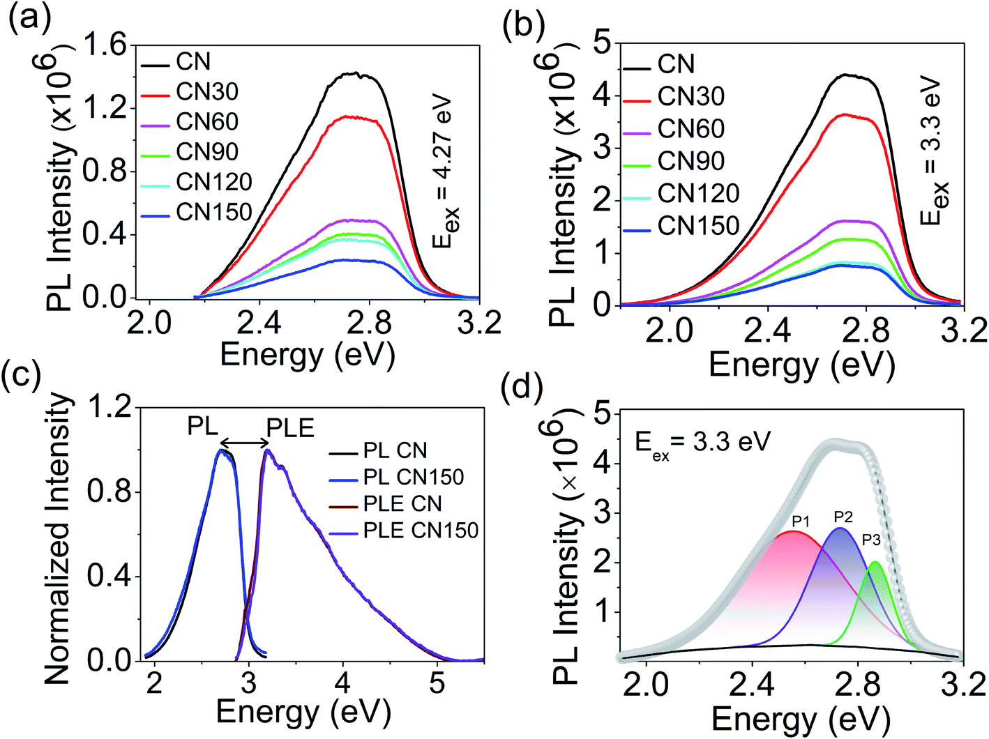 | ||
| Fig. 9 PL spectra of pristine and plasma-treated CN at excitation (a) 4.27 eV, and (b) 3.3 eV. (c) PL and PLE spectra of CN, and CN150 showing a difference of 0.5 eV. (d) PL spectra of CN fitted into three Gaussian peaks. | ||
We have further deconvoluted the broad PL emission into three Gaussians. The fitted peaks for bulk CN appear at 2.55 eV (P1), 2.73 eV (P2), and 2.86 eV (P3), as shown in Fig. 9d.
The fitted results for the plasma-treated samples are shown in Fig. S2.† We have plotted the maximum emission as a function of plasma treatment time. As the Fig. 10a shows, the P1 peak undergoes a red-shift by 0.1 eV after 150 min and, for the P2 peak, the spectral shift is 0.02 eV at 150 min. Plasma treatment has a negligible influence on the position of the P3 peak. It is seen that the spectral shift becomes more prominent as the energy separation between the free excitonic absorption (PLE) and emission (P1, P2, and P3) increases. The shift in P2 and P3 peaks is due to an increased number of bound excitonic states with the plasma treatment time. P1 peak emission appears far below the band gap of the samples. Unlike excitonic P2 and P3 emission, P1 emission can be associated with trapped state carriers. Because of the defect states acting as trap centres, we record a large spectral shift for the P1 trap state emission with the plasma exfoliation time.
Next, we see the impact of plasma exfoliation on the PL emission intensity and the broadening of the peak. In Fig. 9a and b we have noted a huge reduction in the emission intensity after plasma treatment, irrespective of the targeted excitation wavelength. By considering the fitted results with Gaussian, we have taken integrated PL intensity versus plasma exfoliation time. As shown in Fig. 10b, the emission intensity decays fast up to 60 min, and then decays slowly up to 150 min. The slow decay in emission intensity with time signifies a non-radiative excitonic emission because of high numbers in bound exciton density. An increase in exciton density facilitates exciton–exciton interactions which, as a result, increases the non-radiative emission decay. Further, an excess defect can dissociate the bound exciton into free carriers because of an elevated exciton-defect interaction. Once dissociated into free carriers, they are readily trapped at the defect states leading to a delay in recombination. In Fig. 10c, we have shown that the full width at half maximum (FWHM) of PL increases with the plasma discharging time. The increased PL band width with time implies an increased exciton–exciton interaction or increased interaction between trapped carriers.
 | ||
| Fig. 10 (a) Spectral shift of the PL maximum for deconvoluted P1, P2, and P3 peaks with plasma treatment time. Changes in the (b) integrated PL intensity and (b) full-width at half maximum (FWHM) of bulk and plasma-treated CN as a function of plasma exfoliation time. | ||
Time resolved PL spectroscopy measurements for the samples are conducted for a 2.78 eV emission at an excitation of 3.3 eV (Fig. 11). The PL decay is a tri-exponential temporal evolution under 3.3 eV photoexcitation, as shown in Table 2. The shortest component τ1 increases from 1.28 ns in bulk CN to 1.56 ns after 150 min of plasma treatment. Similarly, τ2 increases from 4.53 ns to 5.35 ns and τ3 increases from 20.4 ns to 22.9 ns in the bulk and 150 min of plasma treated samples, respectively.
 | ||
| Fig. 11 TRPL spectra of bulk and plasma-treated samples at an excitation of 3.3 eV and monitoring at 2.78 eV emission. | ||
| Sample | Lifetime (ns) | |||
|---|---|---|---|---|
| τ 1 (a1, %) | τ 2 (a2, %) | τ 3 (a3, %) | τ av | |
| CN | 1.28 (33.4) | 4.53 (51.2) | 20.4 (15.4) | 12.8 |
| CN30 | 1.38 (34.7) | 4.65 (49.4) | 21.5 (15.9) | 13.7 |
| CN60 | 1.41 (36.7) | 4.89 (49.3) | 22.0 (16.0) | 14.0 |
| CN90 | 1.40 (37.8) | 4.96 (46.1) | 22.4 (16.1) | 14.5 |
| CN120 | 1.47 (35.5) | 5.05 (47.6) | 22.7 (16.9) | 14.8 |
| CN150 | 1.56 (33.1) | 5.35 (47.4) | 22.9 (19.5) | 15.5 |
The average lifetime is extended from 12.8 ns in the bulk to 15.5 ns after 150 min of plasma-treatment. The origin of various PL lifetimes has been elaborately discussed in our earlier report.24 In a nutshell, the shortest lifetime is due to exciton movement and subsequent recombination in the stacked direction. The longest component of lifetime is due to the in-plane migration of excitons.15,38 The presence of nitrogen vacancies and self-incorporated nitrogenated species is likely to be responsible for the extended carrier lifetime.
In the introduction section, we have discussed that defects could be beneficial for an enhanced photocatalytic activity. However, there are some reports which are in favour of the above statement, and there are some reports which are against this statement. For example, Xue et al. showed that intermediate nitrogen vacancies and cyano defects in g-C3N4 enhance visible light absorption but reduce the mobility of electrons and holes. A reduced mobility restricts the overall improvement in photocatalytic activity.12 Similarly, Wu et al. remarked that –NH/NH2 terminals on g-C3N4 accelerate carrier recombination and limit the photocatalytic H2 evolution performance.39 In contrary to these reports, Li et al.,40 Zhang et al.,41 and Wen et al.18 showed that nitrogen vacancies and cyano defects enhance light absorption and facilitate carrier separation by trapping the carriers, resulting in improved methyl orange degradation, H2 production, and CO2 reduction. Niu et al.,42 however, stated that an improved photocatalytic performance requires an optimum defect concentration, beyond which the photocatalytic performance is greatly reduced.
To establish a correlation between photocatalytic activity and defects evolved in plasma modified CN, we performed photocatalytic removal of rhodamine B (RhB) from water under white LED illumination. The detailed experimental procedure is elaborated in the ESI.† The spectrum of the white LED is shown in Fig. S3.† The degradation of RhB is monitored by recording the decrease of the absorption maximum at 553 nm in the presence of CN and CN150 (Fig. 12a and b). The absorption spectra of degraded RhB with CN30 and CN90 are shown in Fig. S4.† The degradation is considered after subtracting the dye adsorption by the catalysts in the dark, which is shown in Fig. 12c. While bulk CN shows 75% removal of RhB, CN30 removes 89% of RhB under illumination. The photodegradation reduces to 88% in CN90 and 85% in CN150 (Fig. 12d). Therefore, though better photocatalytic activity of the plasma-treated samples is revealed compared to pristine CN under white light, our results directly complement the observation made by Xue et al.,12 and Niu et al.42 The increase in the photocatalytic activity in CN30 is likely due to the incorporated nitrogen vacancy defects in the system. These defects increase charge separation, making available sufficient carriers for involvement in photocatalysis. However, as the plasma exfoliation time increases, along with nitrogen vacancies, cyano defects, and self-incorporated defects also increase. From TRPL we have found that the average lifetime is much increased in CN150. Although the average lifetime is more, the mobility of charge carriers is expected to be lowered in the presence of excess defects, which finally lowers the efficiency of the photocatalysts in RhB degradation.
 | ||
| Fig. 12 Absorption spectra of RhB in the presence of (a) CN, and (b) CN150 showing gradual degradation of the central peak of RhB at 553 nm. (c) Adsorption of RhB on the catalyst surfaces during 45 minutes of stirring in the dark before illumination is shown as dark adsorption. (d) Degradation (in %) of RhB dye under white light in the presence of CN and plasma-treated CN. | ||
Finally, we have made a comparison (Table 3) of the advantages of our approach with other reported results for designing exfoliated and defect-activated g-C3N4 nanosheets towards photocatalytic applications.
| Method reported | Chemical/solvent used | Time duration | Report on exfoliation | Layer thickness achieved | Report on defect generation | Modification in absorption range | Photocatalytic performance | Reference |
|---|---|---|---|---|---|---|---|---|
| Chemical exfoliation | Sulphuric acid (98%) | 8 h | Yes | 0.4 nm | — | Blue shifted from 470 nm to 425 nm | Enhancement in photocatalytic activity | 9 |
| Chemical exfoliation | NMP and IPA | 10 h | Yes | 2 nm | — | Blue shifted from 2.35 eV to 2.65 eV | Enhanced photocatalytic H2 evolution | 11 |
| Liquid exfoliation | Water | 16 h | Yes | 2.5 nm | — | Blue shifted from 2.64 nm to 2.70 nm | Enhanced photoresponse and photocatalytic activity | 15 |
| Solvothermal exfoliation | IPA + H2O | 24 h | Yes | <0.5 nm | — | Blue shifted from 479 nm to 451 nm | Efficient H2 evolution | 43 |
| 12 h | 5 nm | |||||||
| Thermal polycondensation | DMF | 4 h calcination | Yes | 4 nm | — | Extended to 600 nm | Enhanced photocatalytic H2 production | 44 |
| Thermal treatment | — | 2–4 h | Yes | ∼1 nm | — | Blue shifted | Improved catalytic activity (desufurization) | 45 |
| Electrochemical method | NaOH | 40 min | Yes | 2 nm | — | — | Peroxidase like activity | 46 |
| Hydrothermal method | NaClO | 5 h | Yes | 4 nm | — | Red shifted from 2.75 eV to 2.55 eV | Enhanced photocatalytic activity, higher H2 evolution rate | 47 |
| Chemical (lithiation) | Liquid ammonia, lithium | ∼30 min | Yes | 2.5 nm | — | Blue shifted by 10 nm | Enhanced photocatalytic performance | 48 |
| Chemical (acidified) | H2SO4, HCl | ∼7 h (multistep process) | Yes | ∼1.5 nm | — | Blue shifted to 345 nm | Enhanced photocatalytic performance | 49 |
| Chemical | H2SO4 | 10 min (rapid) | Yes | <4 nm | — | Blue shifted to 443 nm | Enhance photocatalytic performance | 50 |
| Thermal polymerization | KOH | 4 h calcination (in situ) | — | Yes | Extended up to 500 nm | Limited enhancement in photocatalytic activity | 12 | |
| Thermal treatment | NH4Cl | 4 h calcination (in situ) | — | Yes | Red shifted to 2.65 eV | Enhanced photocatalytic H2 production rate | 17 | |
| Chemical | NaBH4 reduction | Up to 60 min | — | Yes | Extended up to 450 nm | 5-Fold increase in photocatalytic activity | 18 | |
| Thermal condensation | In presence of H2 gas | 4 h calcination, (in situ) | — | Yes | Extended up to 700 nm | Enhanced photocatalytic activity | 20 | |
| Thermal treatment | — | 4 h calcination+ 5 min thermal treatment | — | Yes | Extended up to 650 nm | Enhanced photocatalytic performance | 42 | |
| Air–liquid plasma exfoliation | Water | 150 min | Yes | Up to 3.78 nm | Yes | Extended up to 600 nm | Enhanced photodegradation of RhB under white light | Present report |
4. Conclusion
In summary, we have shown a novel approach of plasma-induced exfoliation of bulk g-C3N4. Without the aid of any chemicals and 150 min of plasma discharging, we achieve layer thinning to 3.78 nm. The peeling of the nanosheets' layers results from the electrostatic repulsion of intercalated NO2− and NO3− ions. The exfoliation is associated with the generation of nitrogen vacancies and self-incorporated nitrogen groups, as evident by PAS and XPS. The self-incorporated nitrogenated species form –CN and –C–N–O– bonds with the unsaturated carbons. The tunability of optical properties is linked with the reduced layer thickness and incorporated defects. The layer thickness is responsible for the enlargement of the band gap. However, nitrogen vacancies and self-incorporated defects are accountable for band gap reduction. The charge carrier dynamics reveal an increased carrier separation resulting from an increased exciton–exciton interaction. Since a reduced thickness and defects are considered requisites for designing an efficient photocatalytic system, we argue that this single step approach of plasma treatment is an efficient one to achieve defect activated CN nanosheets. The tested results for photocatalysis in RhB degradation under a white LED show an enhanced photocatalytic activity in the plasma-treated samples as compared to the untreated one. Defect states enhanced light absorption in the visible region and act as carrier trapping sites, resulting in the enhanced photocatalytic activity in CN30 (89%) as compared to pristine CN (75%). However, an increased exfoliation time reduces the photocatalytic activity in CN 90 (88%) and CN150 (85%). It is likely that excess defects reduce carrier mobility and degrade photo-induced catalytic activity in CN90 and CN150. The photocatalytic application of the synthesized material in water splitting under visible to NIR radiation is under progress in our laboratory.
Conflicts of interest
There are no conflicts of interest to declare.Acknowledgements
Biswajit Choudhury would like to acknowledge the Department of Science and Technology (Govt. of India) for supporting the research through the DST INSPIRE Faculty award. The authors also thank CSIR-NEIST, Jorhat for helping with the XPS facility.References
- X. Wang, K. Maeda, A. Thomas, K. Takanabe, G. Xin, J. M. Carlsson, K. Domen and M. Antonietti, Nat. Mater., 2009, 8, 76–79 CrossRef CAS PubMed.
- F. Dong, L. Wu, Y. Sun, M. Fu, Z. Wu and S. C. Lee, J. Mater. Chem., 2011, 21, 15171 RSC.
- F. Fina, S. K. Callear, G. M Carins and J. T. S. Irvine, Chem. Mater., 2015, 27, 2612–2618 CrossRef CAS.
- Z. Mao, J. Chen, Y. Yang, L. Bie, B. D. Fahlman and D. Wang, Carbon, 2017, 123, 651–659 CrossRef CAS.
- A. Kumar, P. Raizada, A. Hosseini-Bandegharaei, V. K. Thakur, V. H. Nguyen and P. Singh, J. Mater. Chem. A, 2021, 9, 111 RSC.
- J. S. Jang, H. G. Kim and J. S. Lee, Catal. Today, 2012, 185, 270–277 CrossRef CAS.
- T. Kashyap, S. Biswasi, A. R. Pal and B. Choudhury, ACS Sustainable Chem. Eng., 2019, 7, 19295–19302 CrossRef CAS.
- N. Rono, J. K. Kibet, B. S. Martincigh and V. O. Nyamori, Crit. Rev. Solid State Mater. Sci., 2020 DOI:10.1080/10408436.2019.1709414.
- J. Xu, L. Zhang, R. Shi and Y. Zhu, J. Mater. Chem. A, 2013, 1, 14766–14772 RSC.
- P. Niu, L. Zhang, G. Liu and H. M. Cheng, Adv. Funct. Mater., 2012, 22, 4763–4770 CrossRef CAS.
- S. Yang, Y. Gong, J. Zhang, L. Zhan, L. Ma, Z. Fang, R. Vajtai, X. Wang and P. M. Ajayan, Adv. Mater., 2013, 25, 2452–2456 CrossRef CAS PubMed.
- J. Xue, M. Fujitsuka and T. Majima, Phys. Chem. Chem. Phys., 2019, 21, 2318–2324 RSC.
- B. Choudhury and P. K. Giri, RSC Adv., 2016, 6, 24976–24984, 10.1039/c6ra00933f.
- F. Zhao, H. Cheng, Y. Hu, L. Song, Z. Zhang, L. Jiang and L. Qu, Sci. Rep., 2015, 4, 5882, DOI:10.1038/srep05882.
- X. Zhang, X. Xie, H. Wang, J. Zhang, B. Pan and Y. Xie, J. Am. Chem. Soc., 2013, 135, 18–21 CrossRef CAS PubMed.
- X. Sun, L. Shi, H. Huang, X. Song and T. Ma, Chem. Commun., 2020, 56, 11000 RSC.
- D. Zhang, Y. Guo and Z. Zhao, Appl. Catal., B, 2018, 226, 1–9 CrossRef CAS.
- Y. Wen, D. Qu, L. An, X. Gao, W. Jiang, D. Wu, D. Yang and Z. Sun, ACS Sustainable Chem. Eng., 2019, 7, 2343–2349 CrossRef CAS.
- V. w. Lau, I. Moudrakovski, T. Botari, S. Weinberger, M. B. Mesch, V. Duppel, J. Senker, V. Blum and B. V. Lotsch, Nat. Commun., 2016, 7, 12165 CrossRef CAS PubMed.
- Q. Tay, P. Kanhere, C. F. Ng, S. Chen, S. Chakraborty, A. Cheng, C. H. Huan, T. C. Sum, R. Ahuja and Z. Chen, Chem. Mater., 2015, 27(14), 4930–4933 CrossRef CAS.
- X. Bu, J. Li, S. Yang, J. Sun, Y. Deng, Y. Yang, G. Wang, Z. Peng, P. He, X. Wang, G. Ding, J. Yang and X. Xi, ACS Appl. Mater. Interfaces, 2016, 8, 31419–31425 CrossRef CAS PubMed.
- X. Ji, X. Yuan, J. Wu, L. Yu, H. Guo, H. Wang, H. Zhang, D. Yu and Y. Zhao, ACS Appl. Mater. Interfaces, 2017, 9, 24616–24624 CrossRef CAS PubMed.
- J. Aveyard, J. W. Bradley, K. McKay, F. McBride, D. Donaghy, R. Raval and R. A. D’Sa, J. Mater. Chem. B, 2017, 5, 2500–2510 RSC.
- B. Choudhury, K. K. Paul, D. Sanyal, A. Hazarika and P. K. Giri, J. Phys. Chem. C, 2018, 122, 9209–9219 CrossRef CAS.
- P. Heirman, W. V. Boxem and A. Bogaerts, Phys. Chem. Chem. Phys., 2019, 21, 12881–12894 RSC.
- H. D. B. Jenkins and K. P. Thakur, J. Chem. Educ., 1979, 56, 576 CrossRef CAS.
- W. G. Graham and K. R. Stalder, J. Phys. D: Appl. Phys., 2011, 44, 174037 CrossRef.
- Y. R. Luo, Handbook of Bond Dissociation Energies in Organic Compounds, CRC Press, Boca Raton, 1st edn, 2002 Search PubMed.
- H. Li, B. Zhu, S. Cao and J. Yu, Chem. Commun., 2020, 56, 5641–5644 RSC.
- D. Zhang, X. Han, T. Dong, X. Guo, C. Song and Z. Zhao, J. Catal., 2018, 366, 237–244 CrossRef CAS.
- D. Sanyal, T. K. Roy, M. Chakrabarti, S. De Choudhury, D. Bhowmick and A. Chakrabarti, J. Phys.: Condens. Matter, 2008, 20, 045217 CrossRef.
- J. R. Zhang, Y. Ma, S. Y. Wang, J. Ding, B. Gao, E. Kan and W. Hua, Phys. Chem. Chem. Phys., 2019, 21, 22819–22830 RSC.
- W. F. Espinosa-Garcia, J. M. Osorio-Guillen and C. M. Araujoc, RSC Adv., 2017, 7, 44997 RSC.
- C. Merschjann, T. Tyborski, S. Orthmann, F. Yang, K. Schwarzburg, M. Lublow, M. C. Lux-Steiner and T. S. Niedrig, Phys. Rev. B, 2013, 87, 205204 CrossRef.
- J. Bian, J. Li, S. Kalytchuk, Y. Wang, Q. Li, T. C Lau, T. A. Niehaus, A. L. Rogach and R. Q. Zhang, ChemPhysChem, 2015, 16, 954–959 CrossRef CAS PubMed.
- G. Y. Jia, Y. Liu, J. Y. Gong, D. Y. Lei, D. L. Wang and Z. X. Huang, J. Mater. Chem. C, 2016, 4, 8822–8828 RSC.
- S. Melissen, T. L. Bahers, S. N. Steinmann and P. Sautet, J. Phys. Chem. C, 2015, 119, 25188–25196 CrossRef CAS.
- C. Merschjann, S. Tschierlei, T. Tyborski, K. Kailasam, S. Orthmann, D. Hollmann, T. S. Niedrig, A. Thomas and S. Lochbrunner, Adv. Mater., 2015, 27, 7993–7999 CrossRef CAS PubMed.
- P. Wu, J. Wang, J. Zhao, L. Guo and F. E. Osterloh, J. Mater. Chem. A, 2014, 2, 20338–20344 RSC.
- K. Li, Y. Jiang, Y. Li, Z. Wang, X. Liu, P. Wang, D. Xia, R. Fan, K. Lin and Y. Yang, Int. J. Hydrogen Energy, 2020, 45, 9683–9694 CrossRef CAS.
- J. Zhang, J. Chen, Y. Wan, H. Liu, W. Chen, G. Wang and R. Wang, ACS Appl. Mater. Interfaces, 2020, 12, 13805–13812 CrossRef CAS PubMed.
- P. Niu, M. Qiao, Y. Li, L. Huang and T. Zhai, Nano Energy, 2018, 44, 73–81 CrossRef CAS.
- Q. Han, B. Wang, J. Gao, Z. Cheng, Y. Zhao, Z. Zhang and L. Qu, ACS Nano, 2016, 10, 2745–2751 CrossRef CAS PubMed.
- J. H. Zhang, M. J. Wei, Z. W. Wei, M. Pan and C. Y. Su, ACS Appl. Nano Mater., 2020, 3, 1010–1018 CrossRef CAS.
- G. Lei, Y. Cao, W. Zhao, Z. Dai, L. Shen, Y. Xiao and L. Jiang, ACS Sustainable Chem. Eng., 2019, 7, 4941–4950 CrossRef CAS.
- Q. Lu, J. Deng, Y. Hou, H. Wang, H. Li and Y. Zhang, Chem. Commun., 2015, 51, 12251 RSC.
- L. Cui, Y. Liu, X. Fang, C. Yin, S. Li, D. Sun and S. Kang, Green Chem., 2018, 20, 1354 RSC.
- Y. Yin, J. Han, X. Zhang, Y. Zhang, J. Zhou, D. Muir, R. Sutarto, Z. Zhang, S. Liu and B. Song, RSC Adv., 2014, 4, 32690 RSC.
- X. Du, G. Zou, Z. Wang and X. Wang, Nanoscale, 2015, 7, 8701–8706 RSC.
- L. R. Zou, G. F. Huang, D. F. Li, J. H. Liu, A. L. Pan and W. Q. Huang, RSC Adv., 2016, 6, 86688–86694 RSC.
Footnote |
| † Electronic supplementary information (ESI) available. See DOI: 10.1039/d1na00098e |
| This journal is © The Royal Society of Chemistry 2021 |