
 Open Access Article
 This Open Access Article is licensed under a Creative Commons Attribution-Non Commercial 3.0 Unported Licence
Inkjet printing of silver nanowires on flexible surfaces and methodologies to improve the conductivity and stability of the printed patterns†
Prathamesh
Patil‡
ab,
Suneha
Patil‡
a,
Prachi
Kate
a and
Amol A.
Kulkarni
 *a
*a
aChem. Eng. & Proc. Dev. Div., CSIR-National Chemical Laboratory, Pune, 411008, India. E-mail: aa.kulkarni@ncl.res.in
bChem. Eng. Dept., National Institute of Technology Calicut, Kozhikode, India
First published on 5th November 2020
Abstract
Silver nanowires (AgNWs) are known to be used for printing on rigid as well as flexible surfaces. Here we have developed a systematic approach for using AgNWs synthesized by the polyol method for printing on flexible surfaces using a simple inkjet printing method. Optimized ink formulation used in this work comprises a mixture of Ag NWs suspended in ethylene glycol directly taken after synthesis and isopropyl alcohol. Using such formulation saves time and loss of material while transferring to other solvents, which is the usual practice. The printed patterns demonstrate high conductivity and stability over many months, which can revolutionize the applications of functional nanomaterials in low-cost printed electronics. The importance of fragmentation of nanowires only to achieve specific aspect ratios, to facilitate easy jetting and to prevent clogging is demonstrated. Varied concentrations (10 mg mL−1 to 50 mg mL−1) of Ag NWs are used in ink formulations in order to print highly conductive patterns (resistance < 50 Ω sq−1) in a minimal number of passes. The same composition was also seen to facilitate simple and time-efficient nano-welding at room temperature, which improves the conductivity and stability of the printed patterns.
Introduction
The development of low cost printed electronic devices will be revolutionized by the ability to print conductive inks made of a wide range of functional nanomaterials in a simple and cost-efficient manner. Conductive ink formulations are typically made by diffusing conductive materials into a solvent and can conduct electricity after printing on an object, thus being a more economical approach to lay down modern conductive tracks. Due to applications in wide-ranging areas including solar photovoltaics,1 electronic textile and wearable electronics,1,2 3D printed electronics,3 flexible hybrid electronics (FHE), touch screen edge electrodes,4,5 automotive defoggers, seat occupancy sensors, seat heaters, etc., ITO replacement (hybrid, direct printing, etc.),6,7 electronic tattoos,8 touch screens for smart phones and tablets,5 fillers in high performance conductive adhesives9–11 and LEDs, LCDs and OLED displays,6,12 there is a huge booming consumer market for conducting inks. Furthermore, with the development of electronic printing technology, conductive thin films are widely used in flexible display circuit printing13 and to improvise or repair circuits on printed circuit boards as well. Conductive inks can be printed on flexible surfaces by several methods such as drop casting,14 spin coating,15,16 screen printing,17 digital printing (inkjet technology),3,13,18–23 gravure printing,24 flexography and the roller ball pen method.25 Among all the methods, inkjet has a high utilization of materials on a large area with precision and is a simple and low-cost manufacturing process.Inkjet printers are the most commonly used type of printers which recreate a digital image by propelling droplets of ink onto paper and plastic substrates. Depending on the utilization of the printing method, inks are often formulated with their distinctive stability and wettability. The composition of conductive ink comprises mainly a metal nanostructure in combination with solvents, capping agents, additives, antioxidants, UV absorbers and adhesion promoters. Functional nanomaterials such as gold nanoparticles, silver nanoparticles and nanowires, graphene, carbon nanotubes, copper nanoparticles, due to their enhanced thermal and electrical properties at the nanoscale and relatively very low quantity needed to achieve the desired performance attracted significant attention for their use in such applications.21 Amongst them, a one-dimensional form of silver, i.e. silver nanowires (AgNWs) has gained enormous demand because of its very high conductivity (6.30 × 10⁷ S m−1 at 20 °C; highest among all metals) and the high aspect ratio of nanowires helped enable their use in transparent conducting applications as well.21,26,27 Various methods have been developed for synthesizing Ag NWs such as the chemical reduction method,28 microwave-assisted synthesis,29 solvothermal method,30 template assisted method31 and ultra-violet irradiation method.32 The polyol method is one of the most reproducible methods27,33,34 used for the production of silver nanowires. The method involves using a polyol solvent such as ethylene glycol to reduce the precursor Ag+ ion to Ag0 to form single crystalline and mono-crystalline particles, which led to subsequent formation of nanowires by selective unidirectional growth. Synthesis of silver nanowires is a highly sensitive process as even a slight variation in the process parameters viz. temperature, concentrations (of the reducing agent, substrate an capping agent),the molecular weight of the capping agent, the reaction time, etc. can lead to a change in the diameter and aspect ratio (i.e. length) of nanowires and in turn affect their end-application.13 Silver nanowires with aspect ratios (<500) can be used in conductive ink compositions8,26,35 which can be printed on a wide range of rigid and flexible substrates to provide conductive thin films or coatings. External treatment methods such as sintering, laser and microwave techniques are carried out to further increase the conductivity in applications.36 Sintering is a heat treatment technique performed at room as well as high temperatures in order to improve the connection between two nanoparticles or nanowires.3,22,23,36,37 There is a need to improve the techniques for increasing the conductivity of the printed metallic networks. Thermal treatment requires precise control of the heating temperature and time as otherwise, the nanomaterial can oxidize or can get damaged on heat sensitive substrates especially plastics.38 Mechanical treatments such as pressing when applied to certain devices, high pressure may destroy some useful structures or the active layer. A simple but effective approach is using capillarity to improve the contact of wire junctions, which can form closely packed structures of nanoparticles that float or are immersed in liquids.39 In view of this we have studied the preparation of inkjet printing inks and developed a simple method to print highly conducting and stable patterns on flexible surfaces using the directly synthesized suspension of AgNWs in EG as it is.
The manuscript is organized as follows: after the Introduction, we have given details of experiments that involve developing formulations using silver nanowires. Further we have demonstrated the utilization of silver nanowires (in the form of conducting inks) for digital printing using easy-to-use inkjet printers. A detailed analysis of the number of passes and effective conductivity of the tracks on a paper is also presented. It was observed that our formulation was suitable for nano-welding at room temperature7 by applying moisture to the printed nanostructures, which helps increasing the number of points of contact. Furthermore, we have shown that by coating the surface of the nanowires with an additive polyaniline (PANI), not only the stability of the material is increased, but also a significant decrease in the resistance of the patterns is observed. Finally, we summarize the important findings.
Experimental
Materials
All chemical reagents were purchased from Merck GmbH and used without any further purification. Silver nitrate (AgNO3, 99.8%), Ethylene Glycol (EG, 99%), ferric chloride hexahydrate (anhydrous FeCl3·6H2O), and polyvinylpyrrolidone ((PVP) K90:360000) were used for the synthesis of silver nanowires. The synthesized silver nanowires (in ethylene glycol) were dispersed in isopropyl alcohol (99.7%) according to the optimal ink solvent ratio. For printing purposes, an A4 size paper sheet, PET sheet, commercial printer HP Deskjet Ink Advantage All-in-One Series – K209 were used.Synthesis procedure for AgNWs
Initially, ∼0.2 g of PVP was added to 22 mL of preheated Ethylene Glycol (EG) at 100 °C, and a constant stirring speed of 500 rpm, in a round bottom flask heated in an oil bath by means of an IKA C Mag HS7 digital heater. Then, 700 μM chloride solution (in EG) was added to the flask, which was then heated to a reaction temperature of 140 °C, after which AgNO3 solution (in EG) was added drop-wise to the reaction solution. The reaction was held at constant temperature for two hours and nanowire product solution of glistening silver-grey color was obtained, which was allowed to cool at room temperature. For purification of nanowires, product solution was precipitated using acetone (3 times the AgNW synthesis product) as an anti-solvent and the precipitate, after washing with ethanol was centrifuged at 13![[thin space (1/6-em)]](https://www.rsc.org/images/entities/char_2009.gif) 500 rpm for about one minute. The precipitate after centrifugation contained pure silver nanowires, which were further used in ink formulations.
500 rpm for about one minute. The precipitate after centrifugation contained pure silver nanowires, which were further used in ink formulations.
Preparation of AgNW ink
Pure silver nanowires were dispersed in a solution comprising a mixture of isopropyl alcohol and ethylene glycol. Ink samples were prepared on the basis of the weight of the nanowire per mL volume of solution of IPA:EG (85:15; volume%). The dispersion consisted of different concentrations of nanowire (10 mg mL−1, 20 mg mL−1, 30 mg mL−1, 40 mg mL−1 and 50 mg mL−1) samples with an average nanowire length of 10–13 μm. The prepared ink solutions (Fig. 1) were sonicated (to reduce the size of nanowires) for different intervals of time to optimize the length of nanowires so as to prevent clogging and allow unhindered passage of the sample through the nozzle of the cartridge.
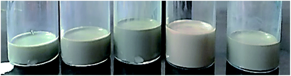 | ||
| Fig. 1 AgNW ink sample of IPA:EG in a ratio of 85:15 with the AgNW concentration ranging from 10 mg mL−1, 20 mg mL−1, 30 mg mL−1, 40 mg mL−1 to 50 mg mL−1 (left to right). | ||
Printing set up
Commercially available printer HP Deskjet Ink Advantage All-in-One Series – K209 was used for printing the nanowire suspensions. This printer has a HP Thermal Inkjet head with 336 nozzles and each nozzle is of size 10 μm (diameter), and each droplet volume is of the order of 2.5 picoliters. The printer consists of two cartridges, one in black and the other one in color. More details of the cartridge parameters are given in ESI Table 1.† The prints were taken on only single cartridge mode (black) (ESI Fig. 1† shows the image of the black cartridge used for printing). Parameters for the printing of silver nanowire ink such as print quality were set as ‘best’ and color options to ‘print in grey scale’ with ‘black ink only’. After making a few drawings, various prints of line patterns (length 10 cm and widths of 2, 4, 6, 8, 10 mm), squares, circles, helix and circuit patterns were taken on A4 sheets using the inkjet printer.Sintering and electrical measurements
Results and discussion
Optimization of the nanowire morphology by sonication
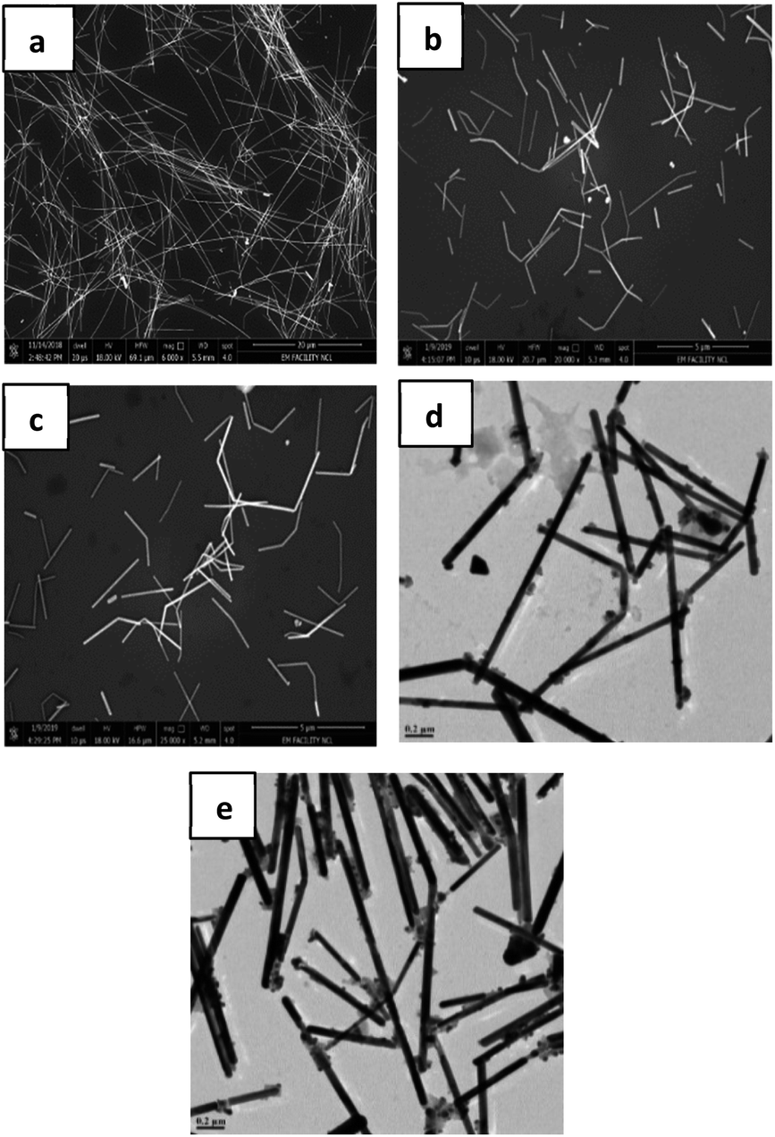 | ||
| Fig. 2 SEM images of AGNWs after sonication for (a) 0 min [50–100 μm], (b) 30 minutes [2–10 μm], and (c) 1 hour [1–5 μm]; TEM images of AgNWs after sonication for (d) 2 hours [0.8–1.8 μm], and (e) 3 hours [0.6–1.2 μm]. | ||
| Sonication time | Average length of the nanowire (μm) | Average diameter of the nanowire (nm) | Result |
|---|---|---|---|
| No sonication | 10–13 | 61 | Not jettable |
| 30 minutes | 3.77 | 61 | Cartridge gets clogged in the first print |
| 1 hour | 2.81 | 61 | Cartridge gets clogged after 5–6 prints |
| 2 hours | 1.72 | 61 | Optimum AgNW length for printing with no break in the conducting tracks |
| 3 hours | 1.18 | 61 | No clogging of the cartridge. Very short AgNWs result in lower conductivity when compared to sonication of 2 hours |
A comparison of the sonication effect on the length of two nanowire diameters (>100 nm and ∼60 nm) is plotted in Fig. 3a. Since, <2 μm (optimized length for NWs) is attained only for AgNWs with an average diameter of 60 nm or below, these NWs only can be considered for formulating conducting ink solutions for printing purpose.
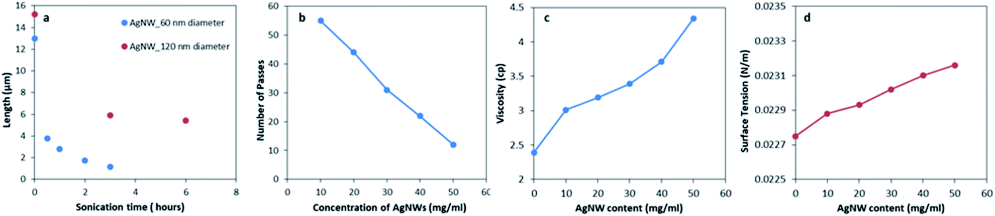 | ||
| Fig. 3 (a) Effect of the sonication time on fragmentation of silver nanowires; (b) number of printing passes required with respect to the concentration of AgNWs; (c) and (d) viscosity and surface tension variation of the ink sample respectively with respect to the concentration of AgNWs in the ink sample. | ||
Optimization of the concentration of nanowires in ink
According to most of the literature, 10–15 numbers of passes are an acceptable range of repeated passes to make a pattern conductive. However, in general, it is necessary to minimize the number of passes and yet obtain a conducting track. Here we have obtained optimal numbers of passes by increasing the concentration of the nanowire concentration in the ink from 10 to 50 mg mL−1. With increase in the AgNW concentration, the numbers of passes required to make the pattern conductive decreased, which is plotted in Fig. 3b. For 50 mg mL−1 concentration, the numbers of passes to obtain a continuous conducting track was 12, which agrees with the literature data.The two most important properties of ink are viscosity (resistance to flow) and surface tension as they decide the ease of detachment from the nozzle and also spreading on the surface. The viscosity and surface tension of the samples were measured and are shown in Fig. 3c and d respectively. The values of both viscosity and surface tension were seen to increase with the silver concentration and are in agreement with data in the literature.18 For the weight concentration of mere 5% silver nanowires (50 mg mL−1), the ink sample has a viscosity of ∼4.4 cP, which is in the acceptable range of commercial inkjet printing inks (1–30 cP).18,20 The relatively lower surface tension (∼23 mN m−1 when compared to 27–35 mN m−1 in commercially available ink18) can be increased by increasing the wt% of Ag in the sample. However, in our case, using 5 wt% concentration does not affect printing significantly because after the addition of the additive the surface tension of the sample measures in the permissible range (∼30 mN m−1). Utilization of silver nanowires in inkjet inks is beneficial because these nanowire-based inks perform well in printing even at very low concentrations of silver (5 wt%) as compared to commercially available AgNP based inks with much higher Ag concentrations (19–21%).22,23 Inkjet printing is more appropriate for AgNW inks as the method works well for such low viscosity inks.
Stability of nanowires
Additives are key factors in the production of high-performance conductive inks, and also should be compatible with the nano materials and substrates used. Polyaniline (PANI), polythiophene, and polypyrrole (PPy) can be used as stabilizing agents as they are conductive polymers, but among all conductive polymers PANI has the highest conductivity because of the C–N extended conjugation while all other polymers have a C–C single bond. PANI was chosen as the stabilizing agent due its higher conductivity and stronger antioxidant properties in this work. Chemical synthesis of PANI requires three reactants aniline, an acidic medium and an oxidant. Hydrochloric acid (HCl) and sulphuric acid (H2SO4) are the most common acids used for synthesis. As for oxidants, it is recommended to use ammonium persulfate ((NH4)2S2O8), potassium dichromate (K2Cr2O7), cerium sulphate (Ce(SO4)2), sodium vanadate (NaVO3), potassium ferricyanide (K3(Fe(CN)6)), potassium iodate (KIO3), and hydrogen peroxide (H2O2).11 We have used the most common chemical oxidation method in which the oxidant to aniline ratio is kept as 1:1 in order to obtain high conductivity. Synthesis is performed by mixing 0.29 mol L−1 aqueous HCl solution with a mixture of 0.28 mol L−1 aniline and 0.28 mol L−1 ammonium persulfate and stirred at 2 rpm.37 The reaction temperature was maintained at 0–2 °C for 2 hours. The precipitate obtained was removed by filtration and washed with HCl and vacuum-dried for 1 hour. The prepared PANI powder was then added to the ink sample in various weight percentages such as 1%, 3% and 5% of the weight of the AgNWs in ink formulation. The above figures represent the FTIR spectra of polyaniline and polyaniline–silver nanowire composite ink. Fig. 4a presents the FTIR spectra of PANI in which characteristic peaks of PANI were observed at 757 cm−1 (m-disubstituted Ar C–H bend), 1688 cm−1 (C![[double bond, length as m-dash]](https://www.rsc.org/images/entities/char_e001.gif) C, leucoemeraldine), 1250 cm−1 (C–N stretching vibrations, CAr–N) and 3333 cm−1 (N–H stretching). The strong peaks at 2891 cm−1 are assigned to the asymmetric and symmetric stretching vibration modes of methyl groups.40 The characteristic absorption bands at 1037 cm−1 correspond to the (CN) stretching vibration,41 whereas the sharp peak at 1457 cm−1 corresponds to the stretching mode of the N–B–N group of protonated PANI.42 The peak at 3834 cm−1 is because of the N–H stretching vibration of the amino group of polyaniline.43
C, leucoemeraldine), 1250 cm−1 (C–N stretching vibrations, CAr–N) and 3333 cm−1 (N–H stretching). The strong peaks at 2891 cm−1 are assigned to the asymmetric and symmetric stretching vibration modes of methyl groups.40 The characteristic absorption bands at 1037 cm−1 correspond to the (CN) stretching vibration,41 whereas the sharp peak at 1457 cm−1 corresponds to the stretching mode of the N–B–N group of protonated PANI.42 The peak at 3834 cm−1 is because of the N–H stretching vibration of the amino group of polyaniline.43
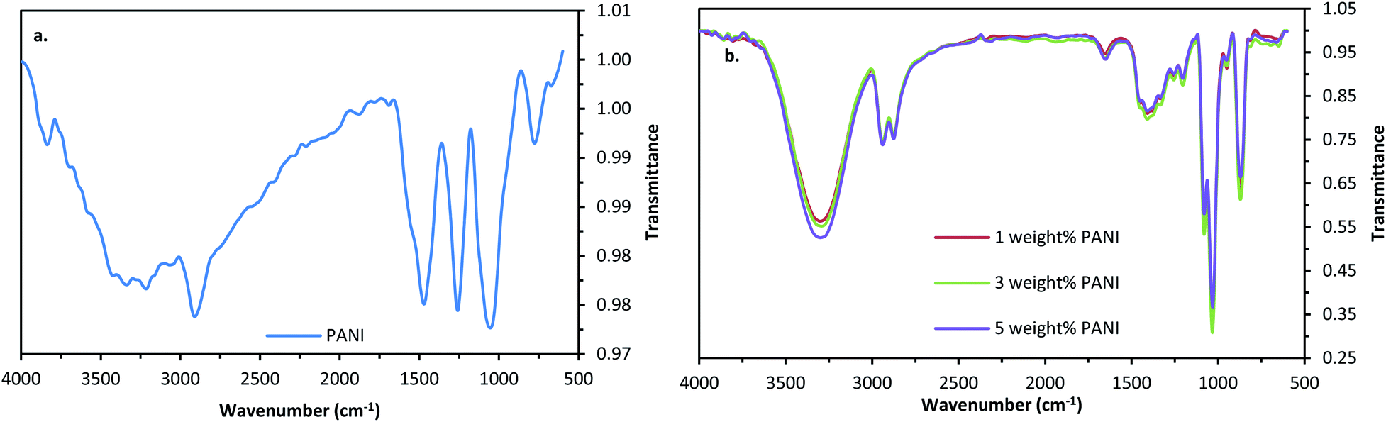 | ||
| Fig. 4 Infrared spectra of (a) PANI; (b) 1 wt%, 3 wt% and 5 wt% PANI–AgNW conductive ink. | ||
Fig. 4b presents the FTIR spectra of the 1 wt%, 3 wt% and 5 wt% PANI–AgNW conductive ink respectively. It is observed that, even though the wt% of PANI in the ink formulation is changed from 1 wt% to 5 wt%, the FTIR spectra remain unchanged. The majority of the above listed characteristic PANI peaks could be observed in the PANI/Ag spectrum with some overlapping and intensity changes (Fig. 4b). From the comparison between PANI FTIR spectra and the rest all FTIR spectra, it can be seen that 3333 cm−1 (N–H stretching) and 2891 cm−1 (C–H stretching) appear as sharp peaks, and 757 cm−1 (m-disubstituted Ar C–H bend) has shifted to 863 cm−1. On the other hand 1250 cm−1 (C–N stretching vibrations, CAr–N), and 1037 cm−1 (CN stretching vibration) were shifted to 1050 cm−1 and 1028 cm−1 respectively. This could happen due to a change in the stretching frequency (which only depends on the force and reduced mass) and can be obtained as γ = 1/(2πC)√(k/μ), where γ is the stretching frequency, C is the speed of light, k is the force constant, and μ = reduced mass. During doping of silver nanowires with PANI, the reduced mass remains unchanged and the stretching frequency could vary depending on the force constant. A change in charge transfer leads to a change in the force constant. Thus, the AgNW surface gets coated by PANI through the interaction between silver and the C–N bond of PANI.
The prepared sample was spin coated on the glass substrate which shows a far-reaching difference in the conductivity of the coated sample. The sample without the PANI content showed a resistance of about 584 Ω □−1, when coated on a glass substrate at 1000 rpm for 60 s. On the other hand under the same spin coating conditions, ink samples with 1 wt%, 3 wt% and 5 wt% PANI content show low average resistances of 62 Ω □−1, 55 Ω □−1 and 47.5 Ω □−1 respectively. It was observed that resistance reduced by ∼90% of its initial value after the addition of PANI, and the resistance remains more or less the same, irrespective of the PANI weight percentage. This implies that even a small quantity (1 wt% PANI or lower) is enough to coat the whole surface of silver nanowires to reduce the average resistance to <60 Ω □−1.
Sintering of nanowires
In order to achieve a highly conductive pattern, sintering of printed nanowires is required. The most common technique for sintering the nanowires is by conventional heating in an oven or on a hot plate, which requires high temperature as well as long sintering times.23 Also, there is a possibility of some temperature sensitive substrates getting deformed at high temperatures, thereby leading to oxidation of nanowires in short periods of time. The sintering process usually consists of 2 stages. In the first stage, thermal decomposition and removing of the surfactant (capping agent) are the dominating phenomena. In this stage the high resistance of the printing structure remains stable, because nanowires are separated by organic layers and do not touch each other. In the second stage, the protective layer is removed so that nanoparticles would form at the metallic contact and hence, the diffusion and recrystallization phenomena play the dominating role.22 At the beginning of the second stage, resistance drops significantly due to formation of many chemical paths between the nanoparticles. In this work, we have opted for another sintering method also known as the moisture treatment method. Here, the coated sample was subjected to water vapour for 1 minute, so that vapour condenses and gets trapped at the contact of the nanowires and due to the capillary force action, the nanowires on the top bend at the contact point after drying.8Effect of sintering on electrical measurements
The images of AgNW spin coated samples for the surface morphology after undergoing heat treatment at different temperatures for 60 min each are shown in Fig. 5b. A visible effect of sintering on the AgNW samples is seen from the images at temperatures > 175 °C, which instigates the increase in contact between the nanowires and is further confirmed by a decrease in electrical resistance at higher temperatures which is plotted in Fig. 5a as a function of temperature and time. At higher temperatures, the nanowires start melting into nanoparticles, which was due to the evaporation of solvents, thus increasing the interaction between the nanowires and resulting in a significant drop in the resistance. Very high resistances initially are a result of fragmented nanowires. A sudden drop in resistance was observed with the first 10 minutes of heat treatment for the temperature range of 175–300 °C. The resistance continued to drop steadily until 1 hour. In case of lower temperatures such as 140 °C; the resistance of the sample was 403 Ω sq−1 by the end of 1 hour of heat treatment (a drop by ∼725% in the initial value of 2900 Ω sq−1), whereas, for higher temperatures such as above 300 °C, there was a substantial drop in the initial readings to reach as low as ∼3 Ω sq−1 by 1 hour. It is clear from Fig. 6 that very low resistances (<15 Ω sq−1) could be achieved only by treating the samples at temperatures above 200 °C. Moreover, the conductivity of the sample could be influenced by altering the temperature and time of heat treatment. For example, one could obtain highly conductive samples (∼6 Ω sq−1 resistance) within 35 minutes of treatment by either increasing the temperature above 225 °C or by keeping lower temperatures at the expense of prolonged treatment times of 60 minutes (∼15 Ω sq−1 at 210 °C). But in view of the time required to reach lower values, it was felt that heating the sample at 300 °C for only 10 min would still be a better choice.
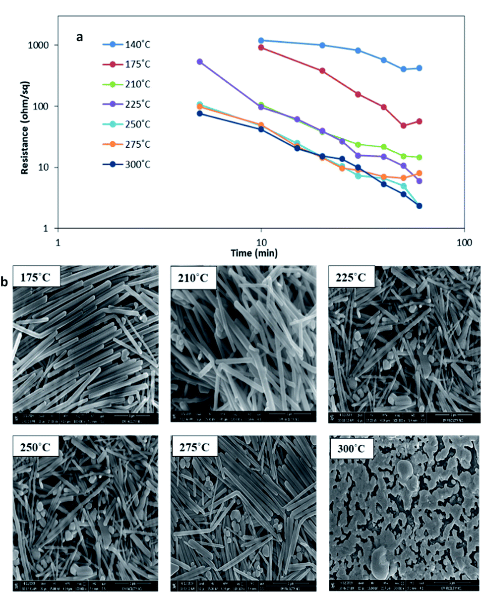 | ||
| Fig. 5 (a) Electrical resistance as a function of temperature and time and (b) SEM images of silver nanowires after thermal sintering treatment at different temperatures. | ||
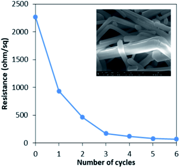 | ||
| Fig. 6 Electrical resistance after moisture treatment and the inset image showing the NW morphology after moisture treatment. | ||
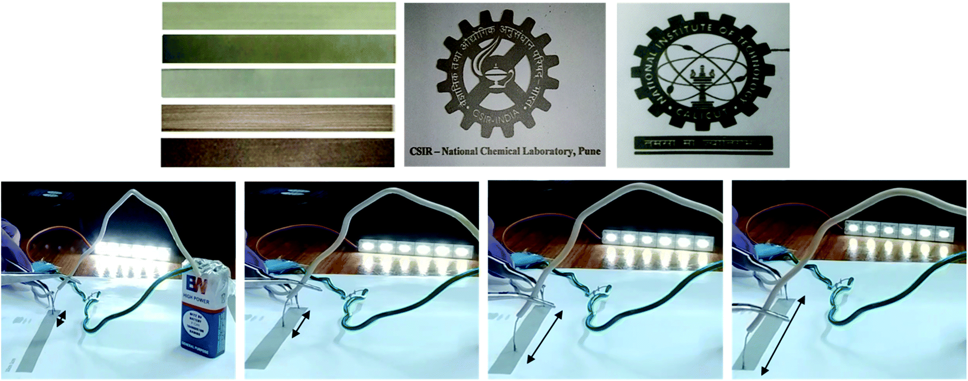 | ||
| Fig. 7 (Top row) (left) Conductive patterns of AgNW lines at different concentrations (10 mg mL−1, 20 mg mL−1, 30 mg mL−1, 40 mg mL−1, and 50 mg mL−1 from top to bottom) and (middle and right) logos of CSIR and NITC printed on an A4 sheet of printing paper; (bottom row) verification of conducting tracks for lighting of LEDs and the effect of the distance between the contact points on the intensity. | ||
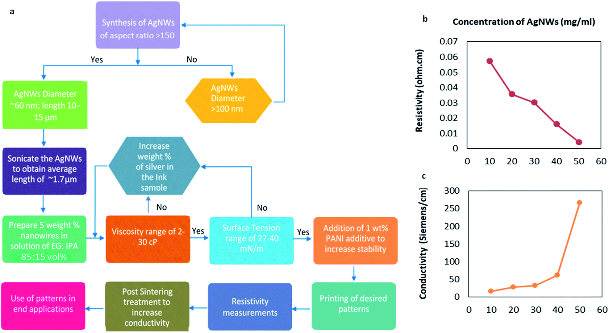 | ||
| Fig. 8 (a) Flowchart representing the procedure for printing of silver nanowire conducting inks and the effect of the AgNW concentration on (b) resistivity and (c) conductivity. | ||
Conclusions
Printing of conducting tracks on regular A4 size paper using a commercially available inkjet printer having silver nanowire ink is demonstrated with a highly reproducible protocol. Continuous and smooth lines of a conducting pattern are achieved in 12 passes and the tracks are conductive even after several months after printing. Printing was achieved using nanowires of 1.72 μm length and a diameter of ∼60 nm. The nanowires are synthesized by chemical reduction with polyol and dispersed in a simple co-solvent system made of ethylene glycol and isopropyl alcohol to get a conductive ink with a mere 5 wt% concentration of Ag. Importantly, unlike most of the literature that involves transfer of conducting nanowires into other solvents, here we have used AgNWs synthesized directly in EG as it is to make ink formulations. This approach has helped us ensure no loss of this exotic material without compromising on the quality of conducting patterns or their printability. A systematic and reproducible work flow was evolved for making Ag NW inks that can be used for printing conducting tracks. A wire diameter <70 nm and very short lengths corresponding to ∼1.8 μm avoid clogging of the cartridge nozzles and ensure a smooth printing process. Nanowire segments of smaller lengths can flow through the nozzles but need significantly higher loading.Many literature reports mention the use of silver nanoparticle inks with a higher Ag concentration ranging from 15–40 wt%.13,44–46 Although commercially available inks require only one pass, using a higher amount of silver will be significantly expensive, since the cost of nano-silver itself will outweigh the cost of the whole printing operation. Using AgNW ink is practical because it is economically feasible to give a greater number of passes (12 in our case) compared to increasing the nano-silver concentration in the ink. It also needs to be realized that the sintering of nanoparticles or nanowires is essential during their printing. Using nanoparticles indeed needs a high loading to avoid breaks in the printed paths, which can be avoided by using a low loading of silver nanowires. Inks made using silver nanowires require a very low concentration of AgNWs and perform very well, thus proving their commercial use in many electronic applications.
The stability of AgNW inks as well as the overall conductivity can be increased by addition of very small quantities of additives such as polyaniline PANI (1%). A post-treatment of sintering of the conductive patterns reduces the resistance (<100 Ω) and sintering carried out on a spin coated sample (300 °C for 10 min) showed a very low electrical resistance of 2.63 × 10⁻⁴ Ω cm after 60 minutes of continuing the treatment (from initial value of 4.7 × 10⁻³ Ω cm). An alternate to the heat treatment, capillary force induced nano-welding at room temperature is found to improve the conductivity without applying heat, which was carried out by giving moisture treatment, and can be the best treatment for heat sensitive substrates. The resistance of samples reduced from 465 Ω sq−1 (in the first two cycles) to as low as 71 Ω sq−1 (resistivity of 8.023 × 10⁻³ Ω cm) after 6 times of moisture treatment.
Conflicts of interest
There are no conflicts to declare.Acknowledgements
The authors acknowledge the funding from DST (GoI) Advanced Manufacturing Technologies Scheme. Prathamesh Patil thanks the Chemical Engineering Department of NIT Kozhikode for allowing him to do his MTech project at NCL.Notes and references
- N. Espinosa, R. R. Søndergaard, M. Jørgensen and F. C. Krebs, ChemSusChem, 2016, 9, 893–899 CrossRef CAS.
- S. J. Choi, S. J. Kim, J. S. Jang, J. H. Lee and I. D. Kim, Small, 2016, 12, 5826–5835 CrossRef CAS.
- J. Vaithilingam, M. Simonelli, E. Saleh, N. Senin, R. D. Wildman, R. J. M. Hague, R. K. Leach and C. J. Tuck, ACS Appl. Mater. Interfaces, 2017, 9, 6560–6570 CrossRef CAS.
- D. Bellet, M. Lagrange, T. Sannicolo, S. Aghazadehchors, V. H. Nguyen, D. P. Langley, D. Muñoz-Rojas, C. Jiménez, Y. Bréchet and N. D. Nguyen, Materials, 2017, 10(6), 1–16 CrossRef.
- C. Mayousse, C. Celle, E. Moreau, J. F. Mainguet, A. Carella and J. P. Simonato, Nanotechnology, 2013, 24(21), 215501 CrossRef.
- H. Lee, M. Kim, I. Kim and H. Lee, Adv. Mater., 2016, 28, 4541–4548 CrossRef CAS.
- Y. Liu, J. Zhang, H. Gao, Y. Wang, Q. Liu, S. Huang, C. F. Guo and Z. Ren, Nano Lett., 2017, 17, 1090–1096 CrossRef CAS.
- N. X. Williams, S. Noyce, J. A. Cardenas, M. Catenacci, B. J. Wiley and A. D. Franklin, Nanoscale, 2019, 11, 14294–14302 RSC.
- P. Zhang, I. Wyman, J. Hu, S. Lin, Z. Zhong, Y. Tu, Z. Huang and Y. Wei, Mater. Sci. Eng., B, 2017, 223, 1–23 CrossRef CAS.
- Y. Liu, X. Yang, L. Yue, W. Li, W. Gan and K. Chen, Polym. Compos., 2019, 40, 4390–4401 CrossRef CAS.
- Y. Sun, Nanoscale, 2010, 2, 1626–1642 RSC.
- J. Kwon, Y. D. Suh, J. Lee, P. Lee, S. Han, S. Hong, J. Yeo, H. Lee and S. H. Ko, J. Mater. Chem. C, 2018, 6, 7445–7461 RSC.
- L. Cao, X. Bai, Z. Lin, P. Zhang, S. Deng, X. Du and W. Li, Materials, 2017, 10(9), 1–9 CrossRef CAS.
- S.-H. Tseng, L.-M. Lyu, K.-Y. Hsiao, W.-H. Ho and M.-Y. Lu, Chem. Commun., 2020, 56(42), 5569–5706 RSC.
- J. Sun, W. Zhou, H. Yang, X. Zhen, L. Ma, D. Williams, X. Sun and M. F. Lang, Chem. Commun., 2018, 54, 4923–4926 RSC.
- S. Fahad, H. Yu, L. Wang, A. Nazir, R. S. Ullah, K. ur R. Naveed, T. Elshaarani, B. U. Amin, A. Khan and S. Mehmood, J. Mater. Sci.: Mater. Electron., 2019, 30, 12876–12887 CrossRef CAS.
- W. R. De Araujo and W. R. Paixão, Analyst, 2014, 139, 2742–2747 RSC.
- H. H. Lee, K. Sen Chou and K. C. Huang, Nanotechnology, 2005, 16, 2436–2441 CrossRef CAS.
- N. C. Raut and K. Al-Shamery, J. Mater. Chem. C, 2018, 6, 1618–1641 RSC.
- Z. Liu, Y. Su and K. Varahramyan, Thin Solid Films, 2005, 478, 275–279 CrossRef CAS.
- D. J. Finn, M. Lotya and J. N. Coleman, ACS Appl. Mater. Interfaces, 2015, 7, 9254–9261 CrossRef CAS.
- W. Zhou, F. A. List, C. E. Duty and S. S. Babu, Metall. Mater. Trans. B, 2015, 46, 1542–1547 CrossRef CAS.
- D. Tobjörk, H. Aarnio, P. Pulkkinen, R. Bollström, A. Määttänen, P. Ihalainen, T. Mäkelä, J. Peltonen, M. Toivakka, H. Tenhu and R. Österbacka, Thin Solid Films, 2012, 520, 2949–2955 CrossRef.
- E. Hrehorova, M. Rebros, A. Pekarovicova, B. Bazuin, A. Ranganathan, S. Garner, G. Merz, J. Tosch and R. Boudreau, IEEE/OSA J. Disp. Technol., 2011, 7, 318–324 Search PubMed.
- A. Russo, B. Y. Ahn, J. J. Adams, E. B. Duoss, J. T. Bernhard and J. A. Lewis, Adv. Mater., 2011, 23, 3426–3430 CrossRef CAS.
- R. Z. Li, A. Hu, T. Zhang and K. D. Oakes, ACS Appl. Mater. Interfaces, 2014, 6, 21721–21729 CrossRef CAS.
- N. M. Abbasi, H. Yu, L. Wang, Z. Abdin, W. A. Amer, M. Akram, H. Khalid, Y. Chen, M. Saleem, R. Sun and J. Shan, Mater. Chem. Phys., 2015, 166, 1–15 CrossRef CAS.
- Y. Sun, Y. Yin, B. T. Mayers, T. Herricks and Y. Xia, Chem. Mater., 2002, 14, 4736–4745 CrossRef CAS.
- M. Tsuji, Y. Nishizawa, K. Matsumoto, M. Kubokawa, N. Miyamae and T. Tsuji, Mater. Lett., 2006, 60, 834–838 CrossRef CAS.
- Y. Li, S. Guo, H. Yang, Y. Chao, S. Jiang and C. Wang, RSC Adv., 2018, 8, 8057–8063 RSC.
- X. Jiang, Y. Xie, J. Lu, L. Zhu, W. He and Y. Qian, J. Mater. Chem., 2001, 11, 1775–1777 RSC.
- Y. Zhou, S. H. Yu, C. Y. Wang, X. G. Li, Y. R. Zhu and Z. Y. Chen, Adv. Mater., 1999, 11, 850–852 CrossRef CAS.
- S. Coskun, B. Aksoy and H. E. Unalan, Cryst. Growth Des., 2011, 11, 4963–4969 CrossRef CAS.
- A. Nekahi, S. P. H. Marashi and D. H. Fatmesari, Mater. Chem. Phys., 2016, 184, 130–137 CrossRef CAS.
- X. Yang, D. Du, Y. Wang and Y. Zhao, Micromachines, 2018, 10, 1–10 CrossRef.
- M. Hummelgård, R. Zhang, H. E. Nilsson and H. Olin, PLoS One, 2011, 6, 1–6 CrossRef.
- Z. Wang, W. Wang, Z. Jiang and D. Yu, Prog. Org. Coat., 2016, 101, 604–611 CrossRef CAS.
- A. Kamyshny and S. Magdassi, Small, 2014, 10, 3515–3535 CrossRef CAS.
- Y. Hu, Z. Lao, B. P. Cumming, D. Wu, J. Li, H. Liang, J. Chu, W. Huang and M. Gu, Proc. Natl. Acad. Sci. U. S. A., 2015, 112, 1–6 CrossRef.
- C. Dispenza, M. A. Sabatino, D. Chmielewska, C. Lopresti and G. Battaglia, React. Funct. Polym., 2012, 72(3), 185–197 CrossRef CAS.
- Z. A. Hu, Y. L. Xie, Y. X. Wang, L. P. Mo, Y. Y. Yang and Z. Y. Zhang, Mater. Chem. Phys., 2009, 114(2–3), 990–995 CrossRef CAS.
- S. Poyraz, I. Cerkez, T. S. Huang, Z. Liu, L. Kang, J. Luo and X. Zhang, ACS Appl. Mater. Interfaces, 2014, 6(22), 20025–20034 CrossRef CAS.
- J. Coates, Interpretation of Infrared Spectra, A Practical Approach, in Encyclopedia of Analytical Chemistry, ed. R. A. Meyers, John Wiley & Sons Ltd, Chichester, UK, 2000, pp. 10815–10837 Search PubMed.
- M. Arunakumari, A. G. Mayes and M. S. Alexander, Materials, 2019, 1–10 Search PubMed.
- E. Balliu, H. Andersson, M. Engholm, T. Öhlund, H. E. Nilsson and H. Olin, Sci. Rep., 2018, 8, 2–10 CrossRef.
- I. J. Fernandes, A. F. Aroche, A. Schuck, P. Lamberty, C. R. Peter, W. Hasenkamp and T. L. A. C. Rocha, Sci. Rep., 2020, 10, 1–11 CrossRef.
Footnotes |
| † Electronic supplementary information (ESI) available. See DOI: 10.1039/d0na00684j |
| ‡ Equal contribution. |
| This journal is © The Royal Society of Chemistry 2021 |