
 Open Access Article
 This Open Access Article is licensed under a Creative Commons Attribution-Non Commercial 3.0 Unported Licence
Thermal conductivity measurements of thin films by non-contact scanning thermal microscopy under ambient conditions†
Yun
Zhang
,
Wenkai
Zhu
and
Theodorian
Borca-Tasciuc
 *
*
Mechanical, Aerospace, and Nuclear Engineering Department, Rensselaer Polytechnic Institute, Troy, NY 12180, USA. E-mail: borcat@rpi.edu
First published on 14th December 2020
Abstract
Thermal conductivity measurements using Scanning Thermal Microscopy (SThM) usually involve heat transfer across the mechanical contact and liquid meniscus between the thermal probe and the sample. However, variations in contact conditions due to capillary effects at probe–sample contact and probe and sample wear due to mechanical contact interfere with accurate determination of the thermal conductivity. This paper presents measurements of thin film thermal conductivity using a SThM method employing a Wollaston probe in non-contact mode in synergy with detailed heat transfer analysis. In this technique, the thermal probe is scanned above the sample at a distance comparable with the mean free path of the ambient gas molecules. A Three-Dimensional Finite Element Model (3DFEM) that includes the specifics of the heat transfer between the sample and the probe in transition heat conduction regime was developed to predict the SThM probe thermal resistance and fit the thermal conductivity of the measured thin films. Proof-of-concept experimental in-plane thermal conductivity results for 240 nm and 46.6 nm Au films deposited on glass and silicon substrates were validated by experimental measurements of their electrical conductivity coupled with the Wiedemann–Franz law, with a discrepancy < 6.4%. Moreover, predictions based on a kinetic theory model for thin-film thermal conductivity agreed with the experimental results for the Au films with <6.6% discrepancy. To reduce the time and complexity of data analysis and facilitate experimental planning, an analytical model was also developed for the thermal transport between the Wollaston probe, ambient, and film-on-substrate samples. The accuracy of thin film thermal conductivity measurements using the analytical model was investigated using 3DFEM simulations. Fitted functions were developed for fast data analysis of thermal conductivity of thin films in the range of ∼100–600 W m−1 K−1 and thickness between ∼50–300 nm deposited on the two types of substrates investigated in this work, which yielded results with a discrepancy of 6–16.7% when compared to the Au films' thermal conductivity values.
1. Introduction
The ability to accurately and versatilely determine the thermal conductivity (kf) for thin films is critical for the performance and thermal management of devices based on these low-dimensional materials.1 However, measuring high thermal conductivity materials at the nanoscale is a challenging task.2–4 Over the last two decades various techniques had been developed to characterize the thermal conductivity with improving adaptability and spatial resolution. Among them Scanning Thermal Microscopy (SThM) based techniques employ thermal probes with superior spatial resolution and/or with no sample preparation when compared to photo-thermoelectric technique,5,6 time-dependent thermo-reflectance (TDTR) method,7 the photo-acoustic (PA) technique,8 and bridge techniques.9 SThM measures local thermal properties with a specialized thermal probe functioning as a thermometer and local heat source when in active heating mode and can scan with nano-scale spatial resolution.10,11 Contact or non-contact mode is distinguished by whether the probe eliminates mechanical contact by a non-zero tip-sample clearance. Several contact-mode SThM techniques combined with analytical models or numerical simulations were developed for thermal conductivity characterizations of thin-film materials including 3ω-SThM12–14 and interpolation on a calibration curve.15,163ω-SThM determines the thermal conductivity of the thin film quantitatively by deducing the probe temperature from the voltage signal at the 3rd harmonic and solving an analytical expression of sample spreading thermal resistance.12,17–19 The analytical expression assumes dominant cross-plane heat transfer since samples involved in these works are mostly low kf thin films on a substrate with high thermal conductivity (ks).6,12–14,20,21 However, this method has a limited measuring range of kf < 100 W m−1 K−1, where the deviation and uncertainty compared to literature increases dramatically when the in-plane heat transfer within the thin film starts to dominate the overall thin film thermal transport.
Alternatively, a calibration curve can be constructed by fitting the SThM signal, such as probe voltage, probe power ratio, or average probe temperature drop on reference bulk samples with known thermal conductivities to help interpolate the thermal conductivity of unknown bulk samples.2,4 For a film-on-substrate sample, a finite element simulation was used to decouple the thin film thermal conductivity from the interpolated total effective thermal conductivity of the entire sample. In this case, the total effective thermal conductivity should be within the sensitive region of the reference curve (1–100 W m−1 K−1).15,16 Ref. 22 combined classical heat transfer finite element modeling and the calibration curve for a Wollaston wire probe to determine the effective thermal conductivity of suspended silicon film samples in contact mode, with the method being sensitive for film thermal conductivities up to 80 W m−1 K−1. However, suspending the films may not be feasible in many situations. In addition, the fitted calibration curve for bulk samples contains uncertainties that may lead to enhanced uncertainty of the measured kf.
The extant SThM techniques discussed above were used to measure kf from 0.1 W m−1 K−1 to 1000 W m−1 K−1 for films with thicknesses from tens of nanometres to several μm.4,23 However, these techniques involve mechanical contact between the probe and samples and possible variations of tip-sample thermal interactions during scanning due to varying mechanical contact conditions and sample-dependent liquid meniscus2,24–28 which induces additional uncertainties.29,30
A non-contact SThM method that avoids probe–sample mechanical contact and liquid meniscus was demonstrated in ref. 31 to measure low thermal conductivity samples. This paper extends the method to high thermal conductivity nanoscale thin films on substrate. In this technique, the thermal probe thermal resistance is measured above thin films at a distance comparable with the Mean Free Path (MFP) of air molecules, which leads to heat transfer in the non-classical transition regime between the probe and the sample. We adapted for thin-film thermal conductivity measurements a Three-Dimensional Finite Element Model (3DFEM) initially developed in ref. 32 for sample temperature profile sensing experiments using non-contact SThM. The newly developed 3DFEM captured the heat transport phenomena in the SThM probe with Joule heating, in the multilayer film-on-substrate sample, and through the gap between the probe and sample in the transition heat conduction regime. This numerical model was used to determine the film thermal conductivity for film on substrate samples. The technique is demonstrated by experimental thermal conductivity measurements of 240 nm and 46.6 nm Au thin films deposited on glass and silicon substrates respectively, and also for a low thermal conductivity silicon dioxide film deposited on the silicon substrate. The experimental thermal conductivity results for the Au films are validated by four-probe electrical conductivity measurements33 coupled with Wiedemann–Franz (WF) law34,35 and are also confirmed by a theoretical model of kf.36 To reduce the time and complexity of data analysis and facilitate experimental planning, an analytical model was developed for the thermal transport between the Wollaston probe and film-on-substrate samples under ambient conditions and was validated by 3DFEM. Thin film thermal conductivity measurement results using the analytical model and the 3DFEM were simulated and compared. Fitted functions between the SThM probe thermal resistance and film thermal conductivity were developed in order to enable faster data analysis of thermal conductivity for films deposited on the two types of substrates investigated in this work.
2. Experiments
2.1 Sample preparation
The samples used for the proof-of-concept SThM kf measurements are e-beam deposited metallic (Au) thin films patterned (using cleanroom microfabrication techniques) into 40 μm width and mm length lines on glass and silicon substrates, as shown in Fig. 1. A SiO2 layer with a thickness of 102 nm measured by interferometer is sandwiched between the Au thin film and the silicon substrate and is acting as electrical insulation. The thicknesses of the Au thin films on silicon and glass substrates were measured using a profilometer as 46.6 and 240 nm respectively. The configuration of the thin film samples is summarized in Table 1. The sample surfaces are cleaned by acetone and deionized water before the SThM experiments.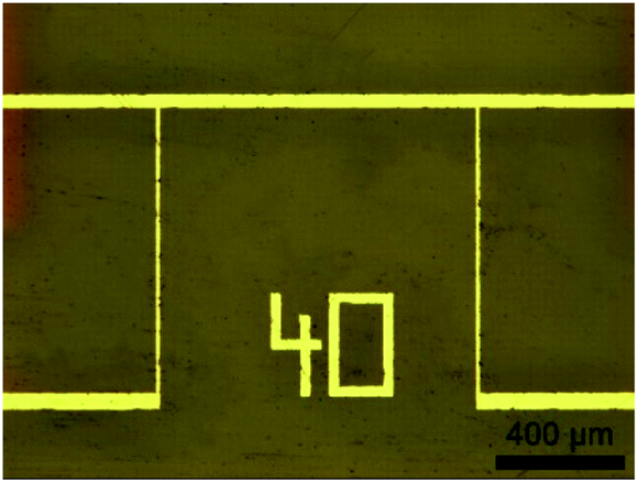 | ||
| Fig. 1 Optical microscopy image of patterned Au thin film on silicon substrate. | ||
| Middle-section length (μm) | Line width (μm) | Film thickness (nm) | |
|---|---|---|---|
| Au on glass | 1000 | 40 | 240 ± 4.1 |
| Au on silicon | 1000 | 40 | 46.6 ± 5.8 |
2.2 SThM experiments
 is determined from the measured electrical resistance and the calibrated temperature coefficient of resistance, TCR, of the probe. While AC current is used in Fig. 2 for electrical resistance measurement and for Joule heating of the probe, DC current can be used instead for the same purposes. Using AC current becomes advantageous when the experiment is extended to contact mode in order to allow for the measurement of the DC Seebeck voltage generated at the probe sample contact without interference from the AC excitation signal, as demonstrated in ref. 37. In a typical SThM thermal conductivity measurement the SThM probe is scanned above the center of the gold thin film line and in the active heating mode, where an AC current is applied to the probe. A second probe connected in a parallel circuit with the measurement probe is placed far away and acts as a reference to monitor the ambient conditions.
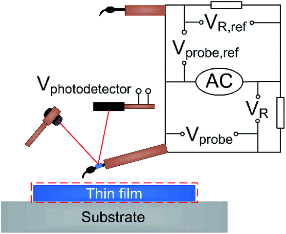 | ||
| Fig. 2 Schematic of the non-contact SThM experimental setup. The voltage signal across the measurement probe (Vprobe), series resistor (VR), reference probe (Vprobe,ref), and reference series resistor (VR,ref) are recorded for thin-film thermal conductivity measurement. The voltage across the photodetector (Vphotodetector) is recorded to control the probe–sample clearance during the experiment. | ||
Fig. 2 shows there are separate channels used to monitor the voltages across each probe and each shunt resistor (2.2 Ω) in the two branches. This allows to monitor the powers dissipated and electrical resistances of the measurement and reference probes independently.
 decreased with decreasing the tip-sample distance while the photodetector signal was constant until the probe contacted the sample surface. At the contact point, there was a voltage jump of the laser detector signal due to the cantilever deflection and a simultaneous sudden temperature drop due to additional solid–solid and water meniscus heat transfer. The photodetector outputted a rising signal and
  was constant after the contact point (see ESI†). The vertical coordinate of the contact point was recorded. The probe was then raised far above the substrate to break the contact. Next, a vertical scanning for thermal resistance measurements was started with the sample 800 nm away from the determined probe–sample contact point. The probe signals were collected after each vertical step size of 100 nm and the last point before contact was referred to as the non-contact point used for data analysis. At each vertical position, the input AC voltage at a frequency of 6 kHz was ramped and the probe thermal resistance was measured. The distance from the non-contact point to the sample is 100 ± 50 nm with the uncertainty caused by the step size. The vertical scanning experiment for thermal resistance measurements was repeated several times.
 | (1) |
 is probe average temperature rise above ambient and P is the Joule heating power.
  is determined from the measured electrical resistance and the calibrated temperature coefficient of resistance, TCR, of the probe. When the probe is close to the sample,
  decreases due to the increasing heat transfer from the probe to the sample under the same input power, leading to a reduction of probe thermal resistance. A three-dimensional finite element model (3DFEM) was developed and used to model the probe–sample-ambient heat transfer, aid in the data analysis of the thin film thermal conductivity, and investigate the influence of clearance on Rthp.
3. 3DFEM for probe–sample-ambient heat transfer
A 3-dimensional Finite Element Model (3DFEM)38 resembling the SThM experimental configuration of the probe was developed. It includes the heat transport processes and geometry of the essential elements e.g. probe, sample, and ambient air. A Wollaston probe is placed with the plane of its V-shaped tip region normal to the sample surface in a configuration similar to the micrograph shown in Fig. 3. This is the only probe–sample angle configuration used in this work. The 3DFEM simulation considers the system at the center of an air box, which is a cube with side of 5 cm. The surface of the air box and the two ends of the V-shaped microprobe are set to constant room temperature as the cold bath. Probe parameters are summarized in Table S1 (see ESI†). The 3DFEM was performed in the DC heating regime since AC temperature rise in our probe is negligible at the high frequency used for the AC current,37 and the experiment monitors the DC temperature change of the probe.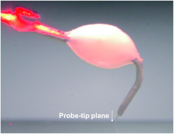 | ||
| Fig. 3 The micrograph of a Wollaston wire probe in the proximity of a sample surface. The plane of the probe tip is normal to the sample surface. | ||
In general, the heat conduction between the probe, the sample, and the surrounding air, and the Joule heating of the probe are all presented in the form of the heat diffusion equation,
| −∇⋅(k∇T) = Q | (2) |
| Q = J2⋅ρ0(1 + TCRp(T − Tref)) | (3) |
The initial temperature was set to Tref = 299.05 K for all the computational domains. Mesh independence studies were conducted with 12![[thin space (1/6-em)]](https://www.rsc.org/images/entities/char_2009.gif) 956804, 14636046, 16348113, 17039584 and 20286444 triangular meshes, respectively. Since the difference of computation results (probe thermal resistance) from 14636046 meshes to 17039584 meshes was only in the order of 1 × 10⁻⁵, 16348113 meshes were chosen.
956804, 14636046, 16348113, 17039584 and 20286444 triangular meshes, respectively. Since the difference of computation results (probe thermal resistance) from 14636046 meshes to 17039584 meshes was only in the order of 1 × 10⁻⁵, 16348113 meshes were chosen.
Since the tip-sample clearance at the apex (50–150 nm) is on the same order as the MFP of ambient air, particular attention is given to modeling the heat transfer in the air gap between the Wollaston probe tip and sample surface to accurately capture the heat transfer in the transition regime. Similar to the method used in ref. 32, the air gap at the probe apex is discretized in concentric cylindrical sections as shown in Fig. 4a. Each section is then assigned an effective thermal conductivity according to its local tip-sample clearance Di and a thermal conductivity model for heat conduction in transition regime,42–44
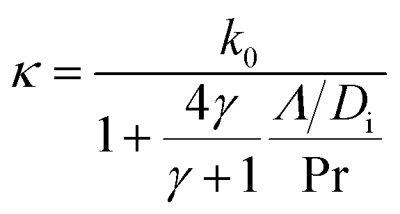 | (4) |
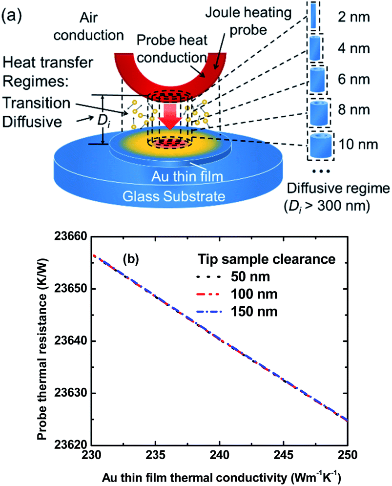 | ||
| Fig. 4 (a) Schematic showing decomposition of probe–sample air gap used for 3DFEM. In the transition regime, eqn (4) is used to assign the effective thermal conductivity of each discretized cylindrical layer based on its local probe–sample clearance; (b) 3DFEM simulations of the probe thermal resistance above a Au film sample (same geometry shown in Table 1) on a glass substrate as a function of thin film thermal conductivity, when the apex tip-sample clearance is 50–150 nm. The curves overlap due to the transition heat conduction regime across apex tip-sample clearances which are similar to the mean free path of the air. | ||
In 3DFEM the probe thermal resistance is obtained by taking the ratio of volumetric averages of probe temperature rise and its thermal power where the probe power is the same as the thermal power in the SThM experiment. Fig. 4b shows a comparison between 3DFEM predictions of Rthp for apex tip-sample clearances of 50 nm, 100 nm, and 150 nm and as a function of thin film thermal conductivity for a 240 nm film on the glass substrate.
The overlapping profiles indicate the gap-independence of Rthp when apex tip-sample clearance is in the transition regime, similar to the experimental results shown in ref. 31. Thus, small fluctuations of apex tip-sample clearance should cause negligible uncertainties (∼0.2%) onto the value of Rthp.
4. Results and discussion
4.1 Thin film thermal conductivity measurements by SThM
Fig. 5 shows experimental probe thermal resistances as a function of apex tip-sample clearance for two Au film samples on glass and silicon substrates. The values of the non-contact Rthp used for data analysis are collected at 100 nm tip-sample clearance and are 23640 ± 9.3, 23778 ± 18 K W−1 respectively, for the films on the glass and silicon substrates. The Rthp of the silicon dioxide film on the silicon substrate is 23941 ± 4.0 K W−1 (see ESI†).
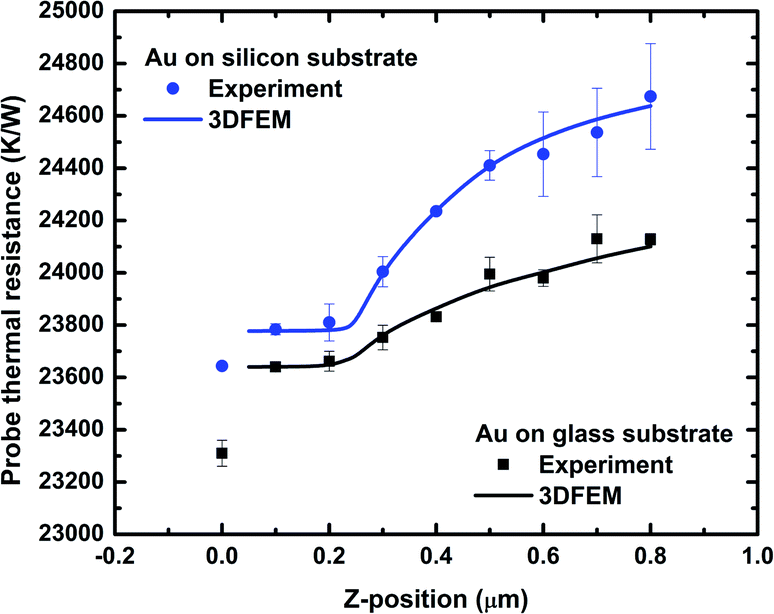 | ||
| Fig. 5 Probe thermal resistance vs. apex tip-sample clearance for Au thin films on silicon and glass substrates from the experiments and 3DFEM simulations. The non-contact thermal resistance is measured at an apex tip-sample clearance of 100 ± 50 nm. The error bars are (max − min)/2 that are calculated based on four separate scanning experiments. The 3DFEM simulations are performed using the fitted values of the film thermal conductivities as measured at 100 nm tip-sample clearance (Table 2). The simulations indicate good agreement with measurements over the entire range of tip-sample distance. | ||
The comparisons shown in Fig. 5 between the experimental probe thermal resistance and 3DFEM predictions indicate that the discrepancy between the experiment and modeling is within the uncertainty of the experimental results. The 3DFEM simulations are performed using the fitted values of the film thermal conductivities based on the probe thermal resistances measured at 100 nm tip-sample distance (the values reported in Table 2). An abrupt change occurs in the trend of the probe thermal resistance vs. position at distances <300 nm because the transition heat conduction in the tip-sample gap starts to become important. The numerical simulations predict an invariant probe thermal resistance in the 50–200 nm height interval which practically eliminates effects due to height uncertainty (see ESI†).
If the heat flow into the sample is low because the sample has a high thermal resistance, the probe remains at a high temperature and results in a higher Rthp. Although the Si substrate with SiO2 film has a lower thermal resistance than the glass substrate, the overall higher probe thermal resistance in Fig. 5 shown for Au on Si sample indicates that the probe–sample heat transfer mainly depends, as discussed later, on the in-plane film thermal resistance and the Au film on Si substrate sample has a higher thermal resistance than the Au film on glass substrate due to the much smaller film thickness.
The jump of the Rthp from non-contact point to contact point is caused by the additional solid–solid conduction and conduction through the water meniscus. According to ref. 31 and 45, the jumps of the probe thermal resistance were observed to be smaller for samples with smaller thermal conductivities, which implied a dependence of solid–solid heat conduction on sample thermal conductivities and surface artifacts. Thus, the smaller jump for the Au on Si substrate sample shown in Fig. 5 may be a result of less heat transfer through the solid–solid heat conduction. More importantly, the non-contact experimental Rthp in Fig. 5 remains almost constant in the transition regime (for the range between 100–200 nm tip-sample clearance at apex), which means it is solely correlated to the sample thermal properties rather than contact artifacts. The probe thermal resistance value at the tip-sample clearance of 100 nm is fitted with 3DFEM simulations in order to obtain the thermal conductivity of the thin film sample. The example in Fig. 6 shows 3DFEM simulations of Rthp performed as a function of kf. By locating the value of the experimental Rthp on the 3DFEM curve, the experimental thin film thermal conductivity was obtained. The red solid line indicates the average thin film thermal conductivity and the red dotted line shows the upper and lower boundaries of the experimental uncertainties of the measured film thermal conductivity due to the uncertainties in the probe thermal resistance. The results for Au thin film thermal conductivity are summarized in Table 2. 3DFEM of the Au film on glass substrate shows that the dominant thermal transport during our experiments is in the radial direction. This is due to the spreading effect of a large thermal conductivity film deposited on a low thermal conductivity substrate (see ESI†). A similar configuration occurs for the Au film deposited on a low thermal conductivity silicon dioxide layer (see ESI†). Therefore the thermal conductivity measurements reported here for the Au films are for in-plane thermal conductivity. The measured thermal conductivity of silicon dioxide film is 1.19 W m−1 K−1 and has a maximum discrepancy of 3.48% vs. the literature values.46,47 For the silicon dioxide film, the dominant thermal transport is in cross-plane direction (see ESI†).
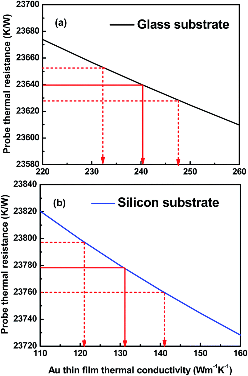 | ||
| Fig. 6 3DFEM predictions of Rthpvs. thermal conductivity of the thin film on (a) glass and (b) silicon substrates with 100 nm apex tip-sample clearance. Using the values of the experimental Rthp the thermal conductivities and uncertainties of the thin films are determined by fitting, as shown by the red arrows. | ||
5. k f validations by Wiedemann–Franz law and theoretical modeling
The Wiedemann–Franz law states that the ratio of thermal conductivity and electrical conductivity at a given temperature is constant for a metal since electrons are the primary carriers for both thermal energy and charge. As a result, the film thermal conductivity can be determined from eqn (5) using bulk thermal and electrical conductivities from ref. 33 and 48, and the experimental thin film electrical resistivity.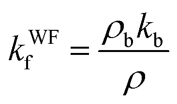 | (5) |
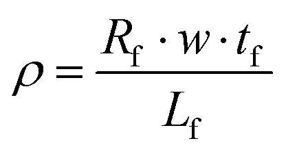
The electrical resistivity was measured using the four-probe setup shown in Fig. 7. The thin-film line was connected electrically in series with an 11.2 Ω resistor. A small DC current (1.5 mA) was applied to the Au thin film to minimize Joule-heating induced resistance change. The voltage drop on the middle section of the line was collected along with the voltage on the series resistor to determine the sample's electrical resistance (Rf). Since the full geometry of the sample is known (Table 1), the electrical resistivity (ρ) of the thin film can be calculated from,
 | (6) |
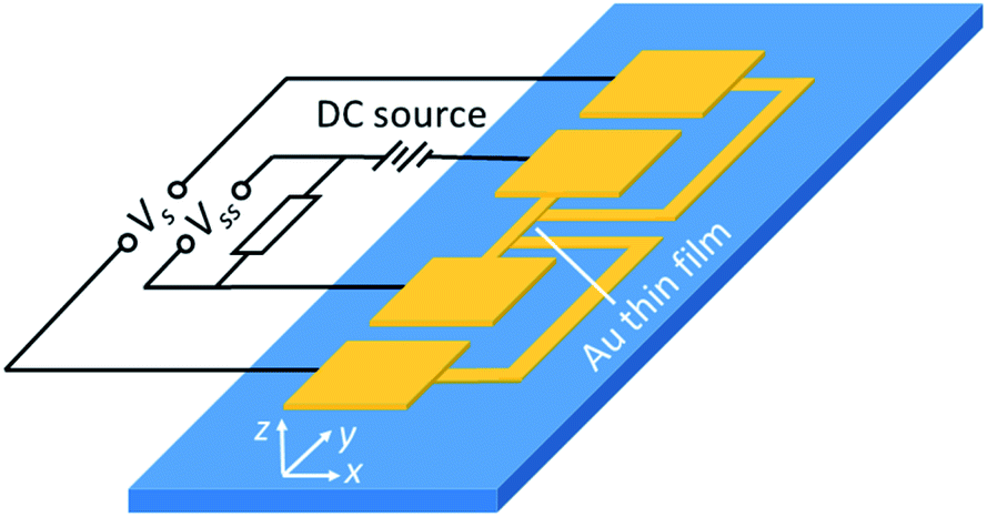 | ||
| Fig. 7 Schematic of thin-film line instrumented for four-probe electrical resistance measurement. The voltage across the thin film line Vs and known series resistor Vss yields the patterned line electrical resistance from which the thin film electrical resistivity is determined. | ||
A summary of the Wiedemann–Franz law validation results is shown in Table 2. SThM thermal conductivity measurements for both Au films agree very well with the thermal conductivity results from Wiedemann–Franz law, with a maximum discrepancy of 6.4%.
A theoretical model for in-plane thin-film thermal conductivity based on kinetic theory was proposed by Qiu and Tien,36
 | (7) |
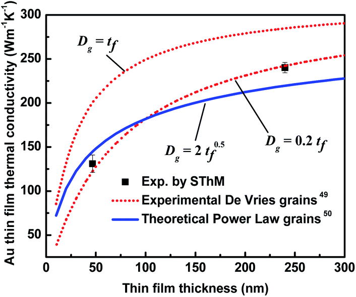 | ||
| Fig. 8 Comparisons between the SThM experimental results (dots) and theoretical model predictions (lines) for thin film thermal conductivity based on ref. 36. Theoretical predictions employ two grain size models, De Vries49 and Power law.50 | ||
Qiu and Tien's theoretical model helps to explain the physical mechanisms responsible for the observed thickness dependence of kf for the Au metallic thin films investigated in this work. For the 240 nm film l/tf and l/Dg are 0.171 and 0.854 respectively, which makes the contribution of grain size the dominant term in eqn (7). For the 46.6 nm film l/tf and l/Dg are 0.88 and 4.40 respectively, which also makes the contribution of grain size the dominant term in eqn (7). When comparing the two thin films, the reduction of thickness likely created smaller size grains and the additional scattering of the heat carriers resulted in lower in-plane thermal conductivity.51 Similar size effects have been observed for other types of 2D materials using different measurement techniques.41,52
6. Analytical heat conduction modelling
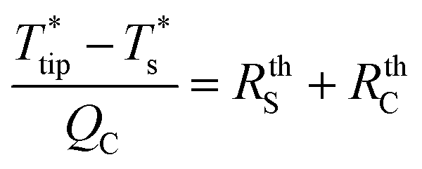
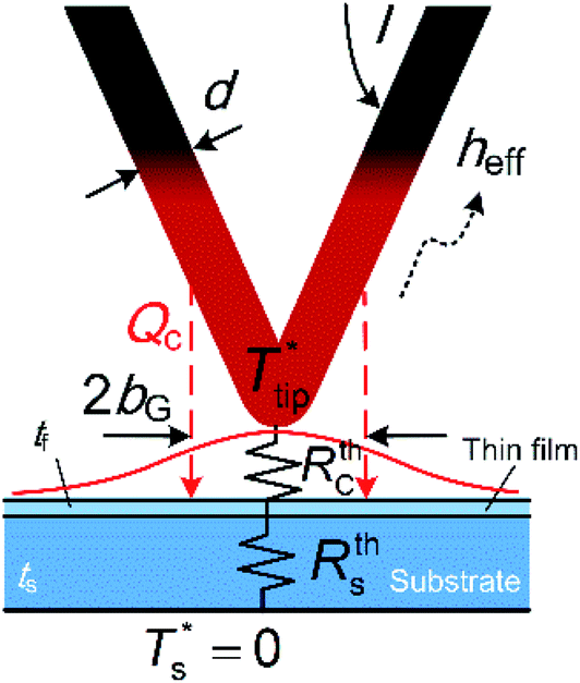
To reduce the time and complexity of data analysis and facilitate experimental investigations and planning in the absence of 3DFEM, an analytical model was developed for the thermal transport between the Wollaston probe and film-on-substrate samples under ambient conditions. 3DFEM was employed though to validate the analytical model assumptions and assess the accuracy of thin-film thermal conductivity determination based on analytical modeling.The thermal model shown in Fig. 9 is used to connect into a thermal resistance network all three heat transfer domains (probe, sample, ambient), and includes models for the thermal resistances of the probe, the air gap, and the film-on-substrate thermal resistances. An analytical model for a self-heated Wollaston probe in air with the probe–sample heat transfer confined to the apex region was developed in ref. 12 and 31, but for different sample configurations than used in this work (for substrate only samples in ref. 30, and for film-on-substrate samples where heat transfer is assumed unidirectional along the film thickness direction in ref. 12). For the Wollaston probe, the model solves a 1D fin heat conduction equation along the length of the Joule heated probe wire to obtain the temperature rise at probe apex ( ) as a function of probe geometry, probe thermal properties, effective heat transfer coefficient h and tip-sample heat transfer rate (QC). In this analytical model a correlation is employed for the tip-sample thermal exchange resistance (RthC) as a function of thermal exchange radius b, probe–sample clearance and probe wire diameter, which was developed in ref. 32 for a Wollaston probe in air. This correlation considers both the classical and non-classical heat conduction effects in the small tip-sample air gap. Then, using the heat transfer rate QC through the tip-sample thermal resistance network and the tip to back-of-substrate temperature difference, the sum of the tip-sample thermal exchange resistance with the thermal resistance of the film-on-substrate sample (RthS) can be written as,
 | (8) |
 .
.
 | ||
| Fig. 9 Schematic of the probe–sample system used for the analytical modeling of the probe–sample-ambient heat transfer. | ||
For large thermal conductivity films on low thermal conductivity substrates, in-plane heat conduction is expected to be significant and the model developed in ref. 12 and 19–21 will not apply for the sample configurations measured here. The key challenge remaining for the analytical model is then finding an analytical thermal resistance model for the film-on-substrate sample (RthS), when in-plane heat conduction in the film is significant.
In order to better understand the distribution of heat flux on the sample surface, results from 3DFEM heat transfer simulations of the probe–sample-ambient system were first used to calculate the surface heat flux spatial profile due to SThM probe heating of a thin film-on-substrate sample. Although the geometry of a Wollaston SThM probe is not axisymmetric, the sample surface heat fluxes probed along two perpendicular directions in the plane of the sample (one parallel and one perpendicular to the plane of the SThM probe defined by its V-shape) were found to have similar Gaussian radii which are independent of the tip-sample distance when this is in 100–300 nm range (see ESI†). The characteristic radius of the heat flux Gaussian profile bGC was then taken as the square root of the product of the two Gaussian radii (bG). Thus, an analytical model developed for Gaussian laser heating of a multilayer film-on-substrate configuration6 was adapted here to determine the thermal resistance of film-on-substrate samples in general, and was exemplified here for thin films on glass substrate and on silicon substrate with an interfacial SiO2 film.
6.1 Analytical model for the thermal resistance of thin film-on substrate samples
As shown in the previous section, in Fig. 9 the heating effect from the non-contact SThM probe was replaced by a heat flux with a Gaussian heating distribution acting on the top surface of the thin film. A multilayer anisotropic heat conduction model with Gaussian heating boundary condition was developed in ref. 6, and was adapted here to the case of a three-layer isotropic structure consisting of the thin-film layer, the SiO2 interface layer and the substrate layer. The bottom of the substrate can be assumed either thermally insulated or isothermal. For the substrates investigated in this work the results are practically identical (<0.21% discrepancy on sample temperature for film thickness ≤540 nm) and the solution below assumes adiabatic condition at the substrate bottom. The temperature is assumed to reach the ambient temperature as r goes to infinite along the direction of the radius. The objective is finding the thermal resistance of the sample.Based on ref. 6, the governing equation for steady-state heat conduction in the thin film and substrate, assuming isotropic thermal properties and no temperature gradients in the azimuthal direction is given by eqn (9):
 | (9) |
Then, with the boundary conditions described in Section 12 of the ESI,† the steady-state solution for the temperature distribution on the thin film surface can be obtained by Hankel transformation in terms of the Hankel variable β as,
 | (10) |
 is the transformed Gaussian heat flux,
 | (11) |
 | (12) |
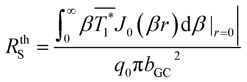 | (13) |
The value of the thermal resistance calculated from eqn (13) is independent of the peak flux. The temperature profile predicted by the analytical model was cross-validated by 3DFEM for the same sample geometry (see ESI†) using the Gaussian heat flux profile determined from 3DFEM. The thermal resistance discrepancy calculated from the analytical and 3DFEM models was within 0.4%.
The probe tip temperature rise 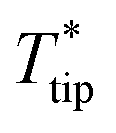 can be determined from the analytical model of the Wollaston wire probe with circular cross-section and neglecting radiative heat loss as shown in eqn (14)–(16)12,29,32,53
 | (14) |
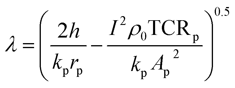 | (15) |
 | (16) |
The expressions for C3 and C4 and the values12,28,31,52 used for h, kp, Ap, rp, TCRp, I, and ρ0 (effective heat transfer coefficient, thermal conductivity of the probe, cross-sectional area of the probe, radius of the probe, thermal coefficient of resistance, applied current and reference electrical resistivity of the probe respectively) are found in the ESI.† As the Wollaston probe comes closer to the surface, the effective heat transfer coefficient is still applied to the probe surface, except in the region undergoing heat transfer to the sample through the thermal exchange area. Eqn (17) connects the probe tip temperature rise to ambient temperature via the RthC and RthS, where RthS is based on eqn (13) and RthC is a function of b according to the correlation developed in ref. 32.
 | (17) |
The analytical model assumes that the thermal exchange radius (b) of the probe is the same as bGC. This assumption was validated (see ESI†) by 3DFEM of the SThM sample system with bulk samples for kb = 1.1–50 W m−1 K−1 and finding b = bGC = 5.4 μm ± 0.1 μm. Then (see ESI†) it was found that bG for the thin film-on-substrate sample is also almost unchanged when kf ranges from 10 to 1000 W m−1 K−1 for tf = 240 nm and ks = 1.1 W m−1 K−1. It was concluded that b = bGC = 4.6 μm ± 0.1 μm for thin film-on-glass samples.
Using the tip-sample thermal exchange resistance correlation developed in ref. 52, the sample–probe thermal exchange resistance at the tip-sample clearance of 100 nm yields RthC of 126626 K W−1 for b = 4.6 μm. The unknown kf can be then obtained based on eqn (17) by numerically fitting kf as ks, tf, ts, b and RthC are known.
The lateral spatial resolution in SThM measurements using heated probes is indicated by the diameter of the heat diffusion region in the sample, resulting from the heat transfer between the heated probe and the sample. This region is ultimately limited by 2b, the diameter of the probe–sample thermal exchange area,25 which is typically considered the limit of the spatial resolution. For contact mode SThM performed under ambient conditions, air conduction contributes significantly to the probe–sample heat transfer (∼10 μm thermal exchange diameter for a Wollaston probe22) and therefore the spatial resolution of the contact mode may not be significantly smaller than in non-contact mode.54 The spatial resolution of SThM non-contact mode in air is controlled by the dimension and geometry of the probe tip. Smaller probe tips will generally have a smaller thermal exchange radius. For SThM experiments performed under vacuum conditions, the thermal exchange area for contact mode is controlled by the solid–solid contact area and thus results in an improved spatial resolution.4
6.2 Analytical model validation and tf·kf fitted functions development
To validate the analytical heat transfer model for the SThM measurements shown in Fig. 9, 3DFEM was used first to determine the probe thermal resistance for various thin film thermal conductivities for a disk-shaped thin film on a glass substrate sample. The value of the probe thermal resistance was used next to perform data analysis using the analytical model. The value of b = bGC = 4.6 μm was initially used by the analytical model. The was obtained from probe's analytical model, and with RthC = 126626 K W−1 for b = bGC = 4.6 μm, then the unknown kf was determined by fitting eqn (13) and eqn (17). The fitted kf from the analytical model was compared to the input kf of 3DFEM. The values of kfvs. Rthp for different tf are plotted and compared in Fig. 10a. The maximum discrepancy between the analytical result and the true value of kf is less than 34% if kf is between 100–700 W m−1 K−1 for thin film thickness between 50–300 nm. A lower discrepancy of <9.4% is obtained in the range of 200–500 W m−1 K−1 for kf and 240–300 nm for tf. When multiplying tf with kf from Fig. 10a, and replotting their product vs. Rthp the obtained curves are almost overlapping for both the analytical model and 3DFEM as shown in Fig. 10b. Similar to the trends shown in Fig. 10a, a larger discrepancy of tf·kf is observed at higher kf.
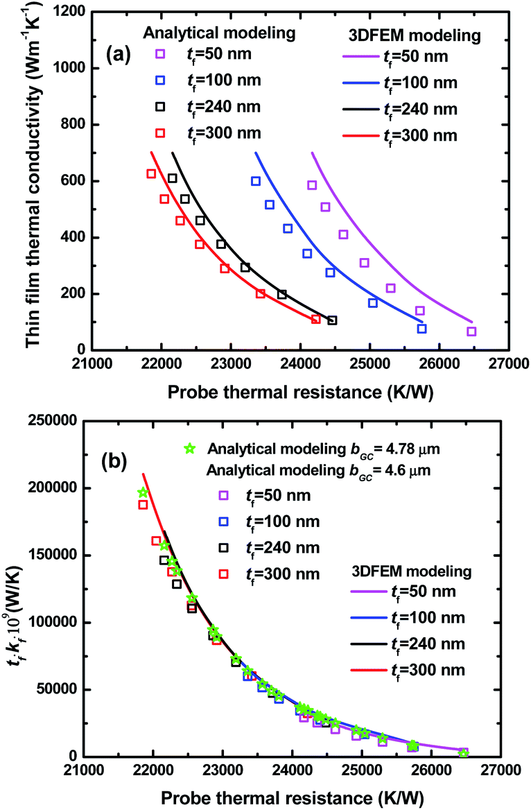 | ||
| Fig. 10 Comparisons shown as a function of probe thermal resistance predicted from 3DFEM for films on glass substrate with tf from 50–300 nm and kf from 50–600 W m−1 K−1: (a) between the actual kf values used in the 3DFEM and the kf obtained by fitting with analytical models; and (b) between the actual product of tf with kf and the product of tf with kf obtained by fitting with analytical models. | ||
Based on the data from Fig. 10b, three numerical correlations were developed by fitting the 3DFEM and analytical results for tf·kf (m W m−1 K−1) vs. Rthp (K W−1) with eqn (18).
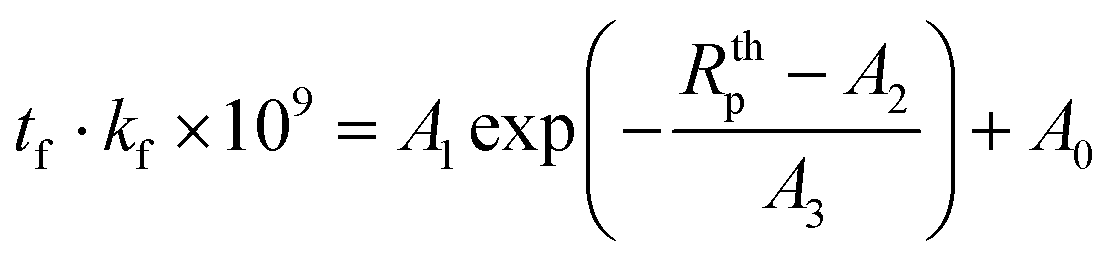 | (18) |
The fitted parameters in eqn (18) and the goodness of fit are summarized in Table 3 for each case. Plots comparing the 3DFEM and analytical results from Fig. 10bvs.eqn (18) fits are shown in ESI.†
| AM bGC = 4.6 μm | 3DFEM | AM bGC = 4.78 μm | |
|---|---|---|---|
| A1 | 190848.80 |
210153.80 |
201554.71 |
| A2 | 21855.57 |
21850.29 |
21847.14 |
| A3 | 1424.99 | 1265.99 | 1406.76 |
| A0 | −5318.05 | 822.06 | −3804.22 |
| R | 0.99919 | 0.99951 | 0.99974 |
Using the experimentally obtained probe thermal resistance for the measured sample and eqn (18) fit of the analytical model with b = bGC = 4.6 μm, the kf of Au film on glass substrate was calculated as 205.2 W m−1 K−1, which has a 10.6% discrepancy compared to kWFf shown in Table 2. Using eqn (18) fit of the 3DFEM yields kf = 216.4 W m−1 K−1 which has a 5.7% discrepancy compared to kWFf shown in Table 2. The deviation from the 3DFEM simulation result from Fig. 6a is due to the different geometry of the film used in the modelling (patterned line vs. un-patterned film). If the 3DFEM results on glass substrate (Fig. 10b) are used to re-calibrate the value of b in the analytical model, then b = 4.78 μm. Then the discrepancy between the 3DFEM result and the result obtained using eqn (18) fitted function of the analytical model with the new b reduces to 0.8%.
The kf for the Au film on the silicon substrate sample can be quickly evaluated using a fitted function developed by fitting the three-layer analytical model predictions (see ESI†). The fitted kf = 116.6 W m−1 K−1 for the gold film on silicon substrate using this fitted function has a 16.7% discrepancy compared to the kWFf shown in Table 2.
While the data analysis based on 3DFEM provides the most accurate thermal conductivity measurement results, fitted functions avoid repeating the 3DFEM simulations for films deposited on the same substrates. The fitted functions reported in this work provide faster ways to perform data analysis or investigate feasibility of future experiments for films deposited on the two types of substrates investigated here. For films deposited on different substrates or for different probe geometries, the experimentalist has to find the new fit functions. Moreover, analytical modelling can prove useful (vs. 3DFEM and developed fitted functions) due to its speed and flexibility, for instance, new fitted functions can be developed faster based on analytical modeling for cases when the probe has different dimensions or thermal properties that are different from those used in this work, or for films on other types of substrates, or if the sample configuration requires additional layers to be added to the 3-layer model developed in this work. Then 3DFEM and fit-functions based on 3DFEM can be used for fine-tuning or validating the final thermal conductivity result.
7. Conclusions
In conclusion, a quantitative method was established to measure thin film thermal conductivity in non-contact mode in ambient conditions and in transition heat conduction regime across the tip-sample gap. With the help of 3DFEM for data analysis, the thermal conductivities of Au thin films deposited on the glass and silicon substrate were measured as 240.2 ± 5.9 W m−1 K−1 and 131.0 ± 9.9 W m−1 K−1 respectively. The validation by experimental electrical resistivity measurements using Wiedemann–Franz law and in addition by theoretical thermal conductivity modeling (Qiu and Tien) showed a maximum deviation of less than 6.4% from SThM experimental results. While the 3DFEM based modelling provides the most accurate thermal conductivity measurement results, convenient fitted functions for SThM on the film-on-substrate sample were developed by the recalibrated analytical model and 3DFEM to assist in fast and accurate (<16.7% discrepancy compared to experimental values) thin film thermal conductivity measurements for ∼50–300 nm films deposited on glass and Si substrates with 100 < kf < 600 W m−1 K−1. The analytical models developed here for measurements on one-film and two-films on substrate samples can prove useful (vs. 3DFEM and developed fitted functions) due to their adaptability when sample configuration or probe parameters change.Conflicts of interest
There are no conflicts to declare.Notes and references
- X. Zhang and L.-D. Zhao, J Materiomics, 2015, 1, 92–105 CrossRef.
- S. Gomès, A. Assy and P.-O. Chapuis, Phys. Status Solidi A, 2015, 212, 477–494 CrossRef.
- G. Wielgoszewski and T. Gotszalk, Adv. Imag. Electron. Phys., 2015, 190, 177–221 Search PubMed.
- Y. Zhang, W. Zhu, F. Hui, M. Lanza, T. Borca-Tasciuc and M. M. Rojo, Adv. Funct. Mater., 2020, 1900892, 1–33 Search PubMed.
- T. Borca-Tasciuc and G. Chen, Int. J. Thermophys., 1998, 19, 557–567 CrossRef CAS.
- T. Borca-Tasciuc, D. Borca-Tasciuc and G. Chen, IEEE Trans. Compon. Packag. Technol., 2007, 30, 609–617 CAS.
- J. L. Battaglia, A. Kusiak, C. Rossignol and N. Chigarev, J. Phys. Conf. Ser., 2007, 92, 012083 CrossRef.
- A. Rosencwaig and A. Gersho, J. Appl. Phys., 1976, 47, 64–69 CrossRef.
- K. Goodson and M. I. Flik, Appl. Mech. Rev., 1994, 47, 101–112 CrossRef.
- A. Majumdar, Annu. Rev. Mater. Sci., 1999, 29, 505–585 CrossRef CAS.
- E. N. Esfahani, F. Ma, S. Wang, Y. Ou, J. Yang and J. Li, Natl. Sci. Rev., 2018, 5, 59–69 CrossRef CAS.
- A. Wilson, M. Rojo, B. Abad, J. Perez Taborda, J. Maiz, J. Schomacker, M. Martín-González, D.-A. Borca-Tasciuc and T. Borca-Tasciuc, Nanoscale, 2015, 1–3 Search PubMed.
- J. Perez Taborda, M. Rojo, J. Maiz, N. Neophytou and M. Martín-González, Sci. Rep., 2016, 6, 32778 CrossRef CAS.
- J. Perez Taborda, O. Caballero-Calero, L. Vera-Londono, F. Briones and M. Martín-González, Adv. Energy Mater., 2018, 17020241 Search PubMed.
- J. Bodzenta, J. Juszczyk, A. Kaźmierczak-Bałata, P. Firek, A. Fleming and M. Chirtoc, Int. J. Thermophys., 2016, 37, 17 CrossRef.
- A. Kaźmierczak-Bałata, J. Bodzenta, M. Krzywiecki, J. Juszczyk, J. Szmidt and P. Firek, Thin Solid Films, 2013, 545, 217–221 CrossRef.
- S. Lefevre and S. Volz, Rev. Sci. Instrum., 2005, 76, 033701 CrossRef.
- S. Lefevre, J. B. Saulnier, C. Fuentes and S. Volz, Superlattices Microstruct., 2004, 35, 283–288 CrossRef CAS.
- J. L. Battaglia, A. Saci, I. De, R. Cecchini, S. Selmo, M. Fanciulli, S. Cecchi and M. Longo, Phys. Status Solidi A, 2017, 214, 1600500 CrossRef.
- J. L. Battaglia, A. Kusiak, V. Schick, A. Cappella, C. Wiemer, M. Longo and E. Varesi, J. Appl. Phys., 2010, 107, 044314 CrossRef.
- A. Cappella, J.-L. Battaglia, V. Schick, A. Kusiak, A. Lamperti, C. Wiemer and B. Hay, Adv. Eng. Mater., 2013, 15, 1046–1050 CrossRef CAS.
- A. M. Massoud, J. M. Bluet, V. Lacatena, M. Haras, J. F. Robillard and P. O. Chapuis, Appl. Phys. Lett., 2017, 111, 063106 CrossRef.
- A. Wilson, MRS Commun., 2019, 9, 650–656 CrossRef CAS.
- W. Jeong, K. Kim, Y. Kim, W. Lee and P. Reddy, Sci. Rep., 2014, 4, 4975 CrossRef CAS.
- K. Kim, W. Jeong, W. Lee and P. Reddy, ACS Nano, 2012, 6, 4248–4257 CrossRef CAS.
- Y.-J. Yu, M. Y. Han, S. Berciaud, A. B. Georgescu, T. Heinz, L. E Brus, K. Kim and P. Kim, Appl. Phys. Lett., 2011, 99, 183105 CrossRef.
- L. Shi, J. Zhou, P. Kim, A. Bachtold, A. Majumdar and P. McEuen, J. Appl. Phys., 2009, 105, 104306 CrossRef.
- P.-O. Chapuis, J.-J. Greffet, K. Joulain and S. Volz, Nanotechnology, 2006, 17, 2978 CrossRef CAS.
- T. Borca-Tasciuc, Annu. Rev. Heat Transfer, 2013, 16, 211–258 CrossRef.
- F. Menges, P. Mensch, H. HSchmid, H. Riel, A. Stemmer and B. Gotsmann, Nat. Commun., 2016, 7, 1–6 Search PubMed.
- Y. Zhang, E. Castillo, R. Mehta, G. Ramanath and T. Borca-Tasciuc, Rev. Sci. Instrum., 2011, 82, 024902 CrossRef.
- Y. Zhang, W. Zhu, L. Han and T. Borca-Tasciuc, Rev. Sci. Instrum., 2020, 91, 014901 CrossRef CAS.
- G. Chen and P. Hui, Appl. Phys. Lett., 1999, 74, 2942–2944 CrossRef CAS.
- F. Völklein, H. Reith, T. W. Cornelius, M. Rauber and R. Neumann, Nanotechnology, 2009, 20, 325706 CrossRef.
- X. Zhang, C. Bingyang, M. Fujii and K. Takahashi, Phys. Rev. B: Condens. Matter Mater. Phys., 2006, 74, 134109 CrossRef.
- T. Q. Qiu and C. L. Tien, J. Heat Transfer, 1993, 115, 842–847 CrossRef CAS.
- Y. Zhang, C. Hapenciuc, E. Castillo, T. Borca-Tasciuc, R. Mehta, C. Karthik and G. Ramanath, Appl. Phys. Lett., 2010, 96, 062107 CrossRef.
- C. Multiphysics, COMSOL multiphysics user guide (Version 4.3a), COMSOL, 2012 Search PubMed.
- J. Bodzenta, J. Juszczyk and M. Chirtoc, Rev. Sci. Instrum., 2013, 84, 093702 CrossRef CAS.
- R. H. Perry and D. W. Green, Perry's Chemical Engineers' Handbook, 7th edn, McGraw-Hill, 1997 Search PubMed.
- W. Jang, Z. Chen, W. Bao, J. Lau and C. Dames, Nano Lett., 2010, 10, 3909–3913 CrossRef CAS.
- M. Calvert and J. Baker, J. Thermophys. Heat Transfer, 1998, 12, 138–145 CrossRef CAS.
- C.-Y. Zhu, Z.-Y. Li and W.-Q. Tao, J. Heat Transfer, 2017, 139, 052405 CrossRef.
- W. D. Zhou, B. Liu, S. K. Yu and W. Hua, Phys. Rev. E - Stat. Nonlinear Soft Matter Phys., 2010, 81, 011204 CrossRef CAS.
- A. A. Wilson, Analysis of non-contact and contact probe-to-sample thermal exchange for quantitative measurements of thin film and nanostructure thermal conductivity by the scanning hot probe method, PhD dissertation, Rensselaer Polytechnic Inst., Troy, New York, 2017.
- M. G. Burzo, P. L. Komarov and P. E. Raad, IEEE Trans. Compon. Packag. Technol., 2003, 26, 80–88 CrossRef CAS.
- O. W. Käding, H. Skurk and K. E. Goodson, Appl. Phys. Lett., 1994, 65, 1629–1631 CrossRef.
- R. A. Matula, J. Phys. Chem. Ref. Data, 1979, 8, 1147–1298 CrossRef CAS.
- J. W. C. De Vries, Thin Solid Films, 1988, 167, 25–32 CrossRef CAS.
- Z. L. Wu, P. K. Kuo, W. Lanhua, S. L. Gu and R. L. Thomas, Thin Solid Films, 1993, 236, 191–198 CrossRef CAS.
- G. Langer, J. Hartmann and M. Reichling, Rev. Sci. Instrum., 1997, 68, 1510 CrossRef CAS.
- I. Jo, M. T. Pettes, J. Kim, K. Watanabe, T. Taniguchi, Z. Yao and L. Shi, Nano Lett., 2013, 13, 550–554 CrossRef CAS.
- A. Wilson and T. Borca-Tasciuc, Rev. Sci. Instrum., 2017, 88, 074903 CrossRef.
- F. Menges, H. Riel, A. Stemmer and B. Gotsmann, Nano Lett., 2012, 12, 596–601 CrossRef CAS.
Footnote |
| † Electronic supplementary information (ESI) available: eqn (S1-S5) and Table S1: supplemental equations and coefficients for the analytical model of the active probe and values for Wollaston probe parameters. Fig. S1: Comparison of temperature profiles predicted by 3DFEM and analytical models. Fig. S2: Gaussian fitting of surface heat flux along different directions. Fig. S3: Gaussian fitting of surface heat flux for different bulk samples. Fig. S4: Gaussian fitting of surface heat flux for different films. Fig. S5: Gaussian fitting of surface heat flux for different probe-sample distances. Fig. S6: Probe thermal resistance and measured thermal conductivity for a silicon dioxide film on silicon substrate. Fig. S7 and S8: Comparisons between data and fitted functions of the product between film thickness and thermal conductivity vs. probe thermal resistance for Au on glass and Au on Si substrate samples, respectively. Fig. S9: photodetector signals for Au on glass and Si substrate samples. Fig. S10: Heat flux ratio (in-plane vs. cross-plane) for the thin film samples. Fig. S11: Optical microscopy image of the probe and 3DFEM temperature distributions for the Wollaston probe–air–sample system. Eqn (S7-S13): Boundary conditions for the analytical model of the film-on-substrate sample. See DOI: 10.1039/d0na00657b |
| This journal is © The Royal Society of Chemistry 2021 |