
 Open Access Article
 This Open Access Article is licensed under a Creative Commons Attribution-Non Commercial 3.0 Unported Licence
Innovative PIN-type perovskite solar cells with 17% efficiency: processing and characterization†
T.
Lemercier
ab,
L.
Perrin
 a,
S.
Berson
b,
L.
Flandin
a and
E.
Planes
*a
a,
S.
Berson
b,
L.
Flandin
a and
E.
Planes
*a
aUniv. Grenoble Alpes, Univ. Savoie Mont Blanc, CNRS, Grenoble INP, LEPMI, 38000 Grenoble, France. E-mail: emilie.planes@univ-smb.fr
bUniv. Grenoble Alpes, CEA, LITEN, INES, 73375 Le Bourget-du-lac, France
First published on 4th October 2021
Abstract
To develop high-performance tandem cells, it seems necessary to optimize semi-transparent PSC single junctions with a PIN-type architecture. In this article, the development of this PIN-type architecture by the optimization of the Hole Transport Layer (HTL) is proposed. Firstly a study of three HTLs with different surface properties such as PEDOT:PSS, PTAA and TFB was carried out, to understand their influence on the deposition conditions and on the final properties of the deposited perovskite layer. Indeed, the use of layers such as PTAA and TFB represents a real alternative, already mentioned as very promising in NIP and PIN type architectures. But unlike PEDOT:PSS, these hydrophobic layers disrupt the deposition of the perovskite layer. Once the material was chosen the HTL, here TFB, which has real originality, the optimization of the process was carried out. The latter based on the evaluation of the antisolvent ejection time and the drying time allowed a drastic increase in the PCE from 10% to 17%. Another important result of this study is the methodology used for this optimization. Indeed, the main marker used is the observation of defects in the perovskite layer at the macroscopic and microscopic scales. This optimization of the perovskite layer morphology leads to a significant increase in performance. This approach will be very useful to the community for a possible optimization of other devices.
Introduction
Perovskite materials have been widely developed in the photovoltaic (PV) field for a few years.1 These materials, processed at low temperatures, present exceptional optoelectronic properties.2 A wide bandgap range (from 1.17 to 3.11 eV)3 combined with an excellent mobility4 and very good absorption properties5 make them the materials of choice for PV tandem architectures,6,7 in particular with silicon solar cells. The main objective is to exceed the Shockley–Queisser efficiency limit.8Two different architectures can be used for perovskite solar cells (PSCs), depending on the order of the layer deposition, with a hole or an electron transport layer (HTL or ETL), underneath the perovskite. The NIP-type architecture is the most common because it was easier to process at the first stage of perovskite PV and led to the first PV yields with a TiO29 based ETL. The first PIN-type structures appeared for a second time with PEDOT:PSS10 as the HTL. Today, both architectures achieved high efficiencies in the range of 20–22%,11,12 but the NIP-type architecture has led to the record efficiencies for single junction cells.11 In comparison, somewhat lower efficiencies are consistently obtained for PIN-type architectures.13
In the case of a monolithic tandem application combining perovskite and silicon solar cells, the highest efficiencies are obtained with perovskite cells in the PIN-type architecture.14 The latter allows the reduction of parasitic absorption at the front side of the device, compared to the NIP-type architecture.15 A thin (despite absorbing) N-type interface within the PIN-type architecture (e.g. C60 layer) appears indeed to be optically less detrimental than the thick highly absorbing HTL typically employed in the standard one (e.g. spiro-OMeTAD).14 To develop high-performance tandem cells, it therefore seems to be necessary to optimize semi-transparent PSC single junctions with the PIN-type architecture. This type of cell is gradually more studied, and the efficiencies increased accordingly up to 17%.16–21 The performances depend essentially on the materials used as active and interfacial layers. The main weakness of these architectures is the lower value of Voc, due to the use of non-suitable N- and P-type interfacial layers. This prevents the optimal operation of the perovskite layer and favors the radiative recombination.22
The current work focuses on the development of innovative PIN-type perovskite solar cells. For this, we propose to use mixed perovskites, which present several advantages over the most common form MAPbI3 (with MA = methylammonium). The multiple cation/anion perovskites lead to higher yields, and better stability and reproducibility.23,24 In addition, controlling the stoichiometry in mixed perovskites (especially the iodide/bromide ratio) allows adjustment of the bandgap energy of the material in view of a tandem application.25 An FA1−yCsyPb(I1−xBrx)3 (with FA = formamidinium) perovskite has recently been developed with a formulation specifically optimized for the development of low-temperature perovskite devices in the NIP-type architecture.26 The optimum ratios were found to be 88% for I/Br and 94% for FA/Cs. This previous work suggested good potential of this formulation for both efficiency and stability. To improve the performances of these devices and in particular their Voc, it is also proposed to study several HTLs with very different surface properties, PEDOT:PSS, PTAA and TFB, in order also to understand their influence on the deposition and on the properties of the perovskite layer deposited afterwards. Indeed, the use of layers such as PTAA and TFB represents a real alternative, already mentioned as very promising in both NIP- and PIN-type architectures.27–29 But unlike PEDOT:PSS, these hydrophobic layers disturb the deposition of the perovskite layer. Several approaches are proposed in the literature to improve the wettability of the perovskite on these hydrophobic layers,30,31 but it is preferable to preserve the nature of the materials, and quite possible to optimize the quality of the perovskite layer by solely varying the processing conditions. We propose here double optimization of the material and process to maximize the PCE of the devices. The main originality concerning the material concerns the use of TFB as the HTL. To vary the processing, a combined optimization of the antisolvent ejection time and the drying time before annealing was performed. These two steps permitted a drastic increase in the PCE from 10% to 17%. In addition, comprehensive elements are provided to broaden the experimental conclusions, and unravel new process/microstructure/properties of the perovskite. This will be very useful to the community for a possible optimization of other devices.
Experimental part
The preparation of perovskite solutions, fabrication of solar devices and their photovoltaic characterization were carried out in a glove box containing less than 1 ppm oxygen and moisture.Materials
All anhydrous solvents (dimethylformamide (DMF), dimethylsulfoxide (DMSO), chlorobenzene (CB), o-xylene, ethyl acetate (EA), diethyl ether (DE) and isopropanol (IPA)) were purchased from Sigma Aldrich, as were PbBr2, CsI and PTAA. PbI2 was purchased from Tokyo Chemical Industry and formamidinium iodide (FAI) from Greatcell Solar Materials. PEDOT:PSS and TFB were respectively purchased from Heraeus (ref. Clevios P-VPAI-4083) and American Dye Source (ref. ADS259BE). Np-SnO2 (a dispersion of nanoparticles at 2.5 wt% in butanols (20.7 mg mL−1)) was purchased from Avantama (ref. N30) and PC60BM from Merck (ref. Lisicon PV-A600). Silver used for metallic contacts was purchased from Neyco, and the ITO coated substrates (square resistivity of 7 Ω/□) from Visiontek (ref. ITOGLASS 07P).Solar cell preparation
The perovskite precursor solution of FACsPbBrI at 0.87 or 1.15 mol L−1 (for lead) was made in a glovebox from the three following intermediate solutions: a perovskite precursor solution of FAPbI3 at 0.87 or 1.15 mol L−1 (lead) prepared with FAI![[thin space (1/6-em)]](https://www.rsc.org/images/entities/char_2009.gif) :PbI2 at a 1.05:1 molar ratio in DMF:DMSO at 4:1 in volume, stirred one night at 40 °C; a 0.87 or 1.15 mol L−1 PbBr2 solution in DMF:DMSO at 4:1 in volume, also stirred one night at 40 °C; and a 1.5 mol L−1 CsI solution in DMSO, stirred at room-temperature. The three intermediate solutions were mixed for about 30 min before use (during which the final solution was cooled down to room temperature).
:PbI2 at a 1.05:1 molar ratio in DMF:DMSO at 4:1 in volume, stirred one night at 40 °C; a 0.87 or 1.15 mol L−1 PbBr2 solution in DMF:DMSO at 4:1 in volume, also stirred one night at 40 °C; and a 1.5 mol L−1 CsI solution in DMSO, stirred at room-temperature. The three intermediate solutions were mixed for about 30 min before use (during which the final solution was cooled down to room temperature).
ITO coated substrates were sonicated sequentially in acetone, isopropanol and eventually deionized water. Before the first deposition layer, these substrates were treated with UV-ozone for 30 min. For PTAA as the HTL, the layer was deposited by spin-coating in a glovebox from a solution at 2 mg mL−1 in chlorobenzene, filtered using a 0.45 μm PTFE filter, and then dried at 110 °C for 10 min. For PEDOT:PSS as the HTL, the layer was deposited by spin-coating in air from a commercial solution, filtered using a 0.45 μm GMF w/GMF filter, and then dried at 180 °C for 1 hour in an oven. For TFB as the HTL, a very thin layer, from a solution at 0.6 mg mL−1 in o-xylene, was deposited by spin-coating in a glovebox and then dried at 150 °C for 10 min. In order to suppress possible macroscopic defaults, a surface treatment by DMF was applied onto PTAA and TFB right before the perovskite layer deposition. The previously described perovskite precursor solution, filtered using a PTFE filter of 0.45 μm, is then spread and spin-coated, where XX ∈ {10, 20, 30, 40, 50, 60} s. 150 μL of ethyl acetate are used as antisolvent and poured on the perovskite layer 5 s before the end of the spin-coating program (tASE = XX − 5 s). Afterwards, the resulting perovskite layer is dried at room temperature in a glovebox for 0 or 20 min (tDBA), and finally annealed at 80 °C for 1 h. After the samples were cooled down, around 20 nm of PCBM are then deposited by spin-coating, from a 10 mg.mL-1 concentrated solution in chlorobenzene, filtered with a PTFE filter of 0.45 μm. No drying or annealing was performed after PCBM deposition. 50 μL of np-SnO2 at 2.5 wt% in butanols, previously filtered with a PP w/GMF filter of 0.45 μm, was finally deposited by dynamic spin-coating by means of an electronic pipette, leading to a thickness of about 20 nm. Dynamic spin-coating was chosen for minimizing the contact time between the solvent of np-SnO2 (butanols) and the perovskite. No drying or annealing was performed after np-SnO2 deposition. 100 nm of silver were deposited by thermal evaporation under vacuum to complete the setup, delimitating an active area of 0.34 cm2.
Characterization
Photocurrent–voltage (J–V) curves were generated in a glovebox with a solar simulator (Newport Oriel SP94043), calibrated using a silicon reference solar cell at a light intensity of 100 mW cm−2. A voltage sweep from 2.5 V to −0.2 V (reverse scan) with a step of 0.1 V and 20 ms of acquisition time for each data point was the parameter used for the J–V measurements. They were performed every minute for at least 15 min under illumination for each cell to reach stabilization of their efficiency. All the UV-visible characterization studies were performed in air using a UV-visible spectrophotometer (UV-2600, Shimadzu, Japan) with an integration sphere. X-ray diffraction (XRD) patterns were collected in air using a Malvern PANalytical apparatus (Aeris version) equipped with an X-ray source (λ(Kα) = 0.178901 nm), a divergence slit of ½°, an angle aperture of 0.04 rad and a 23 mm beam mask. Photoluminescence (PL) spectra were obtained with a fluorescence spectrophotometer (Hitachi F-4500 FL, Hitachi, Japan) with an excitation wavelength of 467 nm (corresponding to the highest intensity response) and a speed sweep of 1200 nm min−1 (an excitation slit of 10.0 nm, an emission slit of 20.0 nm and a photomultiplier tube voltage of 400 V). A set of two filters was used to remove the 2θ harmonics and instrumental artifacts: a low-pass filter at 575 nm upstream and a high-pass filter at 600 nm downstream. For this experiment, the samples were only composed of the perovskite layer and the underlying HTL deposited on the glass/ITO substrate. The thicknesses were estimated with a profilometer (D500, KLA Tencor, USA) after scratching the upper layers, with the following parameters: a displacement speed of 0.05 mm s−1, an equivalent strength of 1 mg, and the height range of 10 μm. Work functions were acquired in air at room-temperature and in the dark using a Kelvin probe from KP Technology equipped with a digital control setup managed by Kelvin probe measurement system version DELTA software. During acquisitions, the oscillation frequency of the tip was set to 96 Hz, with an amplitude of 38 V, an electromotive force of ±7 V, a trigger probe of 114 counts, and with an electrostatic force gradient of 300 N m−1. For samples with perovskite, 300 consecutive measurements in one location were realized. Copper tape was used to guarantee the electrical contact between samples and the sample holder of the Kelvin probe. The tip work function was deduced by using a thermally evaporated gold layer of 100 nm. To establish the experimental standard deviation and the average work function of gold in air (attributed to −4.7 eV),32 100 consecutive measurements were achieved at three different locations of the gold layer before and after samples’ measurement campaigns. Images from optical microscopy were acquired with a Leica DMLM microscope and a Leica DFC420 camera, in transmission for orange-like images and in reflection for blue-like images with a ×10 magnification. Picture analysis was performed with ImageJ. Analyses to evaluate the microscopic pinholes’ surface percentage were conducted with ImageJ software on 3 different pictures for each condition: pictures are set in the greyscale image at first, then a threshold is applied to settle and distinguish pinholes in the layer, and the binarization function is lastly applied to the image before extracting the surface area corresponding to the pinholes. SEM images were acquired using a Nova NanoSEM 630 apparatus equipped with secondary electron detectors, with a working distance of around 5 mm and a voltage of 7 kV.Results and discussion
The present study focuses on the development of PIN solar cells, with a specific goal to upgrade the perovskite layer on an innovative and promising HTL. Fig. 1a presents the architecture of the studied cell. A mixed perovskite with two cations and two anions serves as the active layer. Its chemical structure (CH(NH2)2)(1−y)CsyPb(I(1−x)Brx)3 will be simplified as (FACsPbIBr). This complex stoichiometry results from the iterative optimization from different studies to favor yields, stability and robustness.23,24 For instance, as the energy bandgap depends on the molar ratios of the different species, the stoichiometry may be used as a means to customize the materials and match the desired absorption. This may help to reach a variety of specific needs. For tandem25 applications, the iodine to bromine ratio is commonly modified to optimize the bandgap of the subcell to be combined with the silicon one. The addition of cesium (Cs) in the structure allows improvement of the stability of the crystalline structure of the brominated and iodinated perovskites.33 The presence of Cs hinders the formation of the photo-inactive delta phase (δ-FAPbI3).26,33 To facilitate the processing and improve the stability,34 the perovskite structure without methylammonium may be formulated with formamidinium and cesium. The performance (higher than 12%) and stability recently obtained with these types of perovskite in NIP-type architectures are satisfactory.26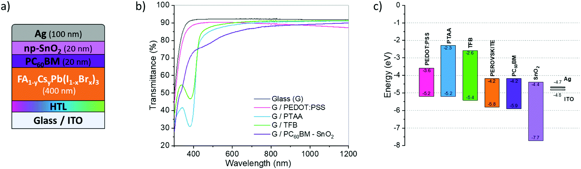 | ||
| Fig. 1 Structure and properties of the solar cells developed in the present study. (a) PIN-type architecture on the ITO coated glass substrate; (b) optical properties in transmission of studied HTLs and ETL; and (c) energy levels of the constitutive materials (data issued from the literature). | ||
The PCBM/BCP layer is intensively used for its efficiency in opaque PIN-type cells,22,35,36 and alternatives are also being investigated for tandem application.7,37 PCBM combines a good stability with a strong ability to extract electrons from the perovskite layer,38,39Fig. 1c. It may safely be kept in the final architecture. In contrast, the BCP layer should be replaced by a more robust one. The substitution material ideally combines the roles of the buffer and hole blocking layer,35 in addition to the ability to develop a good interface with the metal (low resistance and ohmic behavior). We decided to focus on SnO2 that has already been identified among the best buffer layers and ETL.40 Here a SnO2 layer based on nanoparticles has been used. A preliminary study was thus carried out to stack PCBM and SnO2 in order to optimize the two thicknesses with regard to the overall PCE (presented in Fig. S1, ESI†). This means that the best optical and physical properties compromise for a semi-transparent application.
Different HTLs were investigated including PEDOT:PSS, PTAA and TFB. For PIN-type architectures, PEDOT:PSS's hydrophilic character and its excellent wettability for the perovskite precursor solutions facilitate the processing of the active layer.41,42 Unfortunately, the resulting cells present low Voc, due to their greater ability to form recombinant traps at the HTL/perovskite interface.43 Other alternative materials have been tested, among which PTAA was considered a most promising candidate. It combines excellent optical properties and work function but its hydrophobicity limits the wettability of the perovskite layer. TFB was also considered because the latter presents an even better energy level alignment with perovskite, due to its lower HOMO level value close to 5.4 eV. This should induce an improvement of the Voc, Fig. 1c. TFB also shows better electronic mobility than PTAA, while keeping similar and excellent optical properties,30,44Fig. 1b. However, TFB is hydrophobic in nature such as PTAA, and a dedicated protocol should be developed for these HTLs to obtain a homogeneous and controlled morphology of the perovskite layer.
To improve the wettability of the perovskite on the highly hydrophobic organic HTL, prior surface treatment with DMF allows avoiding macroscopic holes (as observable in Fig. 2b). The use of an anti-solvent should also be necessary to obtain a good quality and covering layer.45 In the case of a NIP architecture, the perovskite deposition is done on a rather hydrophilic layer (TiO2, SnO2) and chlorobenzene is generally used as an anti-solvent. In the case of deposition on hydrophobic layers (PTAA and TFB), the nature of the anti-solvent largely affects the quality of the deposited perovskite layer. As shown in Fig. S2 (ESI†) and Fig. 2a, the use of diethyl ether (DE) here leads to a macroscopically non-compliant perovskite layer, and the use of the common chlorobenzene (CB) leads to large holes of about 30 μm without perovskite and the HTL beneath, indicating the dissolution of the latter, as also observed in the literature31 and confirmed by the test presented in Fig. S2 (ESI†). Although the use of other anti-solvents leads to more homogeneous deposits, microscopic observations show much smaller pinhole diameters (less than 15 μm, and without any HTL dissolution) in the case of ethyl acetate (EA) and isopropanol (IPA). Such an effect of the nature of the anti-solvent has already been observed in the literature, but generally at a lower scale.46,47 IPA and EA appear here to be the best candidates. Our choice turned to EA because of literature results that show higher yields in single junctions48 and tandem cells,15 in contrast to IPA which is known to easily solubilize the organic compound of the perovskite material.49 EA is by the way reported to offer a better moisture resistance during perovskite fabrication.50
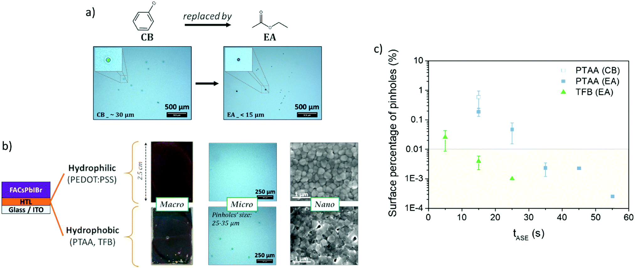 | ||
| Fig. 2 (a) Impact of anti-solvent's nature (chlorobenzene vs. ethyl acetate) on the micro-scale pinholes in the perovskite layer (examples on the PTAA layer, tASE = 15 s); (b) impact of the HTL nature (hydrophilic vs. hydrophobic) on the perovskite layer at macro-, micro- and nano-scales (examples with EA, tASE = 15 s); and (c) surface pinhole proportion (determined by optical microscopy, see Fig. S3, ESI†) as a function of anti-solvent ejection time (tASE) and HTL nature. | ||
Without changing the nature of the materials, the quality of the deposited layer may be largely altered by varying the processing conditions. For instance, adjusting the anti-solvent ejection time (tASE) seems interesting:51–54 the principle is presented in Fig. 3. The latter has hardly been used, mainly for the mono-cation perovskite (MAPbI3). The authors concluded that the tASE influences the absorbance and crystallinity of the perovskite. The optimisation of the tASE can thereby significantly improve the performances of the solar cells, although in a phenomenological manner exclusive to each specific system. Y. Bai et al. revealed an optimum in the PCE yields as a function of the tASE for different perovskite formulations. They proposed a much longer optimal time (40 s51) than previous studies (10 s53 or even 5 s52). As presented in Fig. 2b, with an anti-solvent ejection time ≤15 s, micro-scale holes and nano-scale defects are visible in the case of hydrophobic HTLs like PTAA and TFB. Such defects are not observable in the case of the PEDOT:PSS-based HTL, confirming the role played by the nature of the HTL surface. As suggested in the literature, we varied the ejection time between 5 and 55 s and observed the obtained perovskite layers with an optical microscope (Fig. S4, ESI†). After image analysis (ImageJ), the relative number of micro-pinholes within the surface was calculated and plotted as a function of the anti-solvent ejection time, Fig. 2c. For the two hydrophobic layers studied (PTAA and TFB), this proportion of defects decreases significantly with the ejection time, together with the average diameter of the holes. This improvement is much faster with TFB, for which no microscopic defects remain after only 15 s, compared to 35 s with PTAA.
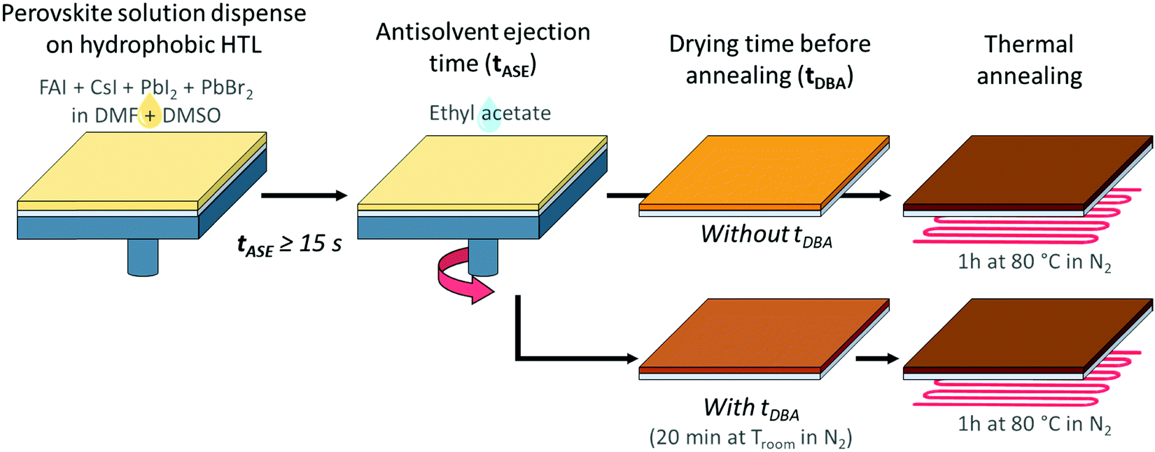 | ||
| Fig. 3 Illustration of the deposition process for the perovskite layer on an HTL with the two studied parameters: the anti-solvent ejection time (tASE) and the drying time before annealing (tDBA). | ||
To better understand the effect of this anti-solvent ejection time, the perovskite layer deposited on the three HTLs was analyzed by X-ray diffraction and UV-Visible absorption spectroscopy. The X-ray diffraction pattern of the active layer for tASE is shown in Fig. S5 (ESI†). The diffraction peak located at 2θ close to 12.7° is commonly attributed to the PbI2 phase.55 The presence of bromine in the formulation can lead to PbX2, generally detected at 2θ close to 13.1–13.2°.22,56 The presence of PbI2 was further confirmed by 25.7° and 38.9° peaks characteristic of the second- and third-order of the diffraction pattern. The other peaks could be attributed to the perovskite FA1−yCsyPb(I1−xBrx)3. Various crystal orientations are observed, mainly (00![[small script l]](https://www.rsc.org/images/entities/char_e146.gif) ) for which three orders of diffraction are detected at 14.1° (001), 28.4° (002) and 43.1° (003). Other orientations can also be detected (see details in the ESI†). The solution of perovskite precursors was formulated as FA0.94Cs0.06Pb(I0.88Br0.12)3. The formed perovskite phase will be referred to as FACsPbIBr in the following. It has a cubic structure like FAPbI3,3,57 with peaks slightly shifted towards larger angles. This is due to the reduction of the lattice plan associated with the presence of the smaller bromine atoms in the formulation, as compared to iodine. Finally, a small amount of the photo-inactive and undesirable δ-FAPbI3 phase is detected at 2θ of 11.7–11.8°.58
) for which three orders of diffraction are detected at 14.1° (001), 28.4° (002) and 43.1° (003). Other orientations can also be detected (see details in the ESI†). The solution of perovskite precursors was formulated as FA0.94Cs0.06Pb(I0.88Br0.12)3. The formed perovskite phase will be referred to as FACsPbIBr in the following. It has a cubic structure like FAPbI3,3,57 with peaks slightly shifted towards larger angles. This is due to the reduction of the lattice plan associated with the presence of the smaller bromine atoms in the formulation, as compared to iodine. Finally, a small amount of the photo-inactive and undesirable δ-FAPbI3 phase is detected at 2θ of 11.7–11.8°.58
As expected, all the tested tASE promote the nucleation and growth of the same few crystal phases (FACsPbIBr, PbI2 and δ-FAPbI3), Fig. S5 (ESI†). From a quantitative standpoint the proportions of pertinent phases such as FACsPbIBr, PbI2 and δ-FAPbI3 were evaluated with the anti-solvent ejection time tASE, Fig. 4. For the three HTLs studied, the proportion of the FACsPbIBr phase decreases progressively with an increase in tASE from a value of 15 s. Concerning the variations of PbI2, the proportion of this phase follows another trend with a minimum located respectively around 35 s, 15 s and 25 s for respectively PTAA, PEDOT:PSS and TFB. As this compound can have a negative effect on the functioning of the cell, it seems necessary to choose deposition conditions that limit it to a maximum. It is therefore possible to define an indicator corresponding to the ratio of FACsPbIBr and PbI2 phases to highlight optimal conditions for the preparation of the perovskite layer. The latter is also maximal for tASE equal to 35 s, 15 s and 25 s, respectively, for PTAA, PEDOT:PSS and TFB. We note for these conditions that the proportion of the δ-FAPbI3 phase is negligible and thus should have little consequence on the functional properties of the perovskite layer.
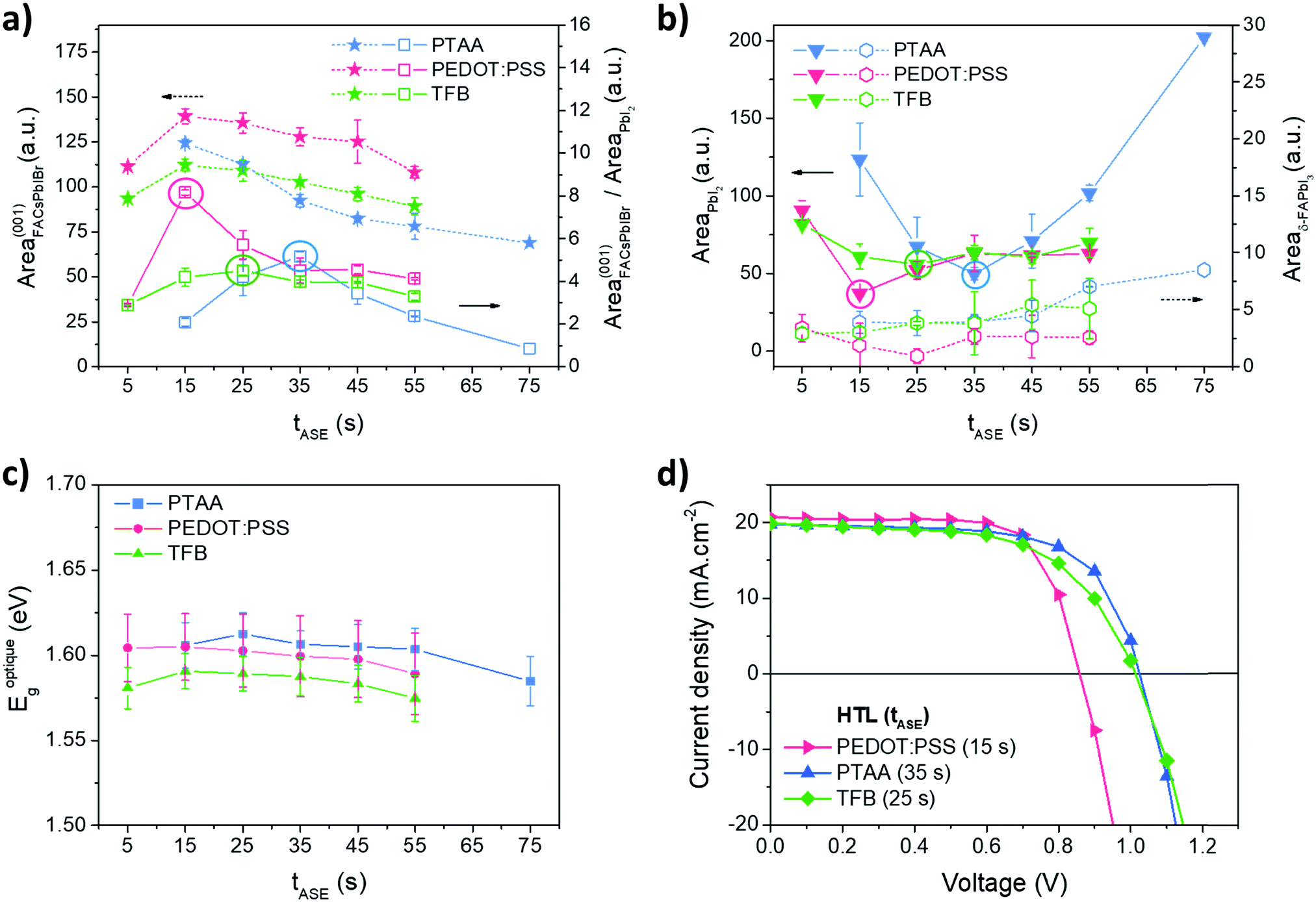 | ||
| Fig. 4 For the three studied HTLs PTAA (blue), PEDOT:PSS (pink), and TFB (green): (a) and (b) extracted areas of the main diffraction peaks attributed to the FACsPbIBr (along the orientation (001)), PbI2 and δ-FAPbI3 phases, and the areas ratio of the FACsPbIBr (along the orientation (001)) and PbI2 phases as a function of tASE; (c) optical bandgaps determined by the Tauc plot method as a function of tASE; and (d) J–V measurements in reverse scan of solar cells based on PEDOT:PSS, PTAA and TFB with respectively a tASE of 15 s, 35 s and 25 s. | ||
The optical properties were also investigated by UV-Visible spectroscopy. The raw data obtained are presented in Fig. S6 (ESI†) and the bandgaps, calculated from the Tauc plot method, in Fig. 4c. The optical properties are not much altered by tASE: negligible variations in the optical bandgap and in absorbance magnitude. The bandgaps are however slightly different depending on the HTL, respectively, 1.58 eV, 1.60 eV and 1.61 eV for TFB, PEDOT:PSS and PTAA.
The optimal tASE determined by XRD analyses has been tested in solar cells: the corresponding J–V measurements and PV parameters are shown in Fig. 4d and Table 1. Efficiencies of around 12% are obtained for cells based on PEDOT:PSS and PTAA. The TFB leads to somewhat lower efficiencies, closer to 11%. The FF values are rather good, around 60% for PTAA and TFB and above 70% for PEDOT:PSS. The values of Jsc are similar regardless of the HTL studied and close to 20 mA cm−2 which is in agreement with the literature. The most interesting result concerns the values of Voc. As expected and demonstrated in the literature,59 this is below 1 V for PEDOT:PSS, while an increase towards 1 V is obtained for the other two HTLs. The work function of PEDOT:PSS probably does not match well with that of the perovskite absorber.60 However these values remain a little low compared to those obtained in the literature,61–63 and it seems that our systems can still be improved.
| HTL | V oc (V) | J sc (mA cm−2) | FF (%) | PCE (%) | R s (Ω cm2) | R oc (Ω cm2) | R sc (Ω cm2) |
|---|---|---|---|---|---|---|---|
| a Perovskite concentration = 0.87 mol L−1. b Perovskite concentration = 1.15 mol L−1. | |||||||
| PEDOT:PSSa | 0.86 ± 0.02 | 18.8 ± 1.3 | 73 ± 5 | 11.7 ± 0.8 | 3.5 ± 0.7 | 8.8 ± 1.3 | 11585 ± 37291 |
| (15 s) | (0.85) | (20.4) | (76) | (13.2) | (3.2) | (7.4) | (179025) |
| PTAAa | 1.00 ± 0.03 | 19.8 ± 0.8 | 60 ± 8 | 12.0 ± 1.9 | 2.7 ± 0.2 | 9.1 ± 1.8 | 489 ± 245 |
| (35 s) | (1.03) | (19.5) | (67) | (13.4) | (2.5) | (7.4) | (514) |
| TFBa | 0.91 ± 0.05 | 20.2 ± 0.6 | 56 ± 7 | 10.4 ± 1.6 | 3.6 ± 0.7 | 11.8 ± 3.0 | 446 ± 247 |
| (25 s) | (1.00) | (19.8) | (61) | (12.1) | (3.2) | (9.2) | (589) |
| TFBb | 1.09 ± 0.01 | 20.5 ± 0.5 | 64 ± 3 | 14.3 ± 0.8 | 2.6 ± 0.2 | 9.9 ± 2.6 | 1122 ± 456 |
| (15 s) | (1.08) | (21.2) | (66) | (15.3) | (2.3) | (6.0) | (1370) |
It was further decided to focus the rest of the study on a single HTL. TFB was chosen for its promising character according to the recent results obtained in the literature.51,61,64 It presents notably better properties compared to PTAA such as its mobility (10−2 cm2 V−1 s−1vs. 4 × 10⁻³ cm2 V−1 s−1, according to data from suppliers) and energy levels that more suitable for the architectures tested here.
The optimization of the anti-solvent and its ejection time could not entirely solve the identified issue of pinholes within the perovskite layer, particularly on the microscale and nanoscale (Fig. 2b). In addition, the number of pinholes is not entirely reproducible, meaning that the process could not be totally controlled. It was decided to improve the process by increasing at first the concentration of the perovskite precursor (1.15 mol L−1 instead of 0.87 mol L−1), leading to more reproducible and efficient devices. This also induces an increase in the thickness of the active layer from 250 nm to 400 nm. A proportional increase in absorption is observed below 750 nm and the effect on the optical properties of the devices is negligible for wavelengths targeted for tandem applications (above 800 nm), as shown in Fig. S7 (ESI†). A summary of the corresponding results is presented in Fig. 5. The amount of the crystalline FACsPbIBr phase within the active layer increased for all the tASE tested, Fig. 5a. This proportion seems maximal between 15 s and 25 s of tASE. According to Fig. 5b, the plot of our previously defined indicator thus allows defining an optimal ejection time slightly different from the one previously determined, i.e. close to 15 s. Even if this indicator is slightly lower for this new concentration, the performance in solar cells is better presented in Fig. 5c, indicating a more important effect of the quality and thickness of the deposited perovskite layer than those of its microstructure. These tests in solar cells enable validation of this first optimization phase. As shown in Fig. 5e, we note a further improvement of the Voc after increasing the perovskite precursor concentration and an increase in efficiency from 10% to 14%, Table 1, probably explained by an improvement of the perovskite microstructure.
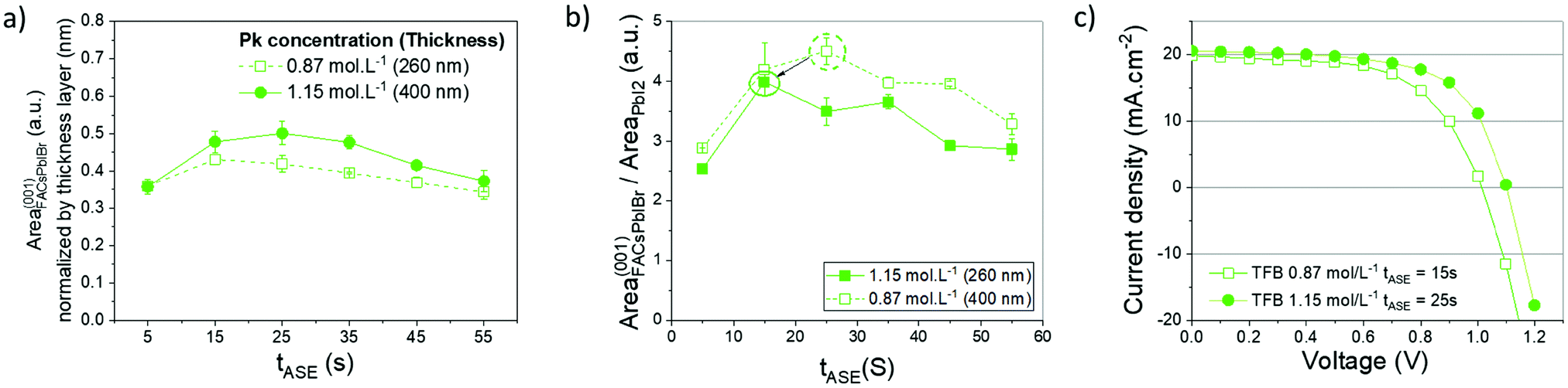 | ||
| Fig. 5 Effect of perovskite concentration, 0.87 mol L−1 (open symbols dashed lines) vs. 1.15 mol L−1 (closed symbols continuous lines), on: (a) extracted areas of the diffraction peaks related to the FACsPbIBr phase according to orientation (001) normalized with the thickness of the perovskite layer as a function of tASE; (b) ratio of FACsPbIBr and PbI2 phases as a function of tASE; and (c) J–V measurements in reverse scan obtained for the 2 concentrations with their respective optimal tASE. | ||
In addition to the anti-solvent, an annealing procedure after the perovskite deposition permits the full conversion of the intermediate perovskite precursors into the desired perovskite and often improves the properties of the perovskite layer, and the overall performance of the cells.65,66 This approach consists in annealing the perovskite layer under milder conditions to avoid a too fast evaporation of the solvents and to obtain a more homogeneous layer at the nanoscale. In the literature, this type of approach has already been encountered essentially for the perovskite of form MAPbI3.67–69 In some studies, this is also carried out with a solvent (or solvent mixtures) to assist the perovskite crystallization during the annealing.65,66,70,71 The nature of the anti-solvent is important, and ethyl acetate (EA) is well-suited for this optimization67,68 for mono- and mixed-cation perovskites.69 The annealing procedure is usually performed in a single step, typically by setting the temperature at 100 °C. The conversion of mixed perovskite has also been reported to possibly occur at room-temperature due to the addition of Cs+ in the perovskite formulation69,72 However, several successive steps including lower intermediate temperature seem to be helpful to obtain higher quality of the perovskite and thus higher device efficiency.73,74 This approach can therefore be particularly applicable to our case study. Here, in the search for the optimisation of the perovskite deposition procedure, we have therefore introduced a drying time before annealing (tDBA, Fig. 3) at room temperature without solvent in order to limit the number of study parameters and to have a greater control of this new process. As illustrated in Fig. S8 (ESI†), we noticed that 20 min tDBA may help to enhance the PCE of our devices. Between 0 and 15 min tDBA, a progressive enhancement in device performances can be observed. After 15–20 min, a plateau is then reached, hence the choice of 20 min was extended in the cases of other tASE. The enhancement magnitude, however, seems dependent on tASE. As a result, the present study deals with the coupled effects of tASE and tDBA upon cell efficiencies and perovskite properties. The goal is thus to optimize the PSCs, and share a way to do so.
The morphological properties of the perovskite layer were studied by scanning electron microscopy (SEM) as a function of tASE duration, as presented in Fig. 6a1, b1, c1 and d. For tDBA = 0 min, the perovskite morphology is characterized by nano-scaled pinholes and grain size ranging between 200 and 300 nm. It appears that the grains are slightly larger after 5 s tASE. This is supported by statistical analysis (Fig. 6d), where the averages of grain size distributions are respectively 250–300 nm (15 s and 35 s) and 200–250 nm (5 s).
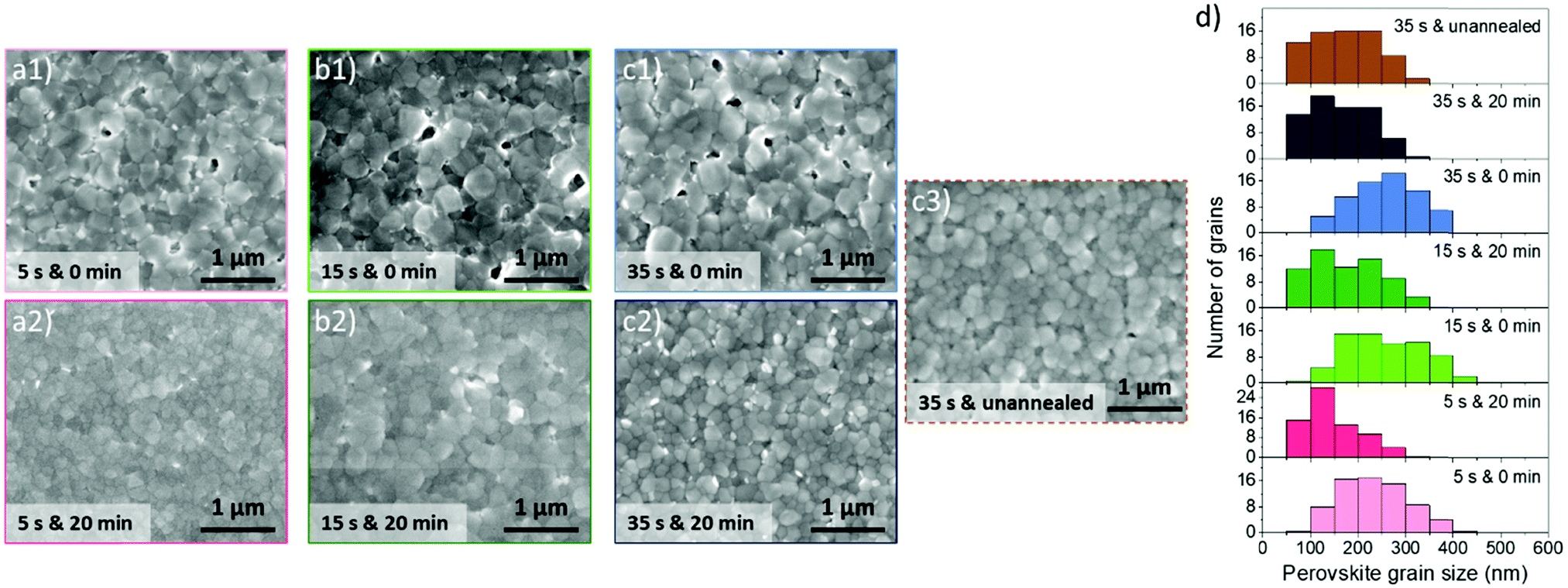 | ||
| Fig. 6 (a)–(c) SEM observations of perovskite layers (performed with a perovskite concentration of 1.15 mol L−1) for different “tASE & tDBA”; and (d) corresponding grain size distributions. | ||
The coupled influence of tASE and tDBA has also been studied, and the corresponding SEM images of the resulting perovskite layer morphology are depicted in Fig. 6a2, b2 and c2. As soon as 20 min tDBA is applied to develop the perovskite layer, the morphology changes significantly whatever tASE is used. We observe that the additional drying step leads to more homogeneous surfaces, without nano-scaled pinholes, also noticeable when no annealing was performed after the drying step, Fig. 6c. This seems to be confirmed by the grain size distributions, which appear to be somewhat wider and show a decrease in the average grain size of around 150 to 250 nm. The introduction of this step leads therefore to perovskite layers with a much more homogeneous and smoother quality from a morphological point of view, which can undoubtedly have positive repercussions on the PV performances of the manufactured cells. Thus the manner in which the perovskite layer crystallizes during the annealing step determines strongly its nanoscale morphology. Therefore, delaying the annealing slows down perovskite layer crystallization, which then allows a better nanoscale morphology. It is believed that crystallization at room temperature affects the diffusion magnitude of perovskite precursors within the “fresh” undried thin perovskite layer (right after the spin-coating step) by slowing it down as well. Perhaps, the mechanism would be similar to the one that occurs when a surfactant is added in the perovskite solution.75
As mentioned in the introduction, the main novelty of this work is the combined study of the effect of the tASE and tDBA parameters on the PV performance of cells. The results relating to PV performances are presented in Fig. 7. Without tDBA, the best performances were reached with the lowest tASE: i.e., 5 s and 15 s (dotted lines in Fig. 7). Average PCEs around 14–15% are obtained for these two conditions. Increasing tASE reduces the performances to about 12%. These variations essentially result from the FF and Voc parameters, Fig. 7 and Table 2. A FF above 60% is measured for tASE of 5 s and 15 s, whereas it is reduced for longer tASE. These observations are compatible with an increase in the series resistance Rs as a function of the tASE, indicating lower effective charge transport through the whole device and likely more specifically between the active layer and the interfacial layers, Table 2. Voc is also larger for shorter tASE and reaches up to 1.09 V, while delaying the ejection of the anti-solvent leads to a Voc reduction of about 0.10 V, Table 2. This may thus also result from an increase in non-radiative recombinations,76,77 as shown in Fig. S9 (ESI†).
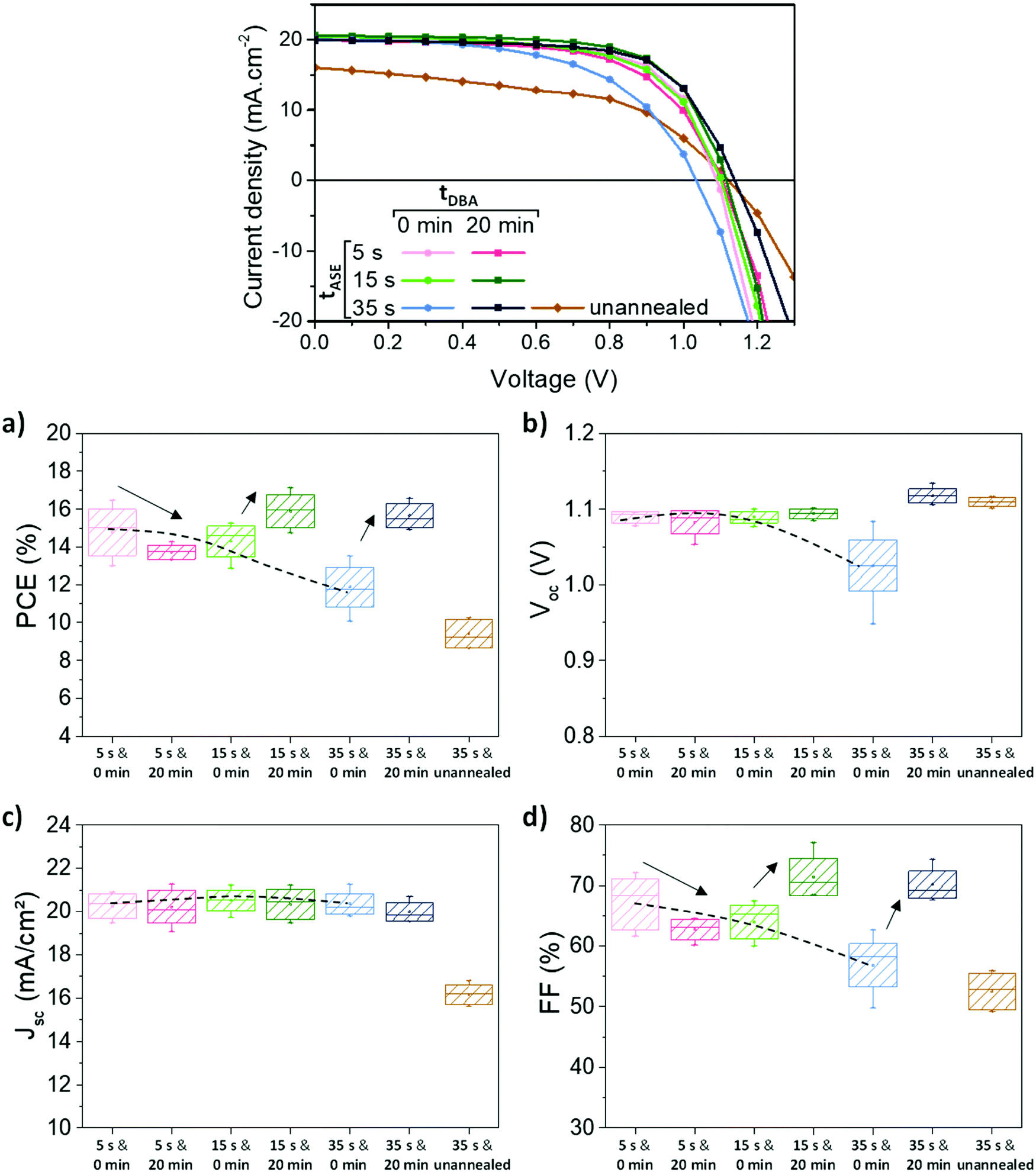 | ||
| Fig. 7 Influence of the processing parameters of the perovskite layer on the device performances. The two durations of tASE and tDBA are varied. (a) Representative J–V measurements in reverse scan, with an active area of 0.34 cm2; means (points), medians (lines), standard deviations (boxes) and minimum–maximum (extrema) of the PV parameters (statistics on 6 to 15 cells): (b) PCE, (c) Voc, (d) Jsc and (e) FF. The dotted lines indicate the trend as a function of tASE, while the effect of tDBA is represented by arrows. | ||
| Conditions | V oc (V) | J sc (mA cm−2) | FF (%) | PCE (%) | R s (Ω cm2) | R oc (Ω cm2) | R sc (Ω cm2) |
|---|---|---|---|---|---|---|---|
| 5 s & 0 min | 1.089 ± 0.008 (1.093) | 20.2 ± 0.6 (20.9) | 67.0 ± 4.2 (72.1) | 14.8 ± 1.2 (16.5) | 2.47 ± 0.24 (2.24) | 8.6 ± 2.7 (5.6) | 934 ± 404 (1644) |
| 5 s & 20 min | 1.083 ± 0.015 (1.095) | 20.2 ± 0.8 (20.8) | 62.8 ± 1.7 (62.8) | 13.7 ± 0.4 (14.3) | 2.39 ± 0.55 (1.98) | 9.7 ± 2.5 (8.3) | 841 ± 436 (1062) |
| 15 s & 0 min | 1.090 ± 0.008 (1.084) | 20.5 ± 0.5 (21.2) | 64.0 ± 2.8 (66.4) | 14.3 ± 0.8 (15.3) | 2.56 ± 0.16 (2.32) | 9.9 ± 2.6 (6.0) | 1122 ± 456 (1370) |
| 15 s & 20 min | 1.094 ± 0.006 (1.097) | 20.3 ± 0.7 (20.2) | 71.4 ± 3.0 (77.1) | 15.9 ± 0.9 (17.1) | 2.32 ± 0.37 (2.30) | 6.9 ± 1.5 (5.1) | 1609 ± 183 (1788) |
| 35 s & 0 min | 1.025 ± 0.034 (1.084) | 20.4 ± 0.5 (19.9) | 56.8 ± 3.6 (62.7) | 11.9 ± 1.1 (13.5) | 3.65 ± 1.06 (2.57) | 11.2 ± 1.6 (7.1) | 741 ± 381 (1097) |
| 35 s & 20 min | 1.117 ± 0.009 (1.117) | 20.0 ± 0.4 (20.7) | 70.2 ± 2.2 (71.8) | 15.7 ± 0.6 (16.6) | 3.17 ± 0.60 (2.74) | 7.7 ± 1.2 (7.4) | 1480 ± 466 (1720) |
| 35 s & unannealed | 1.109 ± 0.006 (1.110) | 16.1 ± 0.4 (16.8) | 52.5 ± 3.1 (54.9) | 9.4 ± 0.7 (10.2) | 4.19 ± 0.93 (3.46) | 15.0 ± 2.2 (13.4) | 326 ± 29 (340) |
The addition of 20 min tDBA leads to a clear improvement of the PCE, except for the tASE of 5 s. For a tASE of 15 s, the average PCE is indeed shifted from 14.3 ± 0.8% to 15.9 ± 0.9% and for a tASE of 35 s, it is shifted from 11.9 ± 1.1% to 15.7 ± 0.6%. The gain obtained by the variation of this processing parameter seems to be more significant than that obtained by the variation of the tASE. These variations in efficiency are explained by variations in FF and Voc, as shown in Fig. 7, where the FF reaches up to 72% for tASE of 15 s and 35 s and the Voc tends towards 1.1 V. This is a small change for 5s and 15s tASE, but the increase is larger for 35s tASE. The Jsc seems little impacted. We also note an improvement in the Rs at 15 s/20 min. Thus, the two conditions 15 s/20 min and 35 s/20 min appear very relevant and equivalent in average PCE, between 15.5 and 16%. The champion cell achieved 17.1% for the 15 s/20 min condition (out of 6 cells in total), due to a high FF (77.1%). The best cell at 35 s/20 min is 16.6%, due to a slightly lower FF (71.8%). However, the latter has the highest Voc: 1.13 V against 1.10 mV at best for 15 s/20 min. Consequently, it seems that an improvement in perovskite morphology by an optimization of processing conditions (ejection time and dripping time) induces an improvement in solar cell performance in particular the FF.
The last tested condition, namely 35 s/unannealed, highlights that the Voc improvement is clearly brought by the drying step at room-temperature, Fig. 7c. However, very poor FF and Jsc were obtained under this condition. This indicates that standard thermal annealing is still required to achieve reasonable perovskite conversion and extraction/transport of the electronic charges within the device.
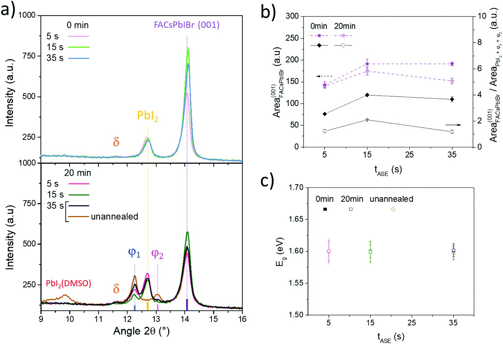
To better understand the effect of the processing conditions on cell performance, the perovskite layer has been further characterized. As mentioned previously, all the tested tASE promote the nucleation and growth of the same few crystal phases (FACsPbIBr, PbI2 and δ-FAPbI3), Fig. 8a (top graph) and Fig. S9 (ESI†). From a quantitative standpoint, the ratio of perovskite phases relative to PbI2 was evaluated with the surface of the corresponding diffraction peaks, Fig. 8b. The maximum is reached for a tASE close to 15 s. At this value, the width at the mid-height of the diffraction peak at 14.1° according to orientation (001) is also minimal. For the other orientations, the largest variations are observed for the (111) orientation, Fig. S10 (ESI†). The ratio of orientations (111) and (001) is minimal for a tASE of 15 s, confirming the strong (001) orientation at this stage of tASE. This could partially explain the evolution of the Voc with tASE.36
 | ||
| Fig. 8 (a) Zoom of X-ray diffraction patterns of perovskite layers for 2θ between 10° and 16° for different conditions of tASE (for tDBA = 0 min on top and tDBA = 20 min at the bottom); (b) areas of the main diffraction peaks relating to the FACsPbIBr phase and of the ratio of the FACsPbIBr phases compared to PbI2, φ1 and φ2 phases as a function of the tASE for tDBA of 0 and 20 min; and (c) optical bandgap of the perovskite layers for the different tested conditions (calculated using the Tauc plot method). | ||
Concerning the combined influence of tASE and tDBA, in addition to the same phases already observed, two new crystal phases φ1 and φ2 are detected when tDBA is applied, Fig. 8a (bottom graph). Their diffraction peaks appear respectively at 12.2–12.3° and 13.1°. According to the literature, these phases seem to correspond to the phases denoted 6H and 4H of the study by Gratia et al.,78 which concerns the intermediate phases possibly observed in mixed perovskites during its conversion process.78 The latter is crystalline intermediates between the δ-FAPbI3 and perovskite phases. The peak at 13.1°, i.e. the φ2 phase, can also correspond to the PbX2 phase, located between 13.1° and 13.2°.22 However, the absorbance spectra obtained on the same samples show optical transitions similar to the intermediate phases reported by Gratia et al.78 This therefore seems to confirm the hypothesis of the formation of crystalline intermediates induced by the application of tDBA. However, very little work concerns the study of these two phases, in particular their optoelectronic properties and therefore their impact on the PV performance of cells produced from these perovskites.
Here, when tDBA is applied, φ1 and φ2 phases are formed during the drying step, together with the improvement in the perovskite layer's morphology. Both may thus have a role to play in the assessed enhancements in PV performances and/or be interconnected. Regarding the final thermal annealing step, it allows the elimination of the remaining PbI2(DMSO) complexes undoubtedly79 responsible for the limited FF and Jsc values previously described for devices elaborated with the condition of 35 s/unannealed.
Furthermore, it is important to note that the angular positions of all diffraction peaks relative to the perovskite remain unchanged after application of tDBA, indicating conservation of crystal lattice parameters. This is supported by UV-Visible spectroscopy analyses, which after exploitation of the Tauc plots show a constancy of the bandgap whatever the tASE and tDBA conditions, Fig. 8c. In parallel, as shown in Fig. 8b (dotted lines), there is a loss of the FACsPbIBr phase in favor of the formation of other crystalline phases (PbI2, φ1 and φ2). This trend seems to be confirmed for each tASE, Fig. 8b. This also seems to correspond to a loss of absorption as shown in Fig. S11 (ESI†). As shown in Fig. S10 (ESI†), the FACsPbIBr phase is further disoriented as tASE increases for a tDBA of 20 min. At the same time, widening of the width at half the height of the main diffraction peak of this phase is also noted, indicating a reduction of the crystal quality. Given the changes in efficiencies granted by the FF and Voc improvements with tDBA, these changes appear to be of lesser importance or at least the formation of these new phases (φ1 and φ2) seems to compensate for the decreased proportion of the perovskite phase and its lower quality.
Regarding the photoluminescence spectroscopy results, shown in Fig. 9a, if tASE seems to have no effect on the peak position, a blue-shift can be typically observed when tDBA is applied. Due to the constancy of the optical bandgap observed previously, it can therefore be said that this cannot be explained by a chemical modification of the perovskite but by a probable improvement in the properties of the electronic defects within the perovskite layer. Indeed, the energy states of the electronic traps can be located in shallower states within the bandgap and this, coupled with a lower defect density, can lead to a spectral blue-shift in the PL position.80 This could explain the performance gains observed only for 15 s and 35 s tASE. In addition, the results of the measurements carried out using a Kelvin probe are presented in Fig. 9b. In fact, the addition of tDBA seems to systematically decrease the work function (Fermi level) of the perovskite layer by about 0.1 eV for the three tASE tested. It is therefore conceivable that the energy positions of valence and conduction bands are also modified. These changes in energetic properties are likely the overall result of all the previously described modifications brought by the room temperature additional drying step.
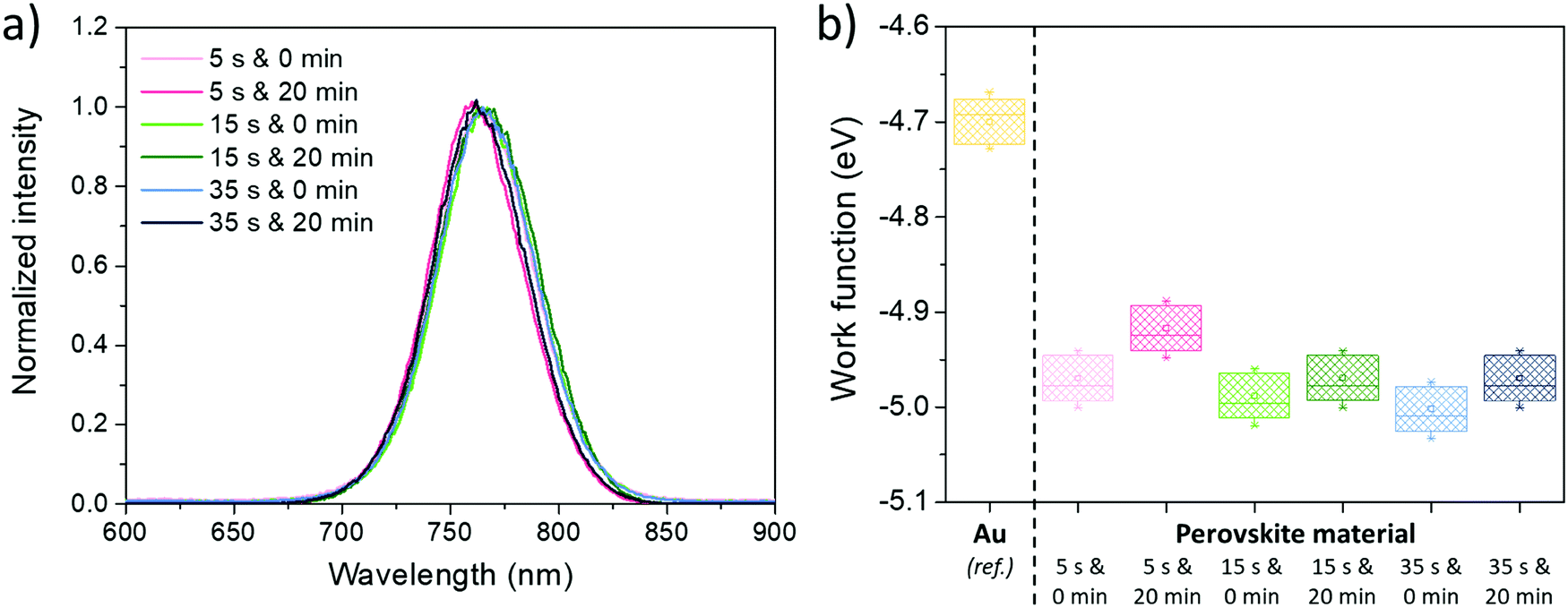 | ||
| Fig. 9 (a) PL spectra for the different tested tASE and tDBA, and (b) work functions of perovskite layers developed according to different conditions of tASE and tDBA. | ||
To check the stability of these phases, an ageing study has been performed (in a glovebox, and under dark and room temperature conditions), Fig. S12 (ESI†). Overall, the PV parameters are stable for at least 450 h. We however note a slight decrease of these parameters, probably because of the insufficient barrier level of the N-type layer regarding the diffusion of the silver electrode and perovskite compounds.81 This can be overcome by adding an ITO layer between SnO2 and Ag layers, which can act as a barrier against diffusion, Fig. S12 (ESI†). Therefore, the perovskite layer and its crystalline phases are intrinsically stable over time. Finally, the hysteresis phenomenon of these solar cells has been evaluated before and after aging, Fig. S13 (ESI†). It is relatively stable over time and the hysteresis index82 was found to be close to 10%. Thus, the optimization performed seems to be sustainable over time and generates a low hysteresis phenomenon.
Conclusions
In this paper, the development of innovative perovskite cells with PIN architecture has been achieved through a material/process optimization approach. Thanks to a previous study carried out in the NIP architecture, the formulation of the perovskite used as an active layer was optimized. Then, the first optimization phase developed in this article concerned the perovskite deposition process according to the HTL beneath, thanks to the change of anti-solvent and the optimization of the anti-solvent ejection time. The interest in the PTAA and TFB layers was immediately highlighted, characterized by their potential for higher Voc. The study was then refocused on TFB as the HTL due to its more suitable intrinsic properties and lower explored investigations in PV literature. After an optimization of the concentration of the perovskite solution, the double optimization of the anti-solvent ejection time (tASE) and the drying time before annealing (tDBA) was performed, allowing improvement in the PCE of our devices from 10% to 17% with an optimized Voc of about 1.1V. One of the important results of this study is the methodology used for this optimization. Indeed, the main marker used is the observation of defects in the perovskite layer at the macroscopic and microscopic scales. This optimization of the perovskite layer morphology leads to a significant increase in performance. The additional gain in performance is then obtained by optimizing the nanostructure and in particular by defining markers resulting mainly from XRD analyses such as perovskite/PbI2 phase ratios. The formation of the φ1 and φ2 phases seems to have a very positive effect on the nanostructure of the perovskite and thus on its optoelectronic properties.Abbreviations
| t DBA | Drying time before annealing |
| t ASE | Anti-solvent ejection time |
| ETL | Electron transport layer (n) |
| FA | FormAmidinium |
| FF | Fill factor |
| GMF | Glass microFiber |
| HTL | Hole transport layer (p) |
| IPA | IsoPropyl alcohol |
| ITO | Indium tin oxide |
| J–V | Current density–voltage |
| J sc | Short-circuit current density |
| MA | MethylAmmonium |
| MAPI | MAPbI3 |
| PCE | Power conversion efficiency |
| PEDOT:PSS | Poly(3,4-ethyleneDiOxyThiophene): poly(styrenesulfonate) |
| PL | PhotoLuminescence |
| PSC | Perovskite solar cell |
| PTAA | Poly(triaryl amine) |
| PTFE | Polytetrafluoroethylene |
| PV | Photovoltaic |
| Roc | Resistance at open circuit condition |
| R s | Series resistance |
| R sc | Resistance at short circuit condition |
| SEM | Scanning electron microscope |
| TFB | Poly[(9,9-dioctylfluorenyl-2,7-diyl)-co-(4,4′-(N-(p-butylphenyl))diphenylamine)] |
| V oc | Open-circuit voltage |
| XRD | X-Ray diffraction |
| NIP | Negative-intrinsic-positive solar cell architecture |
| PIN | Positive-intrinsic-negative solar cell architecture |
| spiro-OMeTAD | 2,2′,7,7′-Tetrakis[N,N-di(4-methoxyphenyl)amino]-9,9′-spirobifluorene |
Conflicts of interest
There are no conflicts to declare.Acknowledgements
This work was financed by the Conseil Savoie Mont Blanc, University Savoie Mont Blanc, and Commissariat à l’énergie atomique et aux énergies alternatives. This work has been supported by the French National Research Agency, through Investments for Future Program (ref. ANR-18-EURE-0016 -Solar Academy). The research unit LEPMI is a member of the INES Solar Academy Research Center.References
- NREL. Best Research-Cell Efficiencies: Rev. 04-06-2020. Best Research-Cell Efficiency Chart | Photovoltaic Research | NREL. 2020.
- H. J. Snaith, Present status and future prospects of perovskite photovoltaics, Nat. Mater., 2018, 17, 372–376, DOI:10.1038/s41563-018-0071-z.
- G. E. Eperon, S. D. Stranks, C. Menelaou, M. B. Johnston, L. M. Herz and H. J. Snaith, Formamidinium Lead Trihalide: A Broadly Tunable Perovskite for Efficient Planar Heterojunction Solar Cells, Energy Environ. Sci., 2014, 7, 982–988, 10.1039/C3EE43822H.
- L. M. Herz, Charge-Carrier Mobilities in Metal Halide Perovskites: Fundamental Mechanisms and Limits, ACS Energy Lett., 2017, 2(7), 1539–1548, DOI:10.1021/acsenergylett.7b00276.
- S. De Wolf, J. Holovsky, S. J. Moon, P. Löper, B. Niesen, M. Ledinsky, F. J. Haug, J. H. Yum and C. Ballif, Organometallic Halide Perovskites: Sharp Optical Absorption Edge and Its Relation to Photovoltaic Performance, J. Phys. Chem. Lett., 2014, 5(6), 1035–1039, DOI:10.1021/jz500279b.
- Q. Wali, N. K. Elumalai, Y. Iqbal, A. Uddin and R. Jose, Tandem Perovskite Solar Cells, Renewable Sustainable Energy Rev., 2018, 84, 89–110, DOI:10.1016/j.rser.2018.01.005.
- M. Jošt, L. Kegelmann, L. Korte and S. Albrecht, Monolithic Perovskite Tandem Solar Cells: A Review of the Present Status and Advanced Characterization Methods Toward 30% Efficiency, Adv. Energy Mater., 2020, 10, 1904102, DOI:10.1002/aenm.201904102.
- S. Rühle, Tabulated Values of the Shockley-Queisser Limit for Single Junction Solar Cells, Sol. Energy, 2016, 130, 139–147, DOI:10.1016/j.solener.2016.02.015.
- A. Kojima, K. Teshima, Y. Shirai and T. Miyasaka, Organometal Halide Perovskites as Visible-Light Sensitizers for Photovoltaic Cells, J. Am. Chem. Soc., 2009, 131(17), 6050–6051, DOI:10.1021/ja809598r.
- J. Y. Jeng, Y. F. Chiang, M. H. Lee, S. R. Peng, T. F. Guo, P. Chen and T. C. Wen, CH3NH3PbI3 Perovskite/Fullerene Planar-Heterojunction Hybrid Solar Cells, Adv. Mater., 2013, 25(27), 3727–3732, DOI:10.1002/adma.201301327.
- W. S. Yang, B. W. Park, E. H. Jung, N. J. Jeon, Y. C. Kim, D. U. Lee, S. S. Shin, J. Seo, E. K. Kim and J. H. Noh, et al., Iodide Management in Formamidinium-Lead-Halide-Based Perovskite Layers for Efficient Solar Cells, Science (80-.), 2017, 356(6345), 1376–1379, DOI:10.1126/science.aan2301.
- A. Al-Ashouri, A. Magomedov, M. Roß, M. Jošt, M. Talaikis, G. Chistiakova, T. Bertram, J. A. Márquez, E. Köhnen and E. Kasparavičius, et al., Conformal Monolayer Contacts with Lossless Interfaces for Perovskite Single Junction and Monolithic Tandem Solar Cells, Energy Environ. Sci., 2019, 12, 3356–3369, 10.1039/c9ee02268f.
- B. Conings, A. Babayigit, M. T. Klug, S. Bai, N. Gauquelin, N. Sakai, J. T. W. Wang, J. Verbeeck, H. G. Boyen and H. J. Snaith, A Universal Deposition Protocol for Planar Heterojunction Solar Cells with High Efficiency Based on Hybrid Lead Halide Perovskite Families, Adv. Mater., 2016, 28(48), 10701–10709, DOI:10.1002/adma.201603747.
- H. Shen, D. Walter, Y. Wu, K. C. Fong, D. A. Jacobs, T. Duong, J. Peng, K. Weber, T. P. White and K. R. Catchpole, Monolithic Perovskite/Si Tandem Solar Cells: Pathways to Over 30% Efficiency, Adv. Energy Mater., 2020, 10(13), 1902824, DOI:10.1002/aenm.201902840.
- M. Jošt, E. Köhnen, A. B. Morales-Vilches, B. Lipovšek, K. Jäger, B. Macco, A. Al-Ashouri, J. Krč, L. Korte and B. Rech, et al., Textured Interfaces in Monolithic Perovskite/Silicon Tandem Solar Cells: Advanced Light Management for Improved Efficiency and Energy Yield, Energy Environ. Sci., 2018, 11, 3511–3523, 10.1039/c8ee02469c.
- K. A. Bush, S. Manzoor, K. Frohna, Z. J. Yu, J. A. Raiford, A. F. Palmstrom, H. P. Wang, R. Prasanna, S. F. Bent and Z. C. Holman, et al., Minimizing Current and Voltage Losses to Reach 25% Efficient Monolithic Two-Terminal Perovskite-Silicon Tandem Solar Cells, ACS Energy Lett., 2018, 3(9), 2173–2180, DOI:10.1021/acsenergylett.8b01201.
- F. Sahli, J. Werner, B. A. Kamino, M. Bräuninger, R. Monnard, B. Paviet-Salomon, L. Barraud, L. Ding, J. J. Diaz Leon and D. Sacchetto, et al., Fully Textured Monolithic Perovskite/Silicon Tandem Solar Cells with 25.2% Power Conversion Efficiency, Nat. Mater., 2018, 17, 820–826, DOI:10.1038/s41563-018-0115-4.
- C. O. Ramírez Quiroz, Y. Shen, M. Salvador, K. Forberich, N. Schrenker, G. D. Spyropoulos, T. Heumüller, B. Wilkinson, T. Kirchartz and E. Spiecker, et al., Balancing Electrical and Optical Losses for Efficient 4-Terminal Si-Perovskite Solar Cells with Solution Processed Percolation Electrodes, J. Mater. Chem. A, 2018, 6, 3583–3592, 10.1039/c7ta10945h.
- F. Fu, T. Feurer, T. P. Weiss, S. Pisoni, E. Avancini, C. Andres, S. Buecheler and A. N. Tiwari, High-Efficiency Inverted Semi-Transparent Planar Perovskite Solar Cells in Substrate Configuration, Nat. Energy, 2017, 2, 16190, DOI:10.1038/nenergy.2016.190.
- Z. Wei, B. Smith, F. De Rossi, J. R. Searle, D. A. Worsley and T. M. Watson, Efficient and Semi-Transparent Perovskite Solar Cells Using a Room-Temperature Processed MoO: X/ITO/Ag/ITO Electrode, J. Mater. Chem. C, 2019, 7, 10981–10987, 10.1039/c9tc03684a.
- J. Xu, C. C. Boyd, Z. J. Yu, A. F. Palmstrom, D. J. Witter, B. W. Larson, R. M. France, J. Werner, S. P. Harvey and E. J. Wolf, et al., Triple-Halide Wide-Band Gap Perovskites with Suppressed Phase Segregation for Efficient Tandems, Science, 2020, 367, 6482, DOI:10.1126/science.aaz4639.
- D. Luo, W. Yang, Z. Wang, A. Sadhanala, Q. Hu, R. Su, R. Shivanna, G. F. Trindade, J. F. Watts and Z. Xu, et al., Enhanced Photovoltage for Inverted Planar Heterojunction Perovskite Solar Cells, Science, 2018, 360, 6396, DOI:10.1126/science.aap9282.
- M. Saliba, T. Matsui, J. Y. Seo, K. Domanski, J. P. Correa-Baena, M. K. Nazeeruddin, S. M. Zakeeruddin, W. Tress, A. Abate and A. Hagfeldt, et al., Cesium-Containing Triple Cation Perovskite Solar Cells: Improved Stability, Reproducibility and High Efficiency, Energy Environ. Sci., 2016, 9, 1989–1997, 10.1039/c5ee03874j.
- S. Shukla, S. Shukla, L. J. Haur, S. S. H. Dintakurti, G. Han, A. Priyadarshi, T. Baikie, S. G. Mhaisalkar and N. Mathews, Effect of Formamidinium/Cesium Substitution and PbI2 on the Long-Term Stability of Triple-Cation Perovskites, ChemSusChem, 2017, 10(19), 3804–3809, DOI:10.1002/cssc.201701203.
- K. Jäger, L. Korte, B. Rech and S. Albrecht, Numerical Optical Optimization of Monolithic Planar Perovskite-Silicon Tandem Solar Cells with Regular and Inverted Device Architectures, Opt. Express, 2017, 25, A473–A482, DOI:10.1364/oe.25.00a473.
- E. Planes, L. Perrin, M. Matheron, M. Spalla, S. Berson and L. Flandin, Degradation Mechanisms in a Mixed Cations and Anions Perovskite Solar Cell: Mitigation Effect of the Gold Electrode, ACS Appl. Energy Mater., 2021, 4(2), 1365–1376, DOI:10.1021/acsaem.0c02613.
- D. Yang, T. Sano, Y. Yaguchi, H. Sun, H. Sasabe and J. Kido, Achieving 20% Efficiency for Low-Temperature-Processed Inverted Perovskite Solar Cells, Adv. Funct. Mater., 2019, 29(12), 1807556, DOI:10.1002/adfm.201807556.
- H. Kwon, J. W. Lim, J. Han, L. N. Quan, D. Kim, E. S. Shin, E. Kim, D. W. Kim, Y. Y. Noh and I. Chung, et al., Towards Efficient and Stable Perovskite Solar Cells Employing Non-Hygroscopic F4-TCNQ Doped TFB as the Hole-Transporting Material, Nanoscale, 2019, 11, 19586–19594, 10.1039/c9nr05719f.
- M. H. Li, S. C. Liu, F. Z. Qiu, Z. Y. Zhang, D. J. Xue and J. S. Hu, High-Efficiency CsPbI2Br Perovskite Solar Cells with Dopant-Free Poly(3-Hexylthiophene) Hole Transporting Layers, Adv. Energy Mater., 2020, 10(21), 2000501, DOI:10.1002/aenm.202000501.
- X. Xu, C. Ma, Y. Cheng, Y. M. Xie, X. Yi, B. Gautam, S. Chen, H. W. Li, C. S. Lee and F. So, et al., Ultraviolet-Ozone Surface Modification for Non-Wetting Hole Transport Materials Based Inverted Planar Perovskite Solar Cells with Efficiency Exceeding 18%, J. Power Sources, 2017, 360, 157–165, DOI:10.1016/j.jpowsour.2017.06.013.
- X. Liu, Y. Cheng, C. Liu, T. Zhang, N. Zhang, S. Zhang, J. Chen, Q. Xu, J. Ouyang and H. Gong, 20.7% Highly Reproducible Inverted Planar Perovskite Solar Cells with Enhanced Fill Factor and Eliminated Hysteresis, Energy Environ. Sci., 2019, 12, 1622, 10.1039/c9ee90024a.
- A. Kahn, Fermi Level, Work Function and Vacuum Level, Mater. Horiz., 2016, 3, 7–10, 10.1039/c5mh00160a.
- Z. Li, M. Yang, J. S. Park, S. H. Wei, J. J. Berry and K. Zhu, Stabilizing Perovskite Structures by Tuning Tolerance Factor: Formation of Formamidinium and Cesium Lead Iodide Solid-State Alloys, Chem. Mater., 2016, 28(1), 284–292, DOI:10.1021/acs.chemmater.5b04107.
- W. Tan, A. R. Bowring, A. C. Meng, M. D. McGehee and P. C. McIntyre, Thermal Stability of Mixed Cation Metal Halide Perovskites in Air, ACS Appl. Mater. Interfaces, 2018, 28(1), 284–292, DOI:10.1021/acsami.7b15263.
- Y. Bai, X. Meng and S. Yang, Interface Engineering for Highly Efficient and Stable Planar P-i-n Perovskite Solar Cells, Adv. Energy Mater., 2018, 8(5), 1701883, DOI:10.1002/aenm.201701883.
- X. Zheng, Y. Hou, C. Bao, J. Yin, F. Yuan, Z. Huang, K. Song, J. Liu, J. Troughton and N. Gasparini, et al., Managing Grains and Interfaces via Ligand Anchoring Enables 22.3%-Efficiency Inverted Perovskite Solar Cells, Nat. Energy, 2020, 5, 131–140, DOI:10.1038/s41560-019-0538-4.
- K. A. Bush, C. D. Bailie, Y. Chen, A. R. Bowring, W. Wang, W. Ma, T. Leijtens, F. Moghadam and M. D. McGehee, Thermal and Environmental Stability of Semi-Transparent Perovskite Solar Cells for Tandems Enabled by a Solution-Processed Nanoparticle Buffer Layer and Sputtered ITO Electrode, Adv. Mater., 2016, 28(20), 3937–3943, DOI:10.1002/adma.201505279.
- J. Pascual, J. L. Delgado and R. Tena-Zaera, Physicochemical Phenomena and Application in Solar Cells of Perovskite:Fullerene Films, J. Phys. Chem. Lett., 2018, 9(11), 2893–2902, DOI:10.1021/acs.jpclett.8b00968.
- P. W. Liang, C. C. Chueh, S. T. Williams and A. K. Y. Jen, Roles of Fullerene-Based Interlayers in Enhancing the Performance of Organometal Perovskite Thin-Film Solar Cells, Adv. Energy Mater., 2015, 5(10), 1402321, DOI:10.1002/aenm.201402321.
- Y. Chen, Q. Meng, L. Zhang, C. Han, H. Gao, Y. Zhang and H. Yan, SnO2-Based Electron Transporting Layer Materials for Perovskite Solar Cells: A Review of Recent Progress, J. Energy Chem., 2019, 35, 144–167, DOI:10.1016/j.jechem.2018.11.011.
- C. Bi, Q. Wang, Y. Shao, Y. Yuan, Z. Xiao and J. Huang, Non-Wetting Surface-Driven High-Aspect-Ratio Crystalline Grain Growth for Efficient Hybrid Perovskite Solar Cells, Nat. Commun., 2015, 6, 7747, DOI:10.1038/ncomms8747.
- Y. Xia and S. Dai, Review on Applications of PEDOTs and PEDOT:PSS in Perovskite Solar Cells, J. Mater. Sci.: Mater. Electron., 2021, 32, 12746–12757, DOI:10.1007/s10854-020-03473-w.
- M. Stolterfoht, P. Caprioglio, C. M. Wolff, J. A. Márquez, J. Nordmann, S. Zhang, D. Rothhardt, U. Hörmann, Y. Amir and A. Redinger, et al., The Impact of Energy Alignment and Interfacial Recombination on the Internal and External Open-Circuit Voltage of Perovskite Solar Cells, Energy Environ. Sci., 2019, 12, 2778–2788, 10.1039/c9ee02020a.
- H. H. Fong, A. Papadimitratos, J. Hwang, A. Kahn and G. G. Malliaras, Hole Injection in a Model Fluorene-Triarylamine Copolymer, Adv. Funct. Mater., 2009, 19, 304–310, DOI:10.1002/adfm.200800738.
- S. Ghosh, S. Mishra and T. Singh, Antisolvents in Perovskite Solar Cells: Importance, Issues, and Alternatives, Adv. Mater. Interfaces, 2020, 7(18), 2000950, DOI:10.1002/admi.202000950.
- A. D. Taylor, Q. Sun, K. P. Goetz, Q. An, T. Schramm, Y. Hofstetter, M. Litterst, F. Paulus and Y. Vaynzof, A General Approach to High-Efficiency Perovskite Solar Cells by Any Antisolvent, Nat. Commun., 2021, 12, 1878, DOI:10.1038/s41467-021-22049-8.
- F. H. Isikgor, A. S. Subbiah, M. K. Eswaran, C. T. Howells, A. Babayigit, M. De Bastiani, E. Yengel, J. Liu, F. Furlan and G. T. Harrison, et al., Scaling-up Perovskite Solar Cells on Hydrophobic Surfaces, Nano Energy, 2021, 81, 105633, DOI:10.1016/j.nanoen.2020.105633.
- M. Stolterfoht, C. M. Wolff, J. A. Márquez, S. Zhang, C. J. Hages, D. Rothhardt, S. Albrecht, P. L. Burn, P. Meredith and T. Unold, et al., Visualization and Suppression of Interfacial Recombination for High-Efficiency Large-Area Pin Perovskite Solar Cells, Nat. Energy, 2018, 3, 847–854, DOI:10.1038/s41560-018-0219-8.
- S. Li, F. Zhang, Q. Sun, Z. Li, Y. Cui, T. Ji, W. Qin, F. Zhu and Y. Hao, Entire Mirror-like Perovskite Films for High-Performance Perovskite Solar Cells: The Role of Polar Anti-Solvent Sec-Pentyl Alcohol, Org. Electron., 2018, 57, 133–139, DOI:10.1016/j.orgel.2018.03.003.
- J. Troughton, K. Hooper and T. M. Watson, Humidity Resistant Fabrication of CH3NH3PbI3 Perovskite Solar Cells and Modules, Nano Energy, 2017, 39, 60–68, DOI:10.1016/j.nanoen.2017.06.039.
- Z. Wei and J. Xing, The Rise of Perovskite Light-Emitting Diodes, J. Phys. Chem. Lett., 2019, 10(11), 3035–3042, DOI:10.1021/acs.jpclett.9b00277.
- M. P. Montoya, S. Sidhik, D. Esparza, T. López-Luke, I. Zarazua, J. M. Rivas and E. De la Rosa, Study of Inverted Planar CH3NH3PbI3 Perovskite Solar Cells Fabricated under Environmental Conditions, Sol. Energy, 2019, 180, 594–600, DOI:10.1016/j.solener.2019.01.061.
- Y. Rong, Z. Tang, Y. Zhao, X. Zhong, S. Venkatesan, H. Graham, M. Patton, Y. Jing, A. M. Guloy and Y. Yao, Solvent Engineering towards Controlled Grain Growth in Perovskite Planar Heterojunction Solar Cells, Nanoscale, 2015, 7, 10595–10599, 10.1039/c5nr02866c.
- S. Park, H. Lee, H. Lee, D. Shin and Y. Yi, Impact of Diethyl Ether Dripping Delay Time on the Electronic Structure of Methylammonium Lead Triiodide Perovskite Film, J. Korean Phys. Soc., 2020, 76, 162–166, DOI:10.3938/jkps.76.162.
- P. Terpstra and H. G. Westenbrink, On the Crystal-Structure of Lead-Iodide, Proc. K. Ned. Akad. Wet., 1926, 29, 431 Search PubMed.
- A. A. Zhumekenov, M. I. Saidaminov, M. A. Haque, E. Alarousu, S. P. Sarmah, B. Murali, I. Dursun, X. H. Miao, A. L. Abdelhady and T. Wu, et al., Formamidinium Lead Halide Perovskite Crystals with Unprecedented Long Carrier Dynamics and Diffusion Length, ACS Energy Lett., 2016, 1(1), 32–37, DOI:10.1021/acsenergylett.6b00002.
- Q. Chen, H. Zhou, Y. Fang, A. Z. Stieg, T. Song, Bin, H. H. Wang, X. Xu, Y. Liu, S. Lu and J. You, et al., The Optoelectronic Role of Chlorine in CH3NH3PbI3 (Cl)-Based Perovskite Solar Cells, Nat. Commun., 2015, 6, 7269, DOI:10.1038/ncomms8269.
- F. Bella, P. Renzi, C. Cavallo and C. Gerbaldi, Caesium for Perovskite Solar Cells: An Overview, Chemistry - A European Journal, 2018, 24(47), 12183–12205, DOI:10.1002/chem.201801096.
- H. Kim, K. G. Lim and T. W. Lee, Planar Heterojunction Organometal Halide Perovskite Solar Cells: Roles of Interfacial Layers, Energy Environ. Sci., 2016, 9, 12–30, 10.1039/c5ee02194d.
- Q. Dong, Y. Yuan, Y. Shao, Y. Fang, Q. Wang and J. Huang, Abnormal Crystal Growth in CH3NH3PbI3−XClx Using a Multi-Cycle Solution Coating Process, Energy Environ. Sci., 2015, 8, 2464–2470, 10.1039/c5ee01179e.
- L. Meng, C. Sun, R. Wang, W. Huang, Z. Zhao, P. Sun, T. Huang, J. Xue, J. W. Lee and C. Zhu, et al., Tailored Phase Conversion under Conjugated Polymer Enables Thermally Stable Perovskite Solar Cells with Efficiency Exceeding 21%, J. Am. Chem. Soc., 2018, 140(49), 17255–17262, DOI:10.1021/jacs.8b10520.
- F. Zhang, J. Song, R. Hu, Y. Xiang, J. He, Y. Hao, J. Lian, B. Zhang, P. Zeng and J. Qu, Interfacial Passivation of the P-Doped Hole-Transporting Layer Using General Insulating Polymers for High-Performance Inverted Perovskite Solar Cells, Small, 2018, 14(19), 1704007, DOI:10.1002/smll.201704007.
- S. K. Jung, J. H. Heo, D. W. Lee, S. C. Lee, S. H. Lee, W. Yoon, H. Yun, S. H. Im, J. H. Kim and O. P. Kwon, Nonfullerene Electron Transporting Material Based on Naphthalene Diimide Small Molecule for Highly Stable Perovskite Solar Cells with Efficiency Exceeding 20%, Adv. Funct. Mater., 2018, 28(20), 1800346, DOI:10.1002/adfm.201800346.
- Y. J. Pu, T. Chiba, K. Ideta, S. Takahashi, N. Aizawa, T. Hikichi and J. Kido, Fabrication of Organic Light-Emitting Devices Comprising Stacked Light-Emitting Units by Solution-Based Processes, Adv. Mater., 2015, 27, 1327–1332, DOI:10.1002/adma.201403973.
- Q. Xu, W. Shao, X. Zhang, J. Liu, X. Ouyang, X. Tang and W. Jia, Low-Temperature Photoluminescence Spectroscopy of CH3NH3PbBrxCl3−x Perovskite Single Crystals, J. Alloys Compd., 2019, 792, 185–190, DOI:10.1016/j.jallcom.2019.04.016.
- Z. Liu, A. Zhu, F. Cai, L. M. Tao, Y. Zhou, Z. Zhao, Q. Chen, Y. B. Cheng and H. Zhou, Nickel Oxide Nanoparticles for Efficient Hole Transport in P–i–n and n–i–p Perovskite Solar Cells, J. Mater. Chem. A, 2017, 5, 6597–6605, 10.1039/c7ta01593c.
- M. Yin, F. Xie, H. Chen, X. Yang, F. Ye, E. Bi, Y. Wu, M. Cai and L. Han, Annealing-Free Perovskite Films by Instant Crystallization for Efficient Solar Cells, J. Mater. Chem. A, 2016, 5, 842–847, 10.1039/c6ta02490d.
- H. Yu, X. Liu, Y. Xia, Q. Dong, K. Zhang, Z. Wang, Y. Zhou, B. Song and Y. Li, Room-Temperature Mixed-Solvent-Vapor Annealing for High Performance Perovskite Solar Cells, J. Mater. Chem. A, 2015, 4, 321–326, 10.1039/c5ta08565a.
- J. W. Lee, D. H. Kim, H. S. Kim, S. W. Seo, S. M. Cho and N. G. Park, Formamidinium and Cesium Hybridization for Photo- and Moisture-Stable Perovskite Solar Cell, Adv. Energy Mater., 2015, 5(20), 1501310, DOI:10.1002/aenm.201501310.
- Y. Zhou, M. Yang, W. Wu, A. L. Vasiliev, K. Zhu and N. P. Padture, Room-Temperature Crystallization of Hybrid-Perovskite Thin Films via Solvent-Solvent Extraction for High-Performance Solar Cells, J. Mater. Chem. A, 2015, 3, 8178–8184, 10.1039/c5ta00477b.
- L. Huang, Z. Hu, J. Xu, K. Zhang, J. Zhang and Y. Zhu, Multi-Step Slow Annealing Perovskite Films for High Performance Planar Perovskite Solar Cells, Sol. Energy Mater. Sol. Cells, 2015, 141, 377–382, DOI:10.1016/j.solmat.2015.06.018.
- T. Matsui, J. Y. Seo, M. Saliba, S. M. Zakeeruddin and M. Grätzel, Room-Temperature Formation of Highly Crystalline Multication Perovskites for Efficient, Low-Cost Solar Cells, Adv. Mater., 2017, 29(15), 1606258, DOI:10.1002/adma.201606258.
- H. S. Duan, H. Zhou, Q. Chen, P. Sun, S. Luo, T. Song, Bin, B. Bob and Y. Yang, The Identification and Characterization of Defect States in Hybrid Organic-Inorganic Perovskite Photovoltaics, Phys. Chem. Chem. Phys., 2015, 17, 112–116, 10.1039/c4cp04479g.
- A. Dualeh, N. Tétreault, T. Moehl, P. Gao, M. K. Nazeeruddin and M. Grätzel, Effect of Annealing Temperature on Film Morphology of Organic-Inorganic Hybrid Pervoskite Solid-State Solar Cells, Adv. Funct. Mater., 2014, 24(21), 3250–3258, DOI:10.1002/adfm.201304022.
- Y. Deng, X. Zheng, Y. Bai, Q. Wang, J. Zhao and J. Huang, Surfactant-Controlled Ink Drying Enables High-Speed Deposition of Perovskite Films for Efficient Photovoltaic Modules, Nat. Energy, 2018, 3, 560–566, DOI:10.1038/s41560-018-0153-9.
- T. S. Sherkar, C. Momblona, L. Gil-Escrig, J. Ávila, M. Sessolo, H. J. Bolink and L. J. A. Koster, Recombination in Perovskite Solar Cells: Significance of Grain Boundaries, Interface Traps, and Defect Ions, ACS Energy Lett., 2017, 2(5), 1214–1222, DOI:10.1021/acsenergylett.7b00236.
- M. V. Kovalenko, L. Protesescu and M. I. Bodnarchuk, Properties and Potential Optoelectronic Applications of Lead Halide Perovskite Nanocrystals, Science, 2017, 358, 745–750, DOI:10.1126/science.aam7093.
- P. Gratia, I. Zimmermann, P. Schouwink, J. H. Yum, J. N. Audinot, K. Sivula, T. Wirtz and M. K. Nazeeruddin, The Many Faces of Mixed Ion Perovskites: Unraveling and Understanding the Crystallization Process, ACS Energy Lett., 2017, 2(12), 2686–2693, DOI:10.1021/acsenergylett.7b00981.
- W. S. Yang, J. H. Noh, N. J. Jeon, Y. C. Kim, S. Ryu, J. Seo and S. I. l. Seok, High-Performance Photovoltaic Perovskite Layers Fabricated through Intramolecular Exchange, Science, 2015, 348(6240), 1234–1237, DOI:10.1126/science.aaa9272.
- H. H. Fang, S. Adjokatse, S. Shao, J. Even and M. A. Loi, Long-Lived Hot-Carrier Light Emission and Large Blue Shift in Formamidinium Tin Triiodide Perovskites, Nat. Commun., 2018, 9, 243, DOI:10.1038/s41467-017-02684-w.
- C. C. Boyd, R. Cheacharoen, K. A. Bush, R. Prasanna, T. Leijtens and M. D. McGehee, Barrier Design to Prevent Metal-Induced Degradation and Improve Thermal Stability in Perovskite Solar Cells, ACS Energy Lett., 2018, 3(7), 1772–1778, DOI:10.1021/acsenergylett.8b00926.
- G. A. Nemnes, C. Besleaga, A. G. Tomulescu, A. Palici, L. Pintilie, A. Manolescu and I. Pintilie, How Measurement Protocols Influence the Dynamic J–V Characteristics of Perovskite Solar Cells: Theory and Experiment, Sol. Energy, 2018, 173, 976–983, DOI:10.1016/j.solener.2018.08.033.
Footnote |
| † Electronic supplementary information (ESI) available. See DOI: 10.1039/d1ma00819f |
| This journal is © The Royal Society of Chemistry 2021 |