DOI:
10.1039/D1MA00749A
(Paper)
Mater. Adv., 2021,
2, 7891-7906
Synergistic manifestation of band and scattering engineering in the single aliovalent Sb alloyed anharmonic SnTe alloy in concurrence with rule of parsimony†
Received
22nd August 2021
, Accepted 26th September 2021
First published on 29th September 2021
Abstract
Several endeavors were adapted to improve the thermoelectric performance of SnTe as a substitute of toxic PbTe and the booming approaches comprise introduction of nanostructuring, resonance states, valence band convergence and interstitial or substitutional defects. In this study, a stratagem was designed to incorporate single aliovalent Sb in SnTe by a one-step approach which successfully modulates the electronic and thermal transport properties by integration of several approaches, viz. energy-filtering effect, valence band convergence and phonon scattering at all length scales synergistically. Here, the alteration of the band structure of SnTe incorporated with Sb leads to substantial improvement of the Seebeck coefficient, essentially beneficial for the performance of thermoelectric alloys, beyond the designated critical temperature at 473 K which shows the onset of strong contribution of the heavy (Σ) valence band. The experimental finding of band convergence by Sb was for the first time corroborated by theoretical validation by Density Functional Theory (DFT) calculations. In addition, the presence of mass fluctuation, secondary precipitates, interfaces and the long-range interactions due to resonant bonding leading to optical phonon softening, large phase space available for three-phonon scattering and strong anharmonicity enables an ultralow lattice thermal conductivity of ∼0.5 W m−1 K−1. Thus, a zT value of ∼0.72 at 775 K is recorded for the SnTeSb0.05 composition, which is 154% enhancement compared to our pristine SnTe and is strongly competing with numerous reported zT values using considerably less abundant Ag, Ge, In and highly toxic Pb, Hg, Bi, Cd multiple elements as either a dopant or an additive. Thus, the law of parsimony is maintained with reduction in the cost of the thermoelectric module.
1. Introduction
Thermoelectric materials are employed for waste heat conversion into electricity or vice versa. The conversion efficiency depends on the dimensionless figure of merit (zT). For many decades, the scientific society worked for the enhancement of the figure of merit, but it rather depends on three interlinked parameters. The figure of merit can be defined as| |  | (1) |
where S, σ, κe, κl and T stand for the Seebeck coefficient, electrical conductivity, electronic thermal conductivity, lattice thermal conductivity and temperature, respectively.1 The interlacing of the terms demands optimization of zT judiciously. Hence, strategies need to be developed to search for alternative new materials with improved thermoelectric properties or towards the enhancement of zT of the state-of-the-art materials by optimizing the power factor (S2σ) via tuning the carrier concentration and by engineering the band structure.2 In the recent past, all-scale nano-mesostructuring3 and embedded endotaxial nanostructuring in the bulk matrix,4 complex crystal structures,2 soft phonon modes,5 lattice anharmonicity due to the presence of lone pairs,6,7 band nestification,8 anisotropic layered crystal structures,9,10 liquid-like cation disordering due to superionic substructures,11,12 band convergence,13–15 resonant bonding16 and resonant doping17–20 have been some of the ways which proved to be effective for reducing the intrinsic lattice thermal conductivity (κlat) or maximizing the power factor owing to its robustness against structural and temperature variation and grain size.
In the past couple of eras, Pb-chalcogenides, to be specific, PbTe, have been proven to be champion materials as far as thermoelectricity is concerned. They are highly robust for thermoelectric power generation for mid-temperature applications (400–600 K).21 However, their applications are constrained by reservations about Pb toxicity. Thus, in the search for Pb-free analogues, SnTe has appeared as an ecologically friendly alternative to PbTe for thermoelectric power generation because it exhibits a similar rock salt structure and electronic structure calculations have revealed a two-valence band structure analogous to PbTe.22 Nevertheless, in 1966, Dimmock et al. were the first to observe a small band gap of 0.18 eV for SnTe by photoluminescence experiments23 whereas in 1968 Rogers quantitatively resolved the large energy offset of ∼0.35 eV at 300 K,24 between the light valence band (L) and the heavy valence (Σ) band, which can be critical due to the remarkable bipolar diffusion and a poor Seebeck coefficient leading to a low power factor. He also pointed out that the light hole (L) valence band is forever highly nonparabolic and the heavy hole (Σ) valence band is parabolic. Moreover, the striking characteristic of SnTe unlike PbTe is that due to its characteristic off-stoichiometry (ultra-high hole density ∼1021 cm−3) associated with Sn vacancies, it shows highly degenerate transport properties and poor thermoelectric performances. Furthermore, the higher lattice thermal conductivity of SnTe in comparison to PbTe due to the low atomic mass of Sn compared to Pb leads to higher sound velocity at room temperature, which further lowers the zT.25,26
To improve the thermoelectric performance, the hole concentration must be reduced to the required level of 1019–1020 cm−3.27,28 Bhat et al. reported that Sn self-compensation up to 4 mol% would further increase the zT value to ∼0.7 in Sn1.04Te by further tuning the carrier concentration.29 Banik et al. reported that the presence of Sb by aliovalent cation doping enhances the electronic transport properties and thus optimizes the hole concentration in SnTe. An enhanced zT of ∼1 was obtained for the composition of Sn0.85Sb0.15Te at 800 K.30 Li et al. manipulated the interstitial defect in SnTe by Ge and Sb codoping. In this regard, Sn0.92Ge0.04Sb0.04Te–5% Cu2Te was found to exhibit an ultralow lattice thermal conductivity and a remarkably high zT of 1.5 at 873 K.31 Ma et al. integrated several optimization strategies using multi-nanostructure doping in a single thermoelectric SnTe material which optimized the properties and led to an ultralow κtot of ∼0.96 W m−1 K−1 and a high zT of ∼1.56 at 873 K in SnBi0.03Te–1% Mg3.2Sb0.6Bi1.4–0.2% MWCNTs due to the disturbance in electric potential at the interfaces between two dissimilar structures or elements and caused energy dependent scattering of carriers, leading to an energy filtering effect.30,32 Kihoi et al. reported that Mn and Bi codoping in SnTe leads to an overall zT of ∼0.93 at 773 K and a maximum conversion efficiency of ∼8.4% in the temperature range of 293–773 K.33 In addition, they also doped Sb to tune the carrier concentration leading to a zT of 1 at 773 K, with a lattice thermal conductivity of ∼0.86 W m−1 K−1 due to Mn rich nanoprecipitates.34 A record high power factor till date of ∼47 μW cm−1 K−2 was reported by Bhat et al. by co-doping Ca and In in SnTe leading to a zT of 1.65 at 840 K.35 However, the highest zT of 1.85 was reported by Hussain et al. by introduction of endotaxial nanostructuring leading to a slightly decreased power factor of ∼42.2 μW cm−1 K−2 and a lattice thermal conductivity of 0.75 W m−1 K−1.36
The intentional addition of Sb in SnTe is due to the fact that the aliovalent element, i.e. Sb, plays a vital role in optimization of lattice thermal conductivity in PbTe and SnTe based alloys by forming nanostructures via matrix encapsulation. Moreover, it is also reported that group IV–VI, V and V2–VI3 materials exhibit low thermal conductivity owing to their octahedral structure which results in weaker bonding due to the longer bond length,37 resonant bonding, long ranged interaction expected for resonant bonding38 and softening of transverse optical (TO) phonon mode leading to strong anharmonicity.39 Thus, the utmost material challenge for high thermoelectric performance is satisfied and employed to enhance the thermoelectric properties of SnTe using Sb additives. In addition, this paper is first of its kind to provide the theoretical validation of valence band convergence by Sb in SnTe by Density Functional Theory (DFT).
In this contribution, we report the realization of high thermoelectric performance of Sb-alloyed SnTe, instead of Sb-doped SnTe where the latter shows better performance when doped beyond the solubility limit of x ≥ 0.12. Herein, three separate synergistic approaches, viz., (a) suppression of excess hole concentration, (b) successful energy filtering and valence band convergence to increase the power factor, and (c) diminishing the lattice thermal conductivity, were considered to obtain an improved zT of ∼0.71 in SnTeSb0.05 at 773 K. Intension to avoid multiple metal doping circumvent the cost of thermoelectric modules. This simple and single step methodology is competitive with existing methodologies using considerably toxic and expensive elements, while maintaining the law of parsimony.
2. Methods
2.1. Experimental details
2.1.1. Starting materials.
Chemicals were used as received: Sn chunk (99.9999%, Sigma Aldrich), Te shot (99.999%, 5N, Sigma Aldrich), and Sb Chunk (99.999%, 5N, Alfa aesar).
2.1.2. Synthesis.
High-purity single elements Sn, Te, and Sb were weighed according to the stoichiometric composition of SnTeSbx (x = 0, 0.02, 0.03, 0.04, and 0.05) and then put inside 13 mm diameter fused quartz tubes. The tubes were sealed under vacuum (∼10−4 torr) and slowly heated to 900 °C at a rate of 50 °C per hour. The heated quartz tubes were then rocked at 900 °C continuously for 3 hours for homogenization and then soaked for 5 h. Subsequently, the quartz tubes were cooled slowly to room temperature at the rate of 70 °C per hour. The obtained ingots were then crushed and ground into powders inside a glove box (<1 ppm oxygen level) using a mortar and pestle for compaction. The ground powders were filled in a 12 mm diameter graphite die and sintered by spark plasma sintering (SPS, M/s. SPS Syntex, 725, Japan) at 773 K for SnTeSbx (x = 0, 0.02, 0.03, 0.04, and 0.05) by maintaining the soaking time for 5 minutes under 40 MPa load with a vacuum of 10 Pa. Also, during SPS, the DC pulse ratio (current on/off time in milliseconds) 12![[thin space (1/6-em)]](https://www.rsc.org/images/entities/char_2009.gif) :2 was maintained with a high heating rate of 200 °C min−1.
:2 was maintained with a high heating rate of 200 °C min−1.
2.1.3. X-Ray diffraction, electron microscopy, inductively coupled plasma optical emission spectrometry and X-ray photoelectron spectroscopy.
The pellets, before and after sintering, were characterized by the X-ray diffraction technique using a Proto AXRD Benchtop Powder diffractometer, under ambient conditions using CuKα radiation (λ = 1.5418 Å). Further, a scanning electron microscope (SEM, M/s. JEOL IT300 operated at 15 kV) was used to study the morphology and the attached EDS analyzer (M/s. EDAX-Octane) was used for elemental analysis and mapping. The specimens for transmission electron microscopy (JEOL JEM2100F) were created by dispersing the specimen powder onto a copper grid.
An inductively coupled plasma optical emission spectrometer with a simultaneous solid state detector (ICP-OES, ACTIVA S, Horiba Jobin-Yvon SAS, France) was used for quantification of atom% of Sb, Sn and Te. The samples were digested under controlled temperature and pressure in closed Teflon tubes placed inside a microwave digester (Ethos 2, Milestone, Italy). Optimised combinations of ultrapure nitric acid, hydrofluoric acid and hydrogen peroxide were used for complete dissolution. Emission wavelengths with high sensitivity and minimum interferences were chosen for analysis. Calibration of the instrument for the determination of concentration was carried out by using an Aldrich standard solution.
X-Ray photoelectron spectroscopy (XPS) measurements were carried out using a Mg-Kα (1253.6 eV) source and a DESA-150 electron analyzer (Staib Instruments, Germany). The binding-energy scale was calibrated to the Au-4f7/2 line of 84.0 eV. Data were collected for X-rays with an incidence angle of ∼54.7° relative to the analyser. The other parameters are a step size of 38 meV and a dwell time of 100 ms. The scanning time was 15–20 min depending on the number of scans. For high resolution, XPS spectra were obtained by averaging 15 scans. While fitting the XPS data with two or more peaks the constraint of full-width at half-maximum (FWHM) for each peak was applied. The XPS peaks were fitted using a combination of Gaussian and Lorentzian distributions. Baseline corrections of the data were done using a Shirley background.
2.1.4. Electrical transport properties.
The obtained SPS-processed pellets were cut into bars with dimensions of 12 mm × 3 mm × 3 mm for simultaneous measurement of the Seebeck coefficient and electrical conductivity using a M/s. Linseis LSR-3 instrument under a helium atmosphere from room temperature to 823 K. No hysteresis was seen in heating and cooling cycles. Electrical properties measured for different slices cut from the same pellets were similar, corroborating the homogeneity of the samples. The uncertainty of the Seebeck coefficient and electrical conductivity measurements is ±3%.
2.1.5. Thermal conductivity.
Highly dense SPS-processed pellets of diameter 12 mm were polished for thermal diffusivity measurements. The samples were coated with a thin layer of graphite to minimize errors from the emissivity of the material. The thermal conductivity was calculated from κ = D × Cp × ρ, where the thermal diffusivity coefficient (D) was measured by the laser flash diffusivity method using a Linseis LFA-1000 instrument, and the specific heat capacity (Cp) was determined by eqn (2),40| |  | (2) |
where T is the absolute temperature and Cp,300 is the specific heat capacity at 300 K. For SnTe, Cp,300 is 0.1973 J g−1 K−1, Cp1 is 0.115 J g−1 K−1, and α is 0.63 and the density (ρ) was determined using the dimensions and mass of the sample and was found to be >98% of its theoretical density. The thermal diffusivity data were analyzed using a Cowan model with pulse correction. The uncertainties in transport and other measurements are ±6% for D, ±3% for σ, ±3% for S, ±10% for Cp and ±0.5% for ρ. Unless otherwise mentioned, all the properties described in this study were measured perpendicular to the sintering pressure direction, although no directional anisotropy effects were perceived in the charge transport properties.
2.2. Computational details
First principles density functional theory methods implemented in the Quantum ESPRESSO code were used to perform electronic structure calculations of SnTe and Sb incorporated SnTe.41 Fully relativistic ultrasoft pseudopotentials were used to replace the potential of the ionic core and valence electrons were taken into consideration for the calculation. Inclusion of relativistic pseudopotentials was essential to capture the spin–orbit coupling interaction. The generalized gradient approximation was used for the exchange correlation energy functional with Perdew, Burke and Erzenhoff (PBE) parametrization.42 SnTe crystallizes in the cubic rock salt structure with Fm3m space group. A (√2 × √2 × 2)a0 supercell with 32 atoms was relaxed and used for the determination of total energies. Electronic wavefunctions were represented using plane wave basis sets, the energies and charge densities of which were terminated with a cutoff of 40 Ry and 320 Ry respectively. Self-consistent field calculations and non-self-consistent field calculations were performed with 7 × 7 × 5 and 14 × 14 × 10 k meshes. The electronic structure was determined along the Γ–X–M–Γ–Z–R–A–Z path in the Brillouin zone.
3. Results and discussion
Pristine SnTe, being an eco-friendly, highly conducting alloy, possesses an extremely low Seebeck coefficient and high electronic thermal conductivity, making it a mediocre thermoelectric material. Nevertheless, through proper tailoring, both Seebeck coefficient and electronic thermal conductivity can be optimized to improve its thermoelectric performance. In this manuscript, synergistic efforts were described to increase the power factor by enhancing the Seebeck coefficient by carrier optimization, band convergence and reduction in the lattice thermal conductivity due to the scattering of the wide spectrum of phonons effectively through all-scale-hierarchical architecturing by incorporation of Sb in SnTe. The manuscript also comments about the role of “Critical Temperature” which shows the onset of contribution of the heavy valence band (Σ-band) in the transport properties. Subsequently, the experimental finding was corroborated by DFT calculations and the scope was discussed which makes it suitable for the fabrication of thermoelectric generators.
3.1. Analysis of phase compositions and microstructures
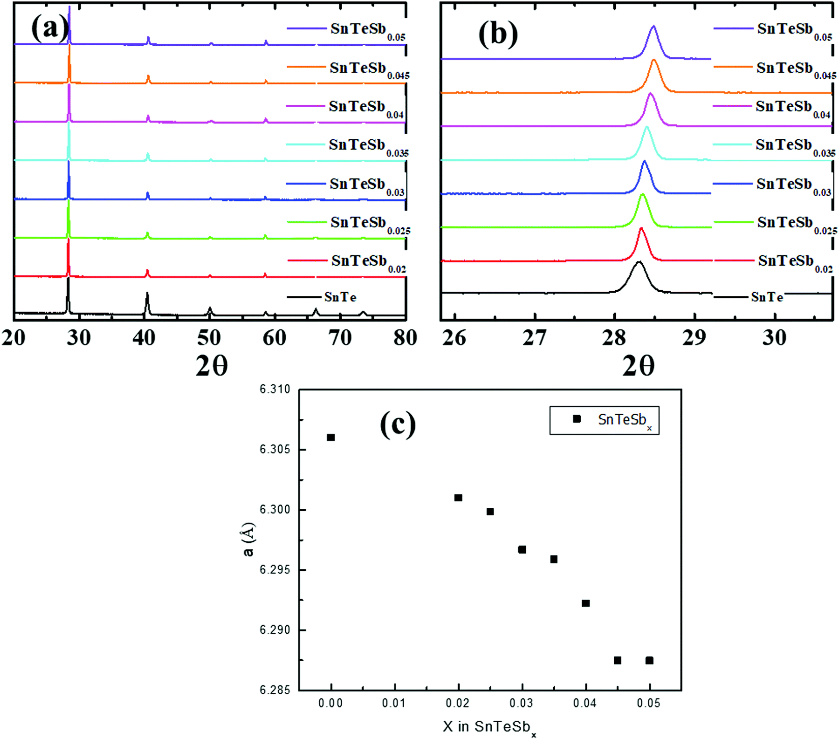
The crystalline ingots of Sb incorporated SnTe, i.e. SnTeSbx (x = 0, 0.02, 0.025, 0.03, 0.035, 0.04, 0.045 and 0.05), were synthesized via a facile melting reaction in a vacuum sealed tube at 1173 K. Powder X-ray diffraction (PXRD) of pristine SnTe and SnTeSbx (x = 0, 0.02, 0.025, 0.03, 0.035, 0.04, 0.045 and 0.05) as shown in Fig. 1(a) can be well indexed to the rock-salt structure of SnTe (Fm![[3 with combining macron]](https://www.rsc.org/images/entities/char_0033_0304.gif) m space group). The pattern shows the absence of the secondary phase within the detection limit of the XRD instrument. The diffraction peaks of varied compositions of SnTeSbx shift to a higher angle with the increase in the concentration of Sb (Fig. 1(b)) suggesting lattice contraction due to the occupancy of large Sn2+ vacancies (radius of 0.93 Å) with a smaller radius Sb3+ (0.76 Å).31 The lattice parameter extracted from the PXRD initially decreases linearly following Vegard's law from a = 6.3 Å to a = 6.28 Å with increasing Sb concentration, which indicates the formation of a solid solution in SnTeSbx (up to x = 0.045). However, the deviation from Vegard's law is prominent for x = 0.05 (Fig. 1(c)). Nevertheless, the non-linear relation between the lattice parameter value and the Sb concentration is not evident in the PXRD pattern which can be due to the low concentration of the secondary phase or nanostructures which is beyond the detection limit of the apparatus.
m space group). The pattern shows the absence of the secondary phase within the detection limit of the XRD instrument. The diffraction peaks of varied compositions of SnTeSbx shift to a higher angle with the increase in the concentration of Sb (Fig. 1(b)) suggesting lattice contraction due to the occupancy of large Sn2+ vacancies (radius of 0.93 Å) with a smaller radius Sb3+ (0.76 Å).31 The lattice parameter extracted from the PXRD initially decreases linearly following Vegard's law from a = 6.3 Å to a = 6.28 Å with increasing Sb concentration, which indicates the formation of a solid solution in SnTeSbx (up to x = 0.045). However, the deviation from Vegard's law is prominent for x = 0.05 (Fig. 1(c)). Nevertheless, the non-linear relation between the lattice parameter value and the Sb concentration is not evident in the PXRD pattern which can be due to the low concentration of the secondary phase or nanostructures which is beyond the detection limit of the apparatus.
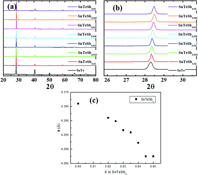 |
| | Fig. 1 (a) X-Ray diffraction patterns of SnTeSbx (x = 0, 0.02, 0.025, 0.03, 0.035, 0.04, 0.045 and 0.05) samples. (b) Enlarged (2 0 0) peak of SnTeSbx indicating the shift towards a higher angle with the increase of Sb concentration. (c) Room temperature lattice constants as a function of x. | |
Detailed microstructure analysis was performed using a scanning electron microscope (SEM) and a high-resolution transmission electron microscope (HRTEM) to investigate the underlying mechanism responsible for the experimentally obtained very low κlat of Sb added SnTe.
The morphology of SnTeSbx characterized by SEM with energy dispersive X-ray spectroscopy (EDX) is shown in Fig. 2. Addition of Sb shows no apparent change in the surface morphology of the SnTe samples. However, the EDX mapping shows that the constituent elements are evenly distributed in the matrix when the concentration of Sb lies within the solubility limit. However, when the addition of Sb is high (beyond the solubility limit), both crystalline and amorphous nanoprecipitates were seen. The quantity of this secondary precipitates increases with the increase in the concentration of Sb. The EDS spectra and the compositional analysis of the nanoprecipitate of the composition SnTeSbx (x = 0, 0.04, 0.045 and 0.05) are shown in S1 in the ESI.† ICP-OES analysis of SnTeSb0.05, carried out to gain an understanding of the composition of the material, shows Sn at 50 at%, Te at 50 at% and Sb at 2 at%.
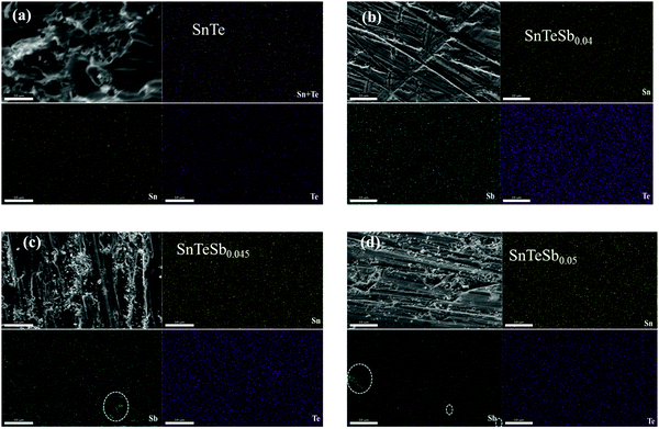 |
| | Fig. 2 SEM image with EDS mapping of (a) SnTe, (b) SnTeSb0.04, (c) SnTeSb0.045 and (d) SnTeSb0.05. | |
The detailed nanoscale examination of SnTeSbx using HRTEM (Fig. 3) shows a single phase microstructure when the concentration of Sb lies within x ≤ 0.04, although the PXRD pattern shows a single phase for all the samples under investigation. Nevertheless, the images of the SPS samples, SnTeSb0.045 and SnTeSb0.05 (Fig. 3(b–d)), are of great interest as these compositions reveal that several nanoscale precipitates were formed which share coherent interfaces with the SnTe matrix and are responsible for low thermal conductivity at higher temperature. The nature of the interface formed between the SnTe matrix and the Sb-nanoprecipitates can be identified from the misfit parameter (δ), which is defined as43
| | | δ = (dSnTe − dSb2Te3) × 100/dSnTe | (3) |
where
d stands for the inter-planer distance. The value of
dSnTe estimated from HRTEM image analyses was found to be ∼0.315 nm. Similarly, HRTEM images yield the value of
dSb2Te3 to be ∼0.3218 nm, which is in agreement with the value obtained from the (015) diffraction peak of Sb
2Te
3.
44 The resultant value of
δ is found to be 2.15%. A low value of
δ (
i.e. <25%) implies the formation of a coherent interface between matrix SnTe and endotaxial Sb
2Te
3 nanoprecipitates.
43Fig. 3(d) clearly reveals the matching of the lattices resulting in the formation of a coherent interface without any dislocations at the grain boundary. Such a coherent interface can contribute to the scattering of phonons with medium and long wavelengths, meanwhile maintaining required carrier transport without unnecessary scattering. Moreover, the mass fluctuation due to the difference in the molecular mass of the host atom Sn (118.71 g mol
−1) and Te (127.6 g mol
−1) and the guest atom Sb (121.76 g mol
−1) creates atomic defects such as dislocation clusters (as shown in
Fig. 3(c)) which contribute to the lattice strain instability and thus reduce the lattice thermal conductivity by scattering the short wavelengths effectively.
45 Thus, these nanoscale features are distinctive in terms of improving the performance of the thermoelectric properties of SnTe. In contrast, when the concentration of Sb is 0.05 at%, the secondary intergrowth is evident in the HRTEM image which is responsible for the overall modification in the chemistry of the SnTe matrix. These nano intergrowths scatter the mid- and long wavelength phonons efficiently through synergistic (i) inter-scattering at the interfaces of the matrix and the nanodomain and (ii) intra-scattering by the intergrowth precipitation. In addition, the point defects due to the presence of Sb scatter the short wavelength phonons and thus, the
x ≥ 0.04 composition shows the lowering of the lattice thermal conductivity at high
T.
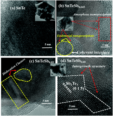 |
| | Fig. 3 HRTEM images of (a) SnTe and (b) SnTeSb0.045 showing different kinds of precipitates. (c) SnTeSb0.05 displays the dislocation clusters due to point defects. (d) SnTeSb0.05 showing the intergrowth precipitate. The inset shows the low resolution images. | |
Another piece of evidence of the formation of Sb2Te3 from the reaction between SnTe and excess Sb beyond the solubility limit is the X-ray photoelectron spectroscopy (XPS) results shown in Fig. 4. The survey XPS spectra for SnTeSb0.05 are shown in Fig. 4(a). In the survey XPS spectra, the signal from each element, such as Sn, Te, and Sb, is seen. In addition, the sample exhibits the presence of physisorbed oxygen (shown as the O 1s peak). All the XPS peaks were calibrated with the C 1s peak position at 284.8 eV. It is observed that the Te/Sb spectrum consists of two characteristic peaks due to spin–orbit splitting, e.g., Te 3d5/2 and Te 3d3/2, which are fitted for 575.6 eV and 586.0 eV respectively (Fig. 4(b)). The systematic shift of the binding energy for Te 3d to higher energies can be attributed to the oxidation status of elemental Te (Te4+ and Te6+), indicating the surface oxidation of Te. However, the systematic shift of the binding energy for Te 3d to lower energies indicates the steadily promoted component of the reduced state for elemental Te (Te2−), suggesting the enhanced content of Sb2Te3.
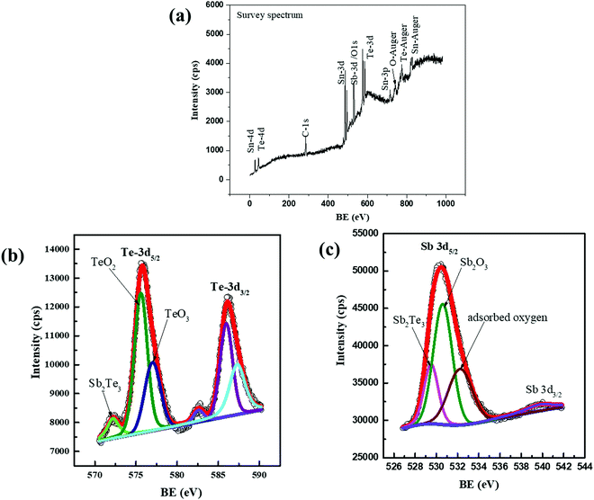 |
| | Fig. 4 XPS spectra of the SnTeSb0.05 sample. (a) Survey spectra indicating the elements present in the sample. (b) High resolution spectra of Te. (c) High resolution spectra of Sb. | |
The Sb 3d spectrum shown in Fig. 4(c) refers to the +3 oxidation state, indicating the non-existence of metallic Sb. Nevertheless, the low electron density near Sb3+ moves the corresponding peak towards higher binding energy. For example, owing to the oxidation of Sb2Te3, the peaks at 529.5 eV (3d5/2) contributed by Sb 3d in Sb2Te3 shift up to 530.6 eV (3d5/2), which corresponds to Sb 3d in Sb2O3. The peak of O 1s at ∼532.2 eV corresponds to the adsorbed oxygen. Thus, combined with the presence of the oxidation peak in the Te 3d spectrum, the formation of TeO2 and TeO3 can be rationally deduced as due to surface oxidation as follows:
| 2Sb2Te3 + 3O2 = 2Sb2O3 + 6Te |
| Te + O2 = TeO2; 2Te + 3O2 = 2TeO3 |
Indication of no oxide phase in the XRD indicates that the oxidation merely occurs on the sample surface. Therefore, it is believed that the inadequate oxidation would not play any influential role in the thermoelectric properties.
3.2. Modification of the band structure via Sb incorporation in SnTe
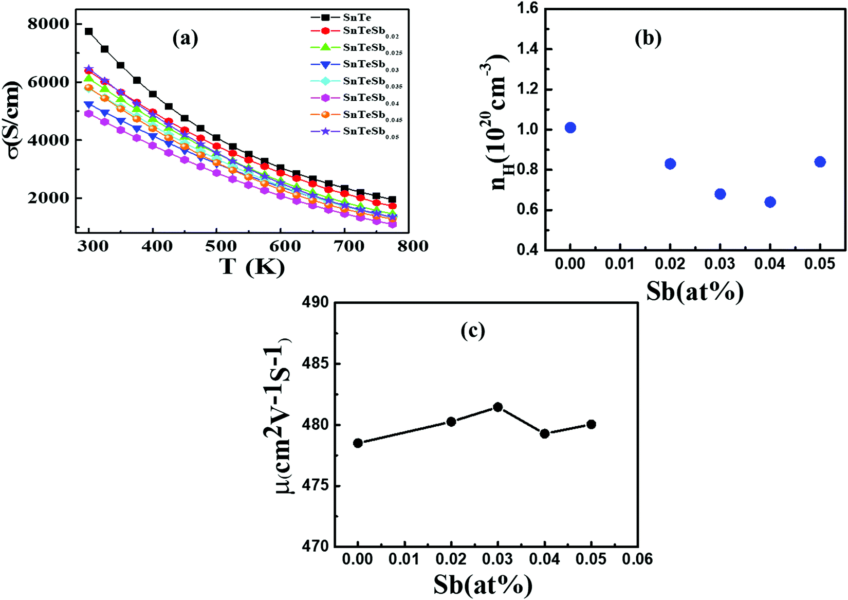
Temperature dependent electrical transport properties are shown in Fig. 5. The trend of electrical conductivity (σ) vs. T (Fig. 5(a)) illustrates degenerate semiconducting behavior, which primarily originates due to intrinsic Sn vacancies.22 In the entire temperature range investigated, σ decreases with the increase in T and shows the typical characteristic of metallic conduction. The value of σ drastically decreases from 7740.5 S cm−1 to 4877.6 S cm−1 for the composition SnTeSb0.04 at room temperature. The gradual reduction of σ with the increase of the donor Sb content is due to systematic reduction of the p-type carrier concentration (nH). In other words, the reduction of the hole concentration (which are primarily responsible for the high conductivity of SnTe) is attributed to their neutralization by aliovalent Sb3+ which is supposed to donate surplus electrons to the system from the chemical valence count.30 However, at room temperature, with the increase of the secondary nanoprecipitates, the σ value increases and shows a value of 6400 S cm−1 for x = 0.05. This observation can be endorsed to the increase in the hole concentration due to the precipitation of the Sb-rich nanodomains. The finding can also be interrelated with the alteration of the chemical composition of the matrix and thereby the change in the hole carrier density. Tan et al. and Banik et al. explicitly mentioned that Sb doping in PbTe and Sb doping in SnTe induces strained endotaxial nanoprecipitates PbmSb2nTem+3n and SnmSb2nTe3n+m respectively.30,46 Using the similar analogy, it is worth mentioning that the non-linearity in Vegard's law and the presence of nanoprecipitates in the matrix with x ≥ 0.04 are due to the formation of intergrowth nanostructures of quasi-binary composition of (SnTe)m(Sb2Te3)n. However, for Banik et al., since Sb was doped at the Sn site, the formation of the secondary intergrowth was evident for Sb content ≥0.1230 and the concentration of the secondary intergrowth precipitate was within the detection limit of XRD. In this study, since Sb was added in excess to the SnTe matrix, the presence of the nano-intergrowth was manifested at a much lower concentration of Sb (x ≥ 0.04) in electron microscopy observation; however, the concentration was beyond the detection limit of PXRD. The Measurement of the Hall carrier density at room temperature shows a positive Hall coefficient value (RH) which indicates p-type conduction. The hole carrier density reduces drastically in Sb-doped SnTe (x ≥ 0.04) from 1.01 × 1020 cm−3 to 6.4 × 1019 cm−3, due to the quenching of the holes. Nevertheless, the hole density shows enhancement for x = 0.05 (Fig. 5(b)), which is correlated to the change in the matrix system due to the nanostructured intergrowth as mentioned earlier. The hole mobility measured by  was plotted as a function of Sb concentration (Fig. 5(c)). As described by Banik et al., not much variation is seen in the carrier mobility especially at lower Sb addition, which indicates that the nanoprecipitates are endotaxial in nature, and so the interfaces are transparent for the electrons.30
 |
| | Fig. 5 (a) Electrical conductivity of SnTeSbx as a function of T. (b) Carrier concentration as a function of Sb concentration at room temperature. (c) Change in mobility with the increase in Sb concentration at 300 K. | |
Fig. 6(a) shows the temperature dependence of the Seebeck coefficient (S) of SnTeSbx (x = 0, 0.02, 0.025, 0.03, 0.035, 0.04, 0.045 and 0.05). The positive value of S indicates the dominating p-type conduction in the investigated temperature range of 300–800 K, which is consistent with the sign of Hall carrier concentration. The pristine SnTe, i.e. x = 0, sample possesses a low Seebeck coefficient of ∼34 μV K−1 at room temperature because of its high hole concentration as stated above. Remarkably, the room temperature Seebeck coefficient decreases gradually with the increase in x, i.e. with the alloying of Sb, despite the reduction of hole concentration, which is contradictory to the typical behavior expected for a p-type semiconductor. This strange variation in the Seebeck coefficient is related to the distinctive character of the two non-degenerate valence bands (at the L and Σ points of the Brillouin zone) of SnTe. For the two-valence band case, the total Seebeck coefficient is given by eqn (4),
| | 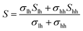 | (4) |
where
Slh and
Shh denote the Seebeck coefficient of the light hole band and heavy hole band respectively, while
σlh and
σhh denote the electrical conductivity from light hole band and heavy hole band contribution, respectively.
14 Due to the high hole density in pristine SnTe, the Fermi level lies in the valence band, closer to the heavy-hole band and is energetically low. However, with decreasing hole concentration in SnTeSb
x (
x = 0, 0.02, 0.025, 0.03, 0.035, 0.04, 0.045 and 0.05), the Fermi level rises and gradually shifts away from the heavy-hole band. Thus, only the light-hole band contributes to the Seebeck coefficient
28 with feeble participation of the heavy hole band in the transport properties. In accordance with the statement, the
S–
T plot depicts that at lower temperature, the Seebeck coefficient is maximum for the pristine SnTe and shows the minimum value for
x = 0.05 at%. To further clarify the reduction of the Seebeck coefficient,
S, the effective mass (
m*) of the carriers was calculated for SnTeSb
x using the experimental
S and carrier density (
nH) measured at 300 K, by the following expressions (
eqn (5)–(7)):
| |  | (5) |
| |  | (6) |
| |  | (7) |
where
r,
e,
h,
kB,
η and
Fn(
η) are the scattering factor, electron charge, Planck's constant, the Boltzmann constant, reduced Fermi energy and
nth order Fermi integral respectively. The reduced Fermi energy was computed by fitting the resultant experimental Seebeck data. The
m* values were evaluated based on the single parabolic band model, where, for simplicity,
r = −1/2 was considered for acoustic phonon scattering. The estimated
m* value of pristine SnTe was 0.36
m0, which reduces to 0.15
m0 for the composition SnTeSb
0.05 and thereby indicates the predominant participation of the light (L) valence band at 300 K for the Sb added SnTe.
47
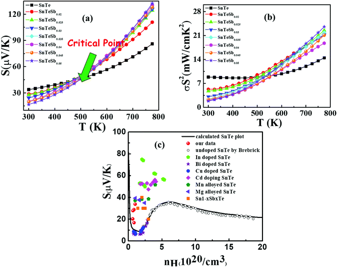 |
| | Fig. 6 (a) Temperature dependent Seebeck coefficient of SnTeSbx highlighting the critical point. (b) Temperature dependent power factor calculated from the experimentally determined Seebeck coefficient and electrical conductivity. (c) Carrier concentration dependent Seebeck coefficients for SnTeSbx at room temperature. The solid curve represents the theoretical Pisarenko curve based on the VBM model. For comparison, previously reported S vs. n experimental data of undoped SnTe, In-doped SnTe,19 Bi doped SnTe,57 Cu-doped SnTe,56 Cd doped SnTe,28 Mn alloyed SnTe,58 Mg alloyed SnTe55 and Sb doped SnTe were included in the Pisarenko plot. | |
Surprisingly, the SnTeSbx samples with lower Seebeck coefficients at lower temperature show higher Seebeck coefficient when the temperature is ∼473 K (designated as critical temperature here) (Fig. 6(a)). The brisk rise of the Seebeck coefficient at T > 473 K is evocative of the similar but more noticeable behavior of p-type PbTe, and is attributed to the enhanced contribution of the heavy hole Σ band at higher temperatures due to thermal excitations. Aggarwal et al. have explicitly mentioned in an article that in the temperature range of 300–473 K, SnTe alloys exhibit a local ferroelectric domain. However, the concrete vindication of the relation between the critical temperature and the local ferroelectric instability has not been understood.48 Similar to PbTe, in SnTe, the valence band is formed by the Te orbital, while Sn constitutes the conduction band due to the difference in the electronegativity, χ, of Sn (χSn = 1.96, in the Pauling electronegative scale) and Te (χTe = 2.10).18 Aliovalent dopant Sb forms the donor impurity states immediately below the conduction band, because of the slightly lower values of the electronegativity, χSb = 2.05, compared to Te, which thus reduces the principal band gap.49
However, the contribution of the heavy hole Σ band in the high temperature properties of SnTe is better demonstrated once a substantial number of Sn vacancies have been removed. In other words, alloying of Sb in SnTe alters the electronic structure of SnTe as explained using DFT calculations in the later section. Sb reduces the band offset (ΔEL–Σ) and thereby causes the band convergence and, beyond the critical temperature, promotes the conduction of the heavy hole valence band and enhances S with increasing x at higher temperature.49,50 The understanding of the effect of weak band convergence by Sb is in good agreement with X. Tan et al., where Bi and Sb were classified as elements contributing to band convergence in SnTe and PbTe.51 A similar observation in Sn-self compensated SnTe was reported by Tan et al., where the support for the contribution of the heavy hole Σ band at higher temperature was shown in Hall coefficient measurements as a function of time. The RH–T plot shows a peak at the critical temperature (∼500 K) as observed in the S–T plot and is probably due to the onset of the Σ-band contribution in the transport properties.28 This anomaly has also been observed in p-type skutterudites and other Pb-chalcogenides.13,52–54
Fig. 6(b) depicts the power factors (P.F.'s) for all SnTeSbx samples. The pristine SnTe has a relatively high P.F. of ∼9 μW cm−1 K−2 at 300 K mainly benefiting from its very high electrical conductivity. The P.F.'s deteriorate upon Sb addition in the low temperature range (T < 470 K) due to the simultaneously decreased electrical conductivities and Seebeck coefficients, but above 470 K, there is a greatly enhanced Seebeck coefficient for the hole compensated Sb added SnTe samples and the P.F.'s improve with respect to SnTe itself. At 775 K, the P.F. of SnTeSb0.05 shows 71% enhancement as compared to the pristine SnTe.
The room temperature Pisarenko plot of the Seebeck coefficient (S) as a function of carrier concentration (nH) of SnTeSbx samples is shown in Fig. 6(c). The theoretical Pisarenko plot was constructed as a function of carrier density (the solid line in the curve) based on the two-valence band model (VBM) of SnTe by Zhang et al. which considers the nonparabolicity of the light-hole band. The model was calculated using a light-hole band (L) effective mass of ∼0.168me, a heavy-hole band (Σ) effective mass of ∼1.92me and an energy offset, ΔEL–Σ, between the two valence bands of 0.35 eV, respectively.19 For comparison, the present S vs. nH data of SnTeSbx samples at room temperature were considered with previously reported values of Cd,28 Mg,55 Cu,56 Bi,57 Mn,58 and In19 doped SnTe. The results obtained indicate the validity of the VBM of SnTe. The S value reported by Zhang et al. lies far above the theoretical prediction and is claimed to appear due to the resonant state formation near the Fermi level induced by the indium dopant. Other SnTe samples are in good agreement with the VBM model, indicative of conventional doping behavior. The experimental room temperature S values of Sb-added SnTe samples reside slightly above the Pisarenko curve. This originates probably due to the mass fluctuation which causes disturbance in the electric potential at the interfaces between two dissimilar structures or elements and causes energy dependent scattering of carriers, leading to an energy filtering effect and weak valence band convergence.32,59 This enhances the Seebeck coefficient; a similar trend has been earlier observed for Sb doped SnTe and Sb and Ge co-doped SnTe alloys.30,60
In order to elucidate comprehensively the role of incorporation of Sb in the band structure of SnTe, DFT calculations were performed on its electronic band structure and was subsequently compared with pristine SnTe. Pristine SnTe is known to possess a principal band gap between the light hole valence and conduction bands at the L point which folds on to the Γ point (Fig. 7(a)) in the current tetragonal supercell.61 This band gap is estimated to be 0.08 eV which agrees well with the previous results, although with a typical underestimation compared to the experimental band gap of 0.18 eV due to the existence of discontinuity in the derivative of energy with respect to number of electrons.17,18 The projected density of states (pDOS) reveals that the valence band is typically formed by the Te ‘p’ states while the conduction band is formed by the Sn ‘p’ states (Fig. 7(b)). One of the reasons for the poor performance of SnTe is the large separation between the light hole and heavy hole valence sub-bands.62 The heavy hole valence sub-band which typically occurs at the Σ point of the Brillouin zone of the primitive cell occurs at the Z + δ point in the Z → R direction in the current supercell due to folding of the bands.61 An energy offset of 0.30 eV is observed between the light hole valence band at the Γ point and the heavy hole valence band at the Z + δ point in the present case preventing the participation of the heavy hole valence band in the transport properties at lower temperatures.63 On the other hand, the energy offset between the light hole (at the Γ point) and the heavy hole (at the Z + δ point) conduction bands is observed to be 0.24 eV. Incorporation of Sb in the SnTe matrix leads to the direct band gap at the Γ point reducing to 0.038 eV (Fig. 7(c)). This reduction in the band gap is due to the 8 fold degenerate conduction bands losing degeneracy to form 4 sets of doubly degenerate bands and splitting off of the lower most doubly degenerate band, capping the top of the valence band as seen previously in the case of the Bi resonant dopant.63 Up until now, Sb was known to optimize the hole carrier concentration and reduce the thermal conductivity.30,64 The interesting feature here is the reduction in the energy offset between the light hole and heavy hole valence as well as conduction bands leading to the band convergence phenomenon by Sb which was not reported previously by Banik et al.30 The energy difference in the valence band area reduces to 0.26 eV while the heavy hole conduction band appears 0.1 eV above the lowest point in the light hole region. The convergence of the valence sub-bands is clearly observed as the increase in the DOS at the valence band edge (Fig. 7(d)). Such an increase in the DOS is previously seen in the case of convergence caused due to Mg and Ca dopants.29,35 In Sb incorporated SnTe the valence band is contributed by Te ‘p’ orbitals while the conduction band has contributions from ‘p’ orbitals of Sn and Sb. The pDOS reveals that the hybridization of Sb ‘p’ orbitals with Sn ‘p’ orbitals in the conduction band region leads to the reduction in the band gap and the conduction band convergence. The hybridization also gives rise to hyper deep defect states within the valence band region. Although the convergence value of 0.04 eV seems too small to have any effect on the transport properties at lower temperatures, as the temperature increases this value increases as the heavy hole band further rises in energy as seen previously in the case of PbTe to cause a considerable effect.14 The number of degenerate valleys contributing at the higher temperature increase from 4 contributed by the light hole valence bands at the Γ point to 16 due to the addition of 12 valleys contributed by the heavy hole valence band at the Z + δ point in the Z → R direction in the Brillouin zone. The result of this is the increase in the density of states effective mass which is directly proportional to the Seebeck coefficient.35 The contribution by the heavy hole valence band further increases with the increase in the amount of dopant added.49 Hence, at higher temperature, experimentally an increase in the Seebeck value is observed with the increase in the Sb content.
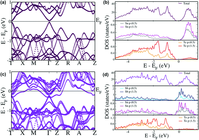 |
| | Fig. 7 Electronic structures and pDOS of (a and b) SnTe and (c and d) Sb incorporated SnTe. Energies are shifted with respect to the Fermi level which is set to zero. | |
3.3. Analysis of the thermal transport properties and zT of Sb added SnTe
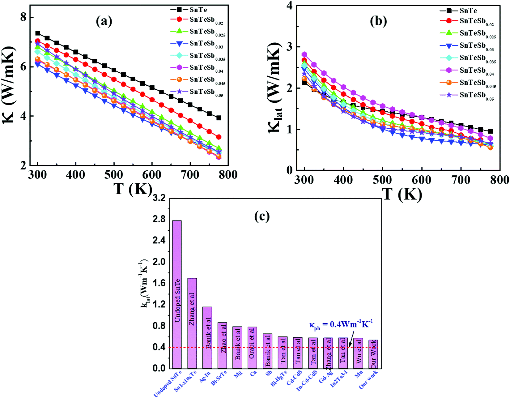
The other problem, which needs to be resolved, is the high thermal conductivity induced by the intrinsic Sn vacancies, which also provoke high electrical conductivity. Fig. 8(a) presents the temperature dependent total thermal conductivity (κtotal) of SnTeSbx (x = 0, 0.02, 0.025, 0.03, 0.035, 0.04, 0.045 and 0.05) which is essentially a combination of two components: the lattice contribution (κlat) and the electronic contribution (κele) which also includes the bipolar conduction. The electronic contribution can be estimated by the Wiedemann–Franz relation κele = LσT, where L is the Lorenz number, σ is the electrical conductivity, and T is the absolute temperature. In this report, the L value was obtained from the accepted methodology of fitting the Seebeck data to the reduced chemical potential and the details are shown in ESI,† S2.65 The lattice thermal conductivity (κlat) is then computed by subtracting the electronic contribution of the thermal conductivity from κtotal and the results are shown in Fig. 8(b). Alloying of Sb in SnTe reduces κtotal from 7.33 W m−1 K−1 to 6.09 W m−1 K−1 for SnTeSb0.3 at 300 K, which is ∼17% as compared to pristine SnTe. However, the composition x = 0.045 at% and 0.05 at% shows higher κtotal at room temperature. This can be attributed to the dominating nature of the electronic part of the thermal conductivity at low T. With increasing temperature, κtotal decreases rapidly without indicating any bipolar effect, and is in harmony with the behavior of the S vs. T plot. No onset of the bipolar diffusion also corroborates the fact that Sb incorporation opens the thermal band gap and reduces the value of bipolar thermal conductivity (κbip). This is logical because κbip is related to the band gap (Eg) through eqn (8):66| |  | (8) |
Here, A and n are two variable parameters and kB is the Boltzmann constant. The total thermal conductivities of all Sb-added SnTe are lower than that of the undoped sample. Moreover, at high temperature, when the acoustic phonon scattering is high, the κtotal of 0.05 at% Sb reduces substantially from 6.95 W m−1 K−1 at 300 K to 2.56 W m−1 K−1 at 800 K which is 63% reduction as compared to pristine SnTe which shows a reduction of ∼47%. This enormous reduction in κtotal is due to the reduction of κel caused due to the quenching of the intrinsic Sn-vacancies and simultaneously the reduction of κlat due to the increased phonon scattering at different length scales. The various mechanisms that were successfully implemented to scatter the wide spectrum of phonons within the working temperature range and are responsible for the ultralow lattice thermal conductivity of the Sb-added SnTe are discussed below:
 |
| | Fig. 8 Temperature dependent (a) total and (b) lattice thermal conductivities of SnTeSbx. (c) Comparison of lattice thermal conductivities between undoped SnTe,19 Sn1−xInTe,19 Ag–In codoped SnTe,72 Bi–SrTe co-doped SnTe,73 Mg alloyed SnTe,55 Ca alloyed SnTe,74 Sb doped SnTe,30 Bi–HgTe co-doped SnTe,75 Cd–CdS co-doped SnTe,28 In–Cd–CdS co-doped SnTe,76 Gd–Ag co-doped SnTe,77 In2Te3–I co-doped SnTe,78 Mn alloyed SnTe79 and our work. The dotted line shows the proximity to the theoretical limit of κlat = 0.4 W m−1 K−1 for SnTe calculated by the model proposed by Cahill et al.71 | |
(i) Grain boundary scattering.
Grain boundaries were employed as phonon scatterers in scheming the TE materials. The association between the grain size (characterized length), phonon coherencies, wavelength, and mean free path has an influence on dispersion of phonons. Thermal conductivity reduces when the actual phonon mean free path is greater than the crystal or grain size.67 Since the mean free path of the phonon is a function of wavelength, and wavelength itself is related to temperature by Wien's displacement law, i.e. λmaxT = constant, thus, grain boundaries are important scattering sources at low T.59 The microstructural analysis in the present study reveals the presence of several secondary nanoprecipitates, both crystalline and amorphous. These precipitates form both coherent and incoherent interfaces which scatter the phonons effectively and thus reduce the lattice thermal conductivity.
(ii) Point defect scattering.
Aliovalent or isovalent ion doping is advantageous for the modulation of the electronic transport property by band engineering and thermal properties by reducing the thermal conductivity.61,63 These ionic (aliovalent or isovalent) doping are expected to be the first and foremost contributors of charge carriers whereby they usually slash the formation energies of the vacancies propelled by the compensation of the charge carriers.68 Thus, the vacancies are stabilized either near the dislocations or at the interfaces.69,70 Moreover, any dopants or additives with different atomic sizes and masses trigger the stress–strain and mass fluctuations. With the increase in temperature, the wavelength of the phonon decreases and so the short wavelength phonons are scattered effectively by mass fluctuation defects such as the presence of impurities, vacancies, dislocations and alloy atoms. In addition, the mass fluctuation also has an impact on the group velocities. In accordance with eqn (9), the group velocity decrease for high atomic mass impurity elements/dopants/weak chemical bonds is given by| |  | (9) |
where Vs is the speed of the sound in solids and is also considered as the group velocity of phonons, ρ is the density and E is the strength of the chemical bonding.68 The HRTEM analysis shows the presence of dislocation clusters due to the excess addition of aliovalent Sb in SnTe. These clusters are responsible for the scattering of the short wavelength phonons.
(iii) Lattice anharmonicity.
Lattice anharmonicity exists in all materials as an intrinsic scattering character due to phonon–phonon Umklapp scattering which lowers the relaxation time for phonons with the entire range of frequencies. According to Slack, thermal conductivity is given by eqn (10):66,68| |  | (10) |
where M is the average atomic mass (in amu), θD is the Debye temperature, ![[V with combining macron]](https://www.rsc.org/images/entities/i_char_0056_0304.gif) is the average atomic volume (in cubic angstrom), T is the absolute temperature, γ is the Gruneisen parameter measuring the strength of lattice anharmonicity, n is the number of atoms in the primitive cell, and A is a collection of physical constants; A ≈ 3.04 × 10⁻⁶ and κL is in W m−1 K−1. This implies that a large number of atoms in the primitive cell (n) and a strong anharmonicity (γ) are effective for maintaining low κlat, and that κlat decreases with a rise in temperature. Thus, the strength of lattice anharmonicity is crucial as it reduces the lattice thermal conductivity and empowers the performance of thermoelectric materials. Experimental and theoretical analysis shows that SnTe exhibits strong anharmonicity and is strongly correlated to the ferroelectric instability,48,68 which causes robust coupling of acoustic and optical phonons and thus reduces the phonon relaxation time significantly. The coupling effect originates from the presence of soft transverse optical (TO) mode predominantly at the Γ point in the Brillouin zone.16,68 These optical phonon modes contain very low group velocities which, if neglected, lead to underestimation of κlat. However, the optical phonons contribute in the three-electron process and cause added scattering with acoustic phonons and thus reduce the lattice thermal conductivity. Alloying of Sb in SnTe reduces κlat further and is attributed to the lone pair of the 5s orbital of the Sb atom. Moreover, Lee et al. explicitly mentioned that in addition to IV–VI alloys, group V elements such as Bi and Sb also show resonant bonding which leads to long range interactions and consequently lowers the lattice part of the thermal conductivity.16 In fact, the experimental κlat obtained in the present study shows an ultralow κlat value which is in proximity to the theoretical limit of κlat = 0.4 W m−1 K−1 for SnTe when calculated by the model proposed by Cahill et al.71 Surprising, the lowest lattice thermal conductivity reported for high Sb content SnTe, is less than the value reported for Hg-, Mn-, In,- Mg-, Cd- doped SnTe and several co-doped SnTe system Fig. 8(c).19,55,72–79 This is endorsed by the precipitation of Sb2Te3 (as seen in microstructural analysis) which also demonstrates the existence of resonant bonding.16
is the average atomic volume (in cubic angstrom), T is the absolute temperature, γ is the Gruneisen parameter measuring the strength of lattice anharmonicity, n is the number of atoms in the primitive cell, and A is a collection of physical constants; A ≈ 3.04 × 10⁻⁶ and κL is in W m−1 K−1. This implies that a large number of atoms in the primitive cell (n) and a strong anharmonicity (γ) are effective for maintaining low κlat, and that κlat decreases with a rise in temperature. Thus, the strength of lattice anharmonicity is crucial as it reduces the lattice thermal conductivity and empowers the performance of thermoelectric materials. Experimental and theoretical analysis shows that SnTe exhibits strong anharmonicity and is strongly correlated to the ferroelectric instability,48,68 which causes robust coupling of acoustic and optical phonons and thus reduces the phonon relaxation time significantly. The coupling effect originates from the presence of soft transverse optical (TO) mode predominantly at the Γ point in the Brillouin zone.16,68 These optical phonon modes contain very low group velocities which, if neglected, lead to underestimation of κlat. However, the optical phonons contribute in the three-electron process and cause added scattering with acoustic phonons and thus reduce the lattice thermal conductivity. Alloying of Sb in SnTe reduces κlat further and is attributed to the lone pair of the 5s orbital of the Sb atom. Moreover, Lee et al. explicitly mentioned that in addition to IV–VI alloys, group V elements such as Bi and Sb also show resonant bonding which leads to long range interactions and consequently lowers the lattice part of the thermal conductivity.16 In fact, the experimental κlat obtained in the present study shows an ultralow κlat value which is in proximity to the theoretical limit of κlat = 0.4 W m−1 K−1 for SnTe when calculated by the model proposed by Cahill et al.71 Surprising, the lowest lattice thermal conductivity reported for high Sb content SnTe, is less than the value reported for Hg-, Mn-, In,- Mg-, Cd- doped SnTe and several co-doped SnTe system Fig. 8(c).19,55,72–79 This is endorsed by the precipitation of Sb2Te3 (as seen in microstructural analysis) which also demonstrates the existence of resonant bonding.16
The temperature dependence of figure of merit values (zT) of the SnTeSbx (x = 0, 0.02, 0.03, 0.04, and 0.05) samples is shown in Fig. 9(a). zT at high temperatures increases with the concentration of Sb. The highest zT of ∼0.71 is obtained in SnTeSb0.05 at 773 K, due to the synergism of band convergence and ultra-low lattice thermal conductivity. A significant improvement in zT was seen for SnTeSb0.05 which was calculated to be ∼154% increment compared to our pristine SnTe. Finally, the ZT of the TE device, having a finite temperature difference ΔT = Th − Tc, expressed from the maximum efficiency (η) of a single thermoelectric leg, was computed according to eqn (11):80,81
| |  | (11) |
where the highest conversion efficiency (
η) was calculated by using
eqn (12):
| |  | (12) |
using the temperature-dependent parameters
S(
T),
σ(
T), and
κ(
T) between
Th and
Tc. Further,
Fig. 9(b) shows the temperature-dependent efficiency and calculated device
zT of SnTeSb
x and all the samples have shown an improvement of device
zT with increasing Sb incorporation in SnTe. However, the highest device
zT was shown when the Sb addition is within the solubility limit (
Fig. 9(c)). Finally, the device
zT value of 0.14307 at 775 K has been obtained for SnTeSb
0.03 and SnTeSb
0.035, which is ∼44.5% higher than the value 0.09903 at 775 K of pristine SnTe. The exact calculation of maximum efficiency is explained in the spreadsheet S.3.1–S.3.7 for download in ESI.
† Finally, the maximum conversion efficiency has been observed to be increased to 2.9% for SnTeSb
0.03. The significant improvement of 45% in device efficiency is promising for considering these materials as an appropriate substitute to Pb-based chalcogenides. This is the first study to achieve eco-friendly and cost effective SnTe based alloys having moderate
zT via facile and controllable single step methodology without the utilization of any toxic or precious element doping. The high performance benefits the potential of the realization of proficient thermoelectric modules with SnTe as a p-type thermoelement. Nevertheless, the actual application of the device should exhibit genuine feasibility for energy claims such as output voltage, current density, power density, actual device illustrations,
etc.82Table 1 summarizes some of the recent advances of mid-temperature based thermoelectric materials, particularly those with band convergence or resonant states having high
zT values. Thermoelectric generators based on these alloys ought to be explored in future.
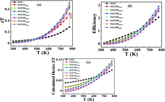 |
| | Fig. 9 Temperature dependent (a) zT values of the different compositions of Sb-added SnTe which reveal an increment of 154% when compared with the undoped SnTe. (b) Theoretical maximum conversion efficiency of SnTeSbx. (c) Comparison of device zT for the different compositions of SnTeSbx. | |
Table 1 Recent advances in medium temperature based thermoelectric materials
| Alloy |
Band structure modification |
Microstructure engineering |
Peak zT |
Ref. |
| Pb0.98Bi0.02Se |
Tuning of EF of PbSe by Bi substitution |
High density of dislocations and pores |
>1.5 |
83
|
| Ge0.85Bi0.05Sb0.10Te |
Valence band convergence |
Nanoprecipitates formed by Bi and Sb create solid solution point defects in GeTe |
1.8 at 725 K |
47 and 84
|
| Ge0.9Sb0.1Te |
Promoting the crystal symmetry of GeTe to enlarge the band degeneracy while flattening the valence band |
Introducing mass fluctuation and point defects to intensify phonon scattering |
1.8 at 773 K |
84 and 85
|
| Ge0.9Sb0.1Te |
Carrier optimization and band structure modulation |
Sb substitution created multiple forms of strain near the defect centre, the herringbone domain structure, and widened tensile/compressive domain boundaries |
2.35 near ∼800 K |
84 and 86
|
| Ge0.87Sn0.05Sb0.08Te |
Carrier optimization and Rashba effect |
Co-existence of grain boundaries, nanoprecipitates, and stacking faults |
2.2 near ∼800 K |
84 and 87
|
| Cd-Doped SnSe |
Cation vacancy engineering |
Localized crystal imperfections including localized lattice distortions and strains, dis-locations, and nanoscale vacancy domains |
1.7 at 823 K |
88
|
| Polycrystalline Na0.03Sn0.965Te |
Intrinsic crystal symmetry |
Softened phonon frequency |
3.1 at 783 K |
89
|
4. Conclusions
In conclusion, a simple methodology was adapted to synthesize inexpensive, eco-friendly Sb-added SnTe via a single-step melting route. Sb causes carrier optimization along with induction of band convergence by favorably altering the band structure. Mass contrast causes disturbance in the electric potential at the interfaces between two dissimilar elements leading to an energy filtering effect which altogether enhances the Seebeck coefficient. Incorporation of Sb in excess leads to the precipitation of intergrowth which forms a coherent interface with the matrix. The lattice thermal conductivity reduces remarkably and is in proximity to the amorphous limit owing to scattering by grain boundaries, point defects and lattice anharmonicity. Integration of the approaches synergistically modulates the electronic and thermal transport properties of polycrystalline SnTe with no addition of precious and toxic dopants. This kind of cost-effective high-performance material is suitable for the fabrication of budget thermoelectric modules and makes them a suitable alternative to the conventional PbTe based alloys.
Conflicts of interest
There is no conflict of interest.
Acknowledgements
The author RB would like to acknowledge Dr K. P. Muthe and the entire Thin Film Devices Section (TFDS) for providing their support and valuable inputs for this article. SN acknowledges the FRGS (Grant No. GGSIPU/DRC/FRGS/2020/1988/9). The author (USS) acknowledges the grant in the form of DST INSPIRE Faculty award from the Department of Science and Technology, Government of India. The authors also thank the National Physical Laboratory, New Delhi, for consolidation of the sample using Spark Plasma Sinter and founder Chancellor Bhagawan Sri Sathya Sai Baba and Trustees/Administrators for providing characterization facilities at Central Research Instruments Facility (SSSIHL-CRIF).
References
-
A. F. Ioffe, L. S. Stil'bans, E. K. Iordanishvili, T. S. Stavitskaya, A. Gelbtuch and G. Vineyard, Semiconductor Thermoelements and Thermoelectric Cooling, 1957 Search PubMed.
- G. J. Snyder and E. S. Toberer, Nat. Mater., 2008, 7, 105–114 CrossRef CAS PubMed.
- R. Basu, S. Bhattacharya, R. Bhatt, M. Roy, S. Ahmad, A. Singh, M. Navaneethan, Y. Hayakawa, D. Aswal and S. Gupta, J. Mater. Chem. A, 2014, 2, 6922–6930 RSC.
- K. Biswas, J. He, Q. Zhang, G. Wang, C. Uher, V. P. Dravid and M. G. Kanatzidis, Nat. Chem., 2011, 3, 160–166 CrossRef CAS PubMed.
- L. Bjerg, B. B. Iversen and G. K. Madsen, Phys. Rev. B: Condens. Matter Mater. Phys., 2014, 89, 024304 CrossRef.
- S. N. Guin, A. Chatterjee, D. S. Negi, R. Datta and K. Biswas, Energy Environ. Sci., 2013, 6, 2603–2608 RSC.
- R. Basu and A. Singh, Mater. Today Phys., 2021, 100468 CrossRef CAS.
- S. Lin, W. Li, Z. Chen, J. Shen, B. Ge and Y. Pei, Nat. Commun., 2016, 7, 1–6 Search PubMed.
- L.-D. Zhao, S.-H. Lo, Y. Zhang, H. Sun, G. Tan, C. Uher, C. Wolverton, V. P. Dravid and M. G. Kanatzidis, Nature, 2014, 508, 373–377 CrossRef CAS PubMed.
- L.-D. Zhao, G. Tan, S. Hao, J. He, Y. Pei, H. Chi, H. Wang, S. Gong, H. Xu and V. P. Dravid, Science, 2016, 351, 141–144 CrossRef CAS PubMed.
- S. N. Guin, J. Pan, A. Bhowmik, D. Sanyal, U. V. Waghmare and K. Biswas, J. Am. Chem. Soc., 2014, 136, 12712–12720 CrossRef CAS PubMed.
- H. Liu, X. Shi, F. Xu, L. Zhang, W. Zhang, L. Chen, Q. Li, C. Uher, T. Day and G. J. Snyder, Nat. Mater., 2012, 11, 422–425 CrossRef CAS PubMed.
- Y. Pei, H. Wang and G. J. Snyder, Adv. Mater., 2012, 24, 6125–6135 CrossRef CAS PubMed.
- Y. Pei, X. Shi, A. LaLonde, H. Wang, L. Chen and G. J. Snyder, Nature, 2011, 473, 66–69 CrossRef CAS PubMed.
- S. Ahmad, A. Singh, S. Bhattacharya, M. Navaneethan, R. Basu, R. Bhatt, P. Sarkar, K. N. Meshram, A. K. Debnath and K. P. Muthe, ACS Appl. Energy Mater., 2020, 3, 8882–8891 CrossRef CAS.
- S. Lee, K. Esfarjani, T. Luo, J. Zhou, Z. Tian and G. Chen, Nat. Commun., 2014, 5, 1–8 CrossRef PubMed.
- U. S. Shenoy and D. K. Bhat, J. Mater. Chem. C, 2019, 7, 4817–4821 RSC.
- D. K. Bhat and U. S. Shenoy, Mater. Today Phys., 2019, 11, 100158 CrossRef.
- Q. Zhang, B. Liao, Y. Lan, K. Lukas, W. Liu, K. Esfarjani, C. Opeil, D. Broido, G. Chen and Z. Ren, Proc. Natl. Acad. Sci. U. S. A., 2013, 110, 13261–13266 CrossRef CAS PubMed.
- S. Mandava, R. Basu, B. Khasimsaheb, S. Bathula, A. Singh and S. Neeleshwar, Mater. Adv., 2021, 2, 4352–4361 RSC.
- G. Tan, F. Shi, S. Hao, L.-D. Zhao, H. Chi, X. Zhang, C. Uher, C. Wolverton, V. P. Dravid and M. G. Kanatzidis, Nat. Commun., 2016, 7, 1–9 Search PubMed.
- R. Moshwan, L. Yang, J. Zou and Z. G. Chen, Adv. Funct. Mater., 2017, 27, 1703278 CrossRef.
- J. Dimmock, I. Melngailis and A. Strauss, Phys. Rev. Lett., 1966, 16, 1193 CrossRef CAS.
- L. Rogers, J. Phys. D: Appl. Phys., 1968, 1, 845 CrossRef.
- Y. Pei, L. Zheng, W. Li, S. Lin, Z. Chen, Y. Wang, X. Xu, H. Yu, Y. Chen and B. Ge, Adv. Electron. Mater., 2016, 2, 1600019 CrossRef.
- W. Li, Z. Chen, S. Lin, Y. Chang, B. Ge, Y. Chen and Y. Pei, J. Materiomics, 2015, 1, 307–315 CrossRef.
- D. J. Singh, Funct. Mater. Lett., 2010, 3, 223–226 CrossRef CAS.
- G. Tan, L.-D. Zhao, F. Shi, J. W. Doak, S.-H. Lo, H. Sun, C. Wolverton, V. P. Dravid, C. Uher and M. G. Kanatzidis, J. Am. Chem. Soc., 2014, 136, 7006–7017 CrossRef CAS PubMed.
- D. K. Bhat and S. Shenoy U, J. Phys. Chem. C, 2017, 121, 7123–7130 CrossRef CAS.
- A. Banik, B. Vishal, S. Perumal, R. Datta and K. Biswas, Energy Environ. Sci., 2016, 9, 2011–2019 RSC.
- X. Li, J. Liu, S. Li, J. Zhang, D. Li, R. Xu, Q. Zhang, X. Zhang, B. Xu and Y. Zhang, Nano Energy, 2020, 67, 104261 CrossRef CAS.
- Z. Ma, C. Wang, Y. Chen, L. Li, S. Li, J. Wang and H. Zhao, Mater. Today Phys., 2021, 17, 100350 CrossRef CAS.
- S. K. Kihoi, J. N. Kahiu, H. Kim, U. S. Shenoy, D. K. Bhat, S. Yi and H. S. Lee, J. Mater. Sci. Technol., 2021, 85, 76–86 CrossRef.
- S. K. Kihoi, H. Kim, H. Jeong, H. Kim, J. Ryu, S. Yi and H. S. Lee, J. Alloys Compd., 2019, 806, 361–369 CrossRef CAS.
- D. K. Bhat and U. S. Shenoy, Mater. Today Phys., 2018, 4, 12–18 CrossRef.
- T. Hussain, X. Li, M. H. Danish, M. U. Rehman, J. Zhang, D. Li, G. Chen and G. Tang, Nano Energy, 2020, 73, 104832 CrossRef CAS.
- D. Spitzer, J. Phys. Chem. Solids, 1970, 31, 19–40 CrossRef CAS.
- K. Shportko, S. Kremers, M. Woda, D. Lencer, J. Robertson and M. Wuttig, Nat. Mater., 2008, 7, 653–658 CrossRef CAS PubMed.
- O. Delaire, J. Ma, K. Marty, A. F. May, M. A. McGuire, M.-H. Du, D. J. Singh, A. Podlesnyak, G. Ehlers and M. Lumsden, Nat. Mater., 2011, 10, 614–619 CrossRef CAS PubMed.
- M. Zhou, Z. M. Gibbs, H. Wang, Y. Han, C. Xin, L. Li and G. J. Snyder, Phys. Chem. Chem. Phys., 2014, 16, 20741–20748 RSC.
- P. Giannozzi, S. Baroni, N. Bonini, M. Calandra, R. Car, C. Cavazzoni, D. Ceresoli, G. L. Chiarotti, M. Cococcioni and I. Dabo, J. Phys.: Condens. Matter, 2009, 21, 395502 CrossRef PubMed.
- J. P. Perdew, K. Burke and M. Ernzerhof, Phys. Rev. Lett., 1996, 77, 3865 CrossRef CAS PubMed.
-
D. A. Porter and K. E. Easterling, Phase transformations in metals and alloys, 1981 Search PubMed.
- M. Xia, K. Ding, F. Rao, X. Li, L. Wu and Z. Song, Sci. Rep., 2015, 5, 1–5 Search PubMed.
-
C. Kittel, P. McEuen and P. McEuen, Introduction to solid state physics, Wiley, New York, 1996 Search PubMed.
- G. Tan, X. Zhang, S. Hao, H. Chi, T. P. Bailey, X. Su, C. Uher, V. P. Dravid, C. Wolverton and M. G. Kanatzidis, ACS Appl. Mater. Interfaces, 2019, 11, 9197–9204 CrossRef CAS PubMed.
- S. Perumal, P. Bellare, U. S. Shenoy, U. V. Waghmare and K. Biswas, Chem. Mater., 2017, 29, 10426–10435 CrossRef CAS.
- L. Aggarwal, A. Banik, S. Anand, U. V. Waghmare, K. Biswas and G. Sheet, J. Materiomics, 2016, 2, 196–202 CrossRef.
- S. K. Kihoi, U. S. Shenoy, D. K. Bhat and H. S. Lee, J. Mater. Chem. C, 2021, 9, 9922 RSC.
- T. Lyu, Q. Yang, F. Meng, J. He, A. Benton, C. Chronister, Z. Li and G. Xu, Chem. Eng. J., 2021, 404, 126925 CrossRef.
- X. Tan, H. Wang, G. Liu, J. G. Noudem, H. Hu, J. Xu, H. Shao and J. Jiang, Mater. Today Phys., 2018, 7, 35–44 CrossRef.
- H. Wang, Y. Pei, A. D. LaLonde and G. J. Snyder, Adv. Mater., 2011, 23, 1366–1370 CrossRef CAS PubMed.
- Y. Pei, J. Lensch-Falk, E. S. Toberer, D. L. Medlin and G. J. Snyder, Adv. Funct. Mater., 2011, 21, 241–249 CrossRef CAS.
- P. Qiu, J. Yang, R. Liu, X. Shi, X. Huang, G. Snyder, W. Zhang and L. Chen, J. Appl. Phys., 2011, 109, 063713 CrossRef.
- A. Banik, U. S. Shenoy, S. Anand, U. V. Waghmare and K. Biswas, Chem. Mater., 2015, 27, 581–587 CrossRef CAS.
- R. Brebrick and A. Strauss, Phys. Rev., 1963, 131, 104 CrossRef.
- M. Zhang, X. Tang, N. Li, G. Wang, G. Wang, A. Liu, X. Lu and X. Zhou, Appl. Phys. Lett., 2020, 116, 173902 CrossRef CAS.
- J. He, X. Tan, J. Xu, G.-Q. Liu, H. Shao, Y. Fu, X. Wang, Z. Liu, J. Xu and H. Jiang, J. Mater. Chem. A, 2015, 3, 19974–19979 RSC.
- S. H. Zaferani, R. Ghomashchi and D. Vashaee, Renewable Sustainable Energy Rev., 2019, 112, 158–169 CrossRef.
- A. Banik, T. Ghosh, R. Arora, M. Dutta, J. Pandey, S. Acharya, A. Soni, U. V. Waghmare and K. Biswas, Energy Environ. Sci., 2019, 12, 589–595 RSC.
- D. K. Bhat and U. S. Shenoy, J. Alloys Compd., 2020, 834, 155181 CrossRef CAS.
- G. Tan, L.-D. Zhao and M. G. Kanatzidis, Chem. Rev., 2016, 116, 12123–12149 CrossRef CAS PubMed.
- U. S. Shenoy and D. K. Bhat, J. Mater. Chem. C, 2020, 8, 2036–2042 RSC.
- T. Fu, J. Xin, T. Zhu, J. Shen, T. Fang and X. Zhao, Sci. Bull., 2019, 64, 1024–1030 CrossRef CAS.
- H.-S. Kim, Z. M. Gibbs, Y. Tang, H. Wang and G. J. Snyder, APL Mater., 2015, 3, 041506 CrossRef.
- L.-D. Zhao, H. Wu, S. Hao, C.-I. Wu, X. Zhou, K. Biswas, J. He, T. P. Hogan, C. Uher and C. Wolverton, Energy Environ. Sci., 2013, 6, 3346–3355 RSC.
-
G. Chen, Nanoscale energy transport and conversion: a parallel treatment of electrons, molecules, phonons, and photons, Oxford University Press, 2005 Search PubMed.
- Z. Chen, X. Zhang and Y. Pei, Adv. Mater., 2018, 30, 1705617 CrossRef PubMed.
- F. Frank, Discuss. Faraday Soc., 1957, 23, 122–127 RSC.
- R. Whitworth, Adv. Phys., 1975, 24, 203–304 CrossRef CAS.
- D. G. Cahill, S. K. Watson and R. O. Pohl, Phys. Rev. B: Condens. Matter Mater. Phys., 1992, 46, 6131 CrossRef CAS PubMed.
- A. Banik, U. S. Shenoy, S. Saha, U. V. Waghmare and K. Biswas, J. Am. Chem. Soc., 2016, 138, 13068–13075 CrossRef CAS PubMed.
- L.-D. Zhao, X. Zhang, H. Wu, G. Tan, Y. Pei, Y. Xiao, C. Chang, D. Wu, H. Chi and L. Zheng, J. Am. Chem. Soc., 2016, 138, 2366–2373 CrossRef CAS PubMed.
- R. Al Rahal Al Orabi, N. A. Mecholsky, J. Hwang, W. Kim, J.-S. Rhyee, D. Wee and M. Fornari, Chem. Mater., 2016, 28, 376–384 CrossRef CAS.
- G. Tan, F. Shi, J. W. Doak, H. Sun, L.-D. Zhao, P. Wang, C. Uher, C. Wolverton, V. P. Dravid and M. G. Kanatzidis, Energy Environ. Sci., 2015, 8, 267–277 RSC.
- G. Tan, F. Shi, S. Hao, H. Chi, L.-D. Zhao, C. Uher, C. Wolverton, V. P. Dravid and M. G. Kanatzidis, J. Am. Chem. Soc., 2015, 137, 5100–5112 CrossRef CAS PubMed.
- L. Zhang, J. Wang, Z. Cheng, Q. Sun, Z. Li and S. Dou, J. Mater. Chem. A, 2016, 4, 7936–7942 RSC.
- G. Tan, W. G. Zeier, F. Shi, P. Wang, G. J. Snyder, V. P. Dravid and M. G. Kanatzidis, Chem. Mater., 2015, 27, 7801–7811 CrossRef CAS.
- H. Wu, C. Chang, D. Feng, Y. Xiao, X. Zhang, Y. Pei, L. Zheng, D. Wu, S. Gong and Y. Chen, Energy Environ. Sci., 2015, 8, 3298–3312 RSC.
- H. S. Kim, W. Liu, G. Chen, C.-W. Chu and Z. Ren, Proc. Natl. Acad. Sci. U. S. A., 2015, 112, 8205–8210 CrossRef CAS PubMed.
- G. J. Snyder and A. H. Snyder, Energy Environ. Sci., 2017, 10, 2280–2283 RSC.
- M. Dargusch, W. D. Liu and Z. G. Chen, Adv. Sci., 2020, 7, 2001362 CrossRef CAS PubMed.
- M. Hong, W. Lyu, Y. Wang, J. Zou and Z.-G. Chen, J. Am. Chem. Soc., 2020, 142, 2672–2681 CrossRef CAS PubMed.
- W. D. Liu, D. Z. Wang, Q. Liu, W. Zhou, Z. Shao and Z. G. Chen, Adv. Energy Mater., 2020, 10, 2000367 CrossRef CAS.
- Y. Jin, D. Wang, Y. Qiu and L.-D. Zhao, J. Mater. Chem. C, 2021, 9, 6484–6490 RSC.
- K. S. Bayikadi, C. T. Wu, L.-C. Chen, K.-H. Chen, F.-C. Chou and R. Sankar, J. Mater. Chem. A, 2020, 8, 5332–5341 RSC.
- M. Hong, W. Lyv, M. Li, S. Xu, Q. Sun, J. Zou and Z.-G. Chen, Joule, 2020, 4, 2030–2043 CrossRef CAS.
- X. Shi, A. Wu, T. Feng, K. Zheng, W. Liu, Q. Sun, M. Hong, S. T. Pantelides, Z. G. Chen and J. Zou, Adv. Energy Mater., 2019, 9, 1803242 CrossRef.
- C. Zhou, Y. K. Lee, Y. Yu, S. Byun, Z.-Z. Luo, H. Lee, B. Ge, Y.-L. Lee, X. Chen and J. Y. Lee, Nat. Mater., 2021, 1–7 Search PubMed.
Footnotes |
| † Electronic supplementary information (ESI) available. See DOI: 10.1039/d1ma00749a |
| ‡ Authors contributed equally to this work. |
|
| This journal is © The Royal Society of Chemistry 2021 |
Click here to see how this site uses Cookies. View our privacy policy here. 
 Open Access Article
 This Open Access Article is licensed under a Creative Commons Attribution-Non Commercial 3.0 Unported Licence
 *a,
Srikanth
Mandava‡
b,
U. Sandhya
Shenoy
*a,
Srikanth
Mandava‡
b,
U. Sandhya
Shenoy


 was plotted as a function of Sb concentration (Fig. 5(c)). As described by Banik et al., not much variation is seen in the carrier mobility especially at lower Sb addition, which indicates that the nanoprecipitates are endotaxial in nature, and so the interfaces are transparent for the electrons.30