
 Open Access Article
 This Open Access Article is licensed under a Creative Commons Attribution-Non Commercial 3.0 Unported Licence
Recent advances in low-dimensional Janus materials: theoretical and simulation perspectives
Wen-Jin
Yin
 abc,
Hua-Jian
Tan
a,
Pei-Jia
Ding
b,
Bo
Wen
bd,
Xi-Bo
Li
e,
Gilberto
Teobaldi
fgh and
Li-Min
Liu
*b
abc,
Hua-Jian
Tan
a,
Pei-Jia
Ding
b,
Bo
Wen
bd,
Xi-Bo
Li
e,
Gilberto
Teobaldi
fgh and
Li-Min
Liu
*b
aSchool of Physics and Electronic Science, Hunan University of Science and Technology, Xiangtan, Hunan 411201, China
bSchool of Physics, Beihang University, Beijing 100083, China. E-mail: liminliu@buaa.edu.cn
cKey Laboratory of Intelligent Sensors and Advanced Sensing Materials of Hunan Province, Hunan University of Science and Technology, Xiangtan 411201, China
dSchool of Physics and Electronics, Henan University, Kaifeng 475001, P. R. China
eDepartment of Physics, Jinan University, Guangzhou 510632, P. R. China
fScientific Computing Department, STFC UKRI, Rutherford Appleton Laboratory, Harwell Campus, OX11 0QX Didcot, UK
gStephenson Institute for Renewable Energy and Department of Chemistry, the University of Liverpool, L69 3BX Liverpool, UK
hSchool of Chemistry, University of Southampton, SO17 1BJ Southampton, Highfield, UK
First published on 8th October 2021
Abstract
Owing to highly peculiar properties such as tunable electronic band gaps and coexistence of Rashba, excitonic and piezoelectric effects, low-dimensional Janus transition metal chalcogenides (TMDs) have received growing attention across different research and technological areas. Experimental and theoretical investigations have shown that these emerging properties originate directly or indirectly from breaking of the mirror-asymmetry in the Janus TMD structure, resulting in an intrinsic dipole moment perpendicular to the system's layers. Despite substantial experimental and computational research in many different Janus materials and their properties, partially covered in a limited number of earlier reviews, an up-to-date comprehensive overview of the theoretical and computational advances in the field is currently lacking. To fill this gap, here we review recent theoretical and computational work on competing phases and properties of Janus TMD materials, covering their monolayers, bilayers, multilayers and hetero-structures. For each of these systems, we collate and discuss the calculated results and trends on electronic properties such as band gaps, carrier mobility, electrostatic dipole moments, ensuing work-function differences, Schottky barriers, and solar-to-hydrogen energy conversion efficiencies. Based on the computational results, we then discuss the potential of low dimensional Janus materials for a diversified set of potential applications ranging from infrared-visible photocatalytic water splitting and hydrogen evolution reactions, to gas sensing, field-effective transistors, and piezoelectric devices. We conclude the review with a critical perspective on residual theoretical, computational, and experimental challenges in the field.
1. Introduction
The discovery and isolation of graphene in 20041 has attracted tremendous interest in two-dimensional materials and their emerging physical and chemical properties. Graphene exhibits a half-integer quantum hall effect, high charge migration rates, and massless carrier mobility. However, the absence of a band gap in pristine graphene limits its application in nanoscale electronic devices. This shortcoming has motivated extensive research in opening the band gap of graphene while maintaining or minimally degrading its superior charge-transport properties. Structure tailoring such as the preparation of nanoribbons out of pristine layers can be effective in controlling the electronic properties of graphene. Unfortunately, the carrier mobility of graphene nanoribbons can be dramatically reduced relative to its pristine counterpart due to the disappearance of the Dirac cone and scattering effects.2–4 For example, characterization of sub-10 nm graphene nanoribbon field-effect transistors has shown that the charge-carrier mobility drops to less than 200 cm2 V−1 s−1 for the reduced widths needed to open a sufficiently large band gap in these systems.5 Doping or surface modification can also be effective in adjusting the electronic properties of graphene, at the nearly inevitable cost of introducing carrier recombination centers at the site of the added hetero-atoms.Searching for graphene analogues is a fascinating avenue that has been pursued with increasing research efforts.6–8 Specifically, transition metal dichalcogenides (TMDs), as an archetypal class of graphene analogues, have received a great deal of interest due to their compositional flexibility and ensuing tunability. Many different TMD structures MX2 (M = Mo, W, Nb, and V; X = S, Se, and Te) with composition-tunable band gaps and transport properties can be designed and obtained.9,10 For instance, single layer MoS2, a semiconductor with a band gap of about 1.9 eV,11 is regarded as a promising candidate for field-effect transistors with an on/off ratio in excess of 108.12 However, the carrier mobility of a suspended MoS2 sheet has been found to be in the range of 0.5–3 cm2 V−1 s−1,13 and associated with low efficiency in electronic devices.14 Further work has shown that removing adsorbate-impurities or depositing atop a high-dielectric layer can enhance the carrier mobility of MoS2 up to 200 cm2 V−1 s−1,15,16 which can be preserved in MoS2 armchair nanoribbons.17 On the other hand, the diversity of the possible TMD structures enables versatile realization of different electronic structures varying from metallic (e.g. NbS2) to semiconducting (e.g. MoS2) ones. The versatility of the electronic structure in TMDs offers opportunities for fundamental and technological research in various fields such as electrochemical and photocatalytic hydrogen production from water, rechargeable batteries, and electronic devices such as field-effect transistors.
A new kind of TMDs named Janus MXY (M = Mo, W; X, Y = S, Se, Te) was first predicted by Cheng et al. from a theoretical perspective. Calculations by these authors showed that spin splitting exists in these polar transition metal dichalcogenides due to the spin-orbital interaction effect.18 After several years’ effort, experimentalists succeeded in preparing and characterizing a member of this unique Janus family e.g. MoSSe.19 The Janus MoSSe monolayer is obtained by breaking the out-of-plane structural symmetry of MoS2.20,21 In contrast to conventional TMDs,22–24 an intrinsic electrostatic dipole exists in the direction perpendicular to the Janus MoSSe plane.25,26 Theoretical results show that the carrier mobility of the Janus MoSSe monolayer is about 157 cm2 V−1 s−1 for the holes, and 74 cm2 V−1 s−1 for the electrons. Furthermore, the carrier mobility can be easily tuned by changing the layer thickness and the resultant perpendicular dipole.25 It has been predicted from theoretical calculations that by forming double or triple layers as homo hetero-structures, the electron carrier mobility of MoSSe can be increased up to 1194 cm2 V−1 s−1, while the hole carrier mobility can be increased even further up to 5894 cm2 V−1 s−1.25 In addition to tunable electronic properties, Guo et al.27 found that the Janus structures can greatly enhance the piezoelectric effect associated with the intrinsic dipole perpendicular to the planar structure. The intrinsic dipole moment generates a built-in electric field, which in turn facilitates the separation of photogenerated charge-carriers, to the benefit of photocatalytic reactivity.28,29 HSE06 results by Ma et al.30 suggest that the Janus MoSSe sheet can be a potential water splitting photocatalyst, with wide solar-light absorption and retarded charge-carrier recombination. Guan et al.31 found that few layer Janus MoSSe can also be suitable for visible light water splitting. Prompted by these results, other studies on photocatalytic water splitting have also emerged. Janus TMDs such as MoXY (X, Y = O, S, Se, and Te),32 PtSSe,33 and XM2Y (X, Y = S, Se, Te; M = Ga, In) systems34 have been systematically investigated via theory and simulation in terms of their photo-catalytic activity for water splitting as determined by their electronic structure, band gap, redox potentials, interactions with water molecules and carrier separation processes. The simulations suggest that the considered Janus materials could be efficient photocatalysts for water splitting. As the properties of Janus materials can be further modified by doping, surface modification, thickness, strain, and so on,35–37 this field of research is ultimately at its infancy, which motivates further computational and experimental research.
Hetero-structures of two-dimensional materials can not only preserve the properties of the individual components, but also introduce emerging functionalities.38–40 This motivates interest and research in designing and testing novel hetero-structures based on Janus monolayer materials.41 The rationale and potential advantages of forming Janus hetero-structures are as follows. First, hetero-structures made up of different semiconductors can exhibit unusual band gaps, profoundly different from those for the pristine components.42,43 In addition, owing to the compositional and structural asymmetries, intrinsic electric fields may exist in the hetero-structure. These have been shown to be highly effective in assisting the separation of charge-carriers.44–46 Schottky barriers in the hetero-structure47 can be also very effective in reducing the recombination of electron–hole pairs, thus extending the life time of charge-carriers.48
The formation of hetero-structures requires at least two different components with synthethic compatibility. In this respect, recent advances in the preparation of two-dimensional group III–V compounds with simple wurtzite or zinc blende structures like GaN are especially welcomed and timely to extend research in single layer TMDs.49 The electronic band gap of single layer GaN can vary from 1.9 eV to 3.0 eV for different configurations.50 The lattice parameters of GaN are quite similar to those of single layer TMDs.51 It has been reported that the formation of hetero-structures with internal permanent dipoles can effectively reduce the band gap.28 Yin et al.38 found that MoSSe/AlN hetero-structures have indirect band gaps in the range of 1.00–1.68 eV, whereas MoSSe/GaN hetero-structures are direct-gap semiconductors with band gaps ranging from 0.8 eV to 1.51 eV. Vu et al.52 studied the graphene/WSeTe hetero-structure using first-principles calculations. Their results show that p-type Ohmic contact or p-type Schottky contact with a small Schottky barrier of 0.35 eV can be present in the Janus hetero-structure. Using non-collinear, screened-hybrid (HSE06) density functional theory (DFT) simulations, Din et al.53 found that MoSSe/GeC hetero-structures can present band alignment appropriate for visible-light water splitting. In addition, some reviews and perspective studies, focusing on different aspects of Janus materials, have also appeared. For example, Cheng et al. and coworkers54 mainly focused on the development of two-dimensional Janus materials from theory to experiments. From the theoretical side, they discussed the possible structure of Janus materials, together with their stability and electronic properties including the band structure, Rashba effect, and piezoelectric effect. This review additionally discussed possible experimental fabrication and characterization methods for two-dimensional Janus materials, including Raman, photoluminescence, and X-ray photoelectron spectroscopy as well as nonlinear optics approaches. Although research in Janus low-dimensional materials has started to grow considerably in the literature,6,36,55–57 an up-to-date compendium of recent advances in this field is not available.
To this end and to assist further computational and experimental research in this rapidly growing field, here we present a short review of recent progress in the investigation and understanding of the structural and electronic properties of low dimensional Janus TMDs based on first principles simulations. We first discuss the current state of the art in terms of competing phases for low-dimensional Janus TMDs. Based on the possible phases, different types of Janus materials including Janus nanotubes, monolayers, bilayers, or multilayers as well as hetero-structures are reviewed and discussed in terms of their thermodynamic, dynamic, and electronic properties. We then move to present a, to the best of our knowledge, comprehensive review and discussion of the unique properties of Janus low dimensional materials and their potential for a very diverse range of applications ranging from photo-catalysis and electro-catalysis to piezoelectric devices and gas sensing. Following compilation and discussion of recent progress in low-dimensional Janus TMD materials, we present our conclusions and outlook, also in terms of unsolved challenges for this field.
2. Structures
2.1 The possible phases of Janus TMDs (JMTDs)
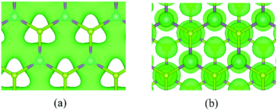
Recently, Lu et al.19 have succeeded in breaking the out-of-plane structural symmetry of single layer MoS2 forming MoSSe monolayers following a combination of chemical vapor deposition, H2 plasma stripping, and Se-selective thermal vaporization. Through this method, the general transition metal chalcogenide TMDs MX2 (M = Mo, W; X = O, S, Se, Te) can be changed into the Janus MXY counterpart with X ≠ Y as shown in Fig. 1.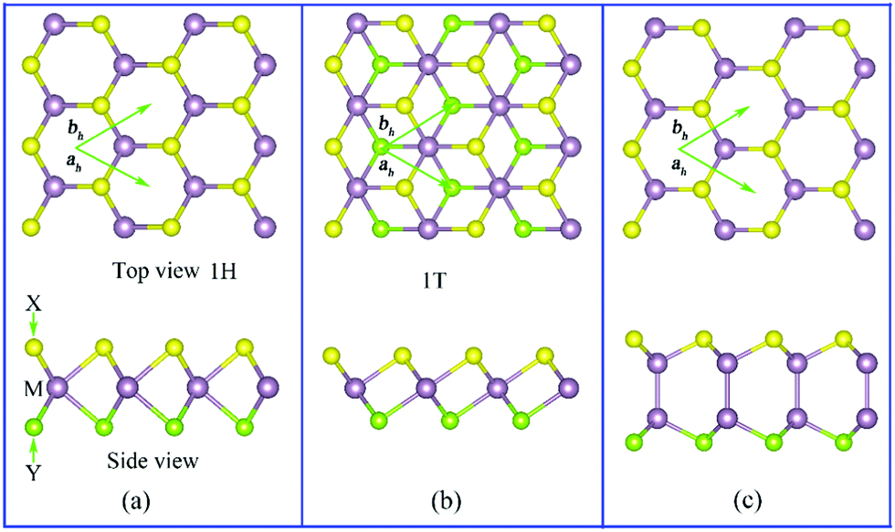 | ||
| Fig. 1 The atomic structure of different possible phases of low-dimensional Janus TMDs. (a) The 1-H phase of MXY monolayers. (b) The 1-T phase of MXY monolayers. (c) Group-III Janus M2XY or MM′XY monolayers (M, M′= Ga, In; X, Y= S, Se, Te). Top and side views of the Janus materials are shown in the upper and lower panels, respectively. The green arrows mark the primitive cell vectors (ah and bh). The X and Y atoms are shown in yellow and green, respectively. The M (M′) atoms are shown in mauve. | ||
Similar to graphene, also the single-layer transition metal chalcogenide MX2 has a hexagonal structure with P-6M2 (D3H-1) symmetry. However, unlike single-layer graphene, TMDs are made up of three distinct atomic layers arranged according to an X–M–X pattern. According to experimental and computational investigations, Janus TMDs (JTMDs) MXY can have different space groups. Some JMTDs as the 1-H and 1-T phases shown in Fig. 1(a) and (b) belong to the same P3M1 (C3V-1) group in spite of different atomic structures. In the 1-H phase, the X atom in the upper layer is right over the Y atom in the lower layer. Both the X and Y atoms are three-fold coordinated, while the M atom is six-fold coordinated. Conversely, the X or Y atoms in the 1-T phase are translated along the plane, which results in the X atom in the upper layer being located at the center of the hexagonal ring of the Y atoms. In the experiments, the 1-T phase can be obtained from high temperature treatment, and it is generally a metastable phase with respect to the 1-H phase.58
In addition to the aforementioned JTMDs, group-III mono-chalcogenides MX (M = Ga, In; X = O, S, Se, and Te) such as GaS can also have a hexagonal structure with symmetry group P3M1. Similar to TMDs, the X atoms are three-fold coordinated. However, the M-atom in the MX systems is four-fold (not six-fold) coordinated. To construct Janus structures out of monolayer MX compounds, the bottom X atoms need to be replaced by Y atoms, yielding M2XY (M = Ga, In; X, Y = O, S, Se, Te) monolayers (see in Fig. 1(c)). The Janus M2XY system can be further changed by substituting the M atoms with hetero-metal atoms (M′), forming MM′XY monolayers. In such a manner, Guo et al.59 generated a series of Janus monolayers, namely Ga2SSe, Ga2STe, Ga2SeTe, In2SSe, In2STe, In2SeTe, GaInS2, GaInSe2, and GaInTe2. These Janus structures can be further classified into two types: M2XY (M = Ga, In; X, Y = S, Se, Te) and MM′XY (M, M′= Ga, In; X, Y= S, Se, Te), both of which have broken inversion and mirror symmetries.
2.2 Possible low-dimensional structures
Starting from the phases for JTMDs presented in Section 2.1, several derivatives have been recently proposed and studied both experimentally and computationally. Many recent studies, which we review in the following, have reported on Janus nanotubes, nanoribbons, monolayers, multilayers, and hetero-structures in terms of both their stability and electronic properties.Mikkelsen et al.62 have recently investigated Janus MoSTe nanotubes by simulation. Starting from a 1-H monolayer of MoSTe, armchair and zigzag MoSTe nanotubes of different sizes were modeled. For both types of nanotubes, the simulations suggest promising signs of thermodynamic stability with respect to both their bulk constituents and their parent two-dimensional monolayer. The latter result is reported in Fig. 2(c), which displays the nanotube strain energy, defined as the energy difference with respect to the parent monolayer, as a function of the radius. Evidently, both the armchair and zigzag MoSTe nanotubes are stable with respect to their parent 2D layer with a strain-minimum at a radius of ∼18 Å. Furthermore, the authors also found that confinement effects were modest and that curvature leads to large changes in the band gap, with variations as large as 0.5 eV, and band-gaps both larger and smaller than for the pristine 2D MoSTe monolayer. Overall, these results suggest that Janus nanotubes can be thermodynamically stable, and that their electronic properties can be altered by controlling both their rolling type and curvature radius.
 | ||
| Fig. 2 (a) Sketch of the armchair and zigzag rolling directions for a planar, two-dimensional MoSTe monolayer, with the corresponding unit cells and Brillouin zones in the reciprocal space. (b) DFT-PBE calculated band structure of the MoSTe monolayer. The indirect band gap is marked by the blue arrow. (c) Calculated strain energies of the armchair and zigzag MoSTe nanotubes as a function of their radius. A minimum strain energy is attained at rmin, the radius of the most stable nanotube.62 | ||
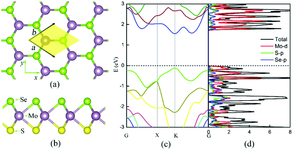 | ||
| Fig. 3 The atomic (a)–(b) and electronic (c)–(d) structures of the Janus MoSSe monolayer.25 (a) Top view of the MoSSe monolayer with the primitive cell highlighted by yellow shading. The marked x- and y-axes are parallel to the armchair and zigzag edges, respectively. (b) Side view of the MoSSe monolayer with the S, Mo and Se atoms lying on three different atomic layers (Mo: mauve, S: yellow, and Se: light green). The calculated band structure and (atom, angular-momentum resolved) density of states of the MoSSe monolayer are shown in panels (c) and (d), respectively. | ||
In addition to MoSSe, other Janus TMD monolayers have been proposed based on simulations. For example, Xia et al.66 studied the Janus WSSe monolayer using first-principles calculations. They found no negative frequency in the system's phonon dispersion, indicative of the dynamic stability for Janus WSSe monolayers. The characterization of the electronic structure of Janus WSSe reveals band gaps of about 1.70 eV (PBE) and 2.18 eV (HSE), slightly larger than that for the MoSSe monolayer at the same level of theory. Moreover, substitution of the Se atoms by Te atoms appears to reduce significantly the HSE calculated band gap from 2.18 eV (WSSe) to 1.71 eV (WSTe).
In addition to MoSSe and WSSe, other kinds of Group III Janus chalcogenide monolayer structures have been studied through simulations. Guo et al.59 focused on the following systems: Ga2SSe, Ga2STe, Ga2SeTe, In2SSe, In2STe, In2SeTe, GaInS2, GaInSe2, and GaInTe2. The authors found (PBE-DFT) band gaps in the range of 0.89–2.03 eV for these systems, uncovering appealing properties for applications in piezoelectric devices.
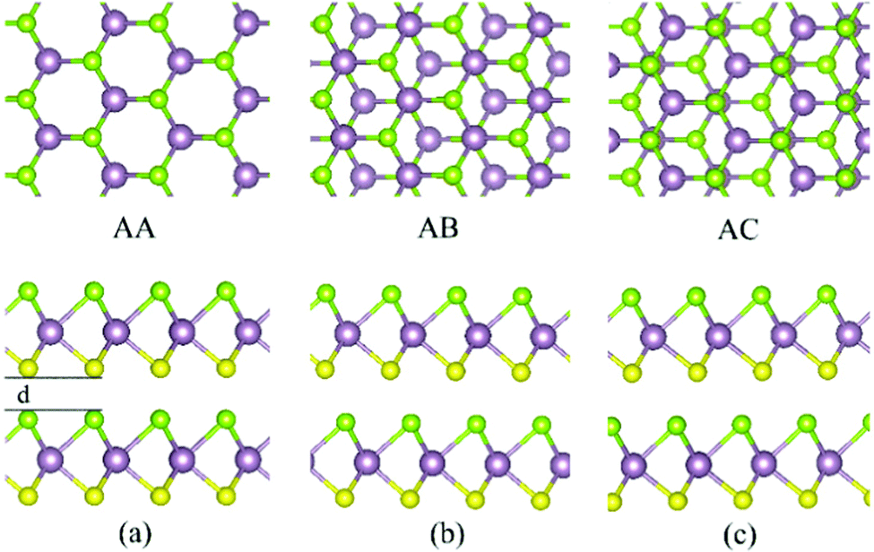 | ||
| Fig. 4 The different AA (a), AB (b) and AC (c) stacking types for the MoSSe bilayer. Top and side views are reported in the upper and lower panels, respectively. Same atom-color labeling as in Fig. 3. | ||
Li et al.71 explored different hetero-structures formed by combining MoSSe and WSSe Janus monolayers at a non-collinear PBE (PBE + SOC) level. They found that Rashba polarization is increased in vertical hetero-structures due to the increased out-of-plane electric polarity. As for the longitudinal heterostructures, consisting of two individual components stitched seamlessly within the 2D plane,71 their calculated photoresponse and absorption coefficients suggest optical activity in a wide visible-light range. Simulation of both classes of hetero-structures reveals type-II band alignment (staggered gap), where both the VBM and CBM of one component are a little higher than those of the other one, and accordingly favorable separation of excitons. Furthermore, Rawat et al.72 investigated a series of Janus hetero-structures formed by different kinds of Janus TMDs as MoXY/WXY (X, Y = S, Se, and Te). They found that depending on the composition and structure of the Janus TMD, the band gap can be tuned to a large extent from the infrared area to the ultraviolet region.72
In addition to hetero-structures consisting of two different Janus TMDs, research has also been carried out in other hetero-structures made up of Janus TMDs interfaced with other conventional two-dimensional materials. For instance, we investigated the hetero-structure formed by combining Janus MoSSe with nitride semiconductors, namely MoSSe/XN (X = Al, Ga).38 As the two sides of the Janus MoSSe monolayer are different, two different vertical hetero-structures can be formed (SeMoS/XN and SMoSe/XN) depending on whether the S- or Se-side of MoSSe faces the XN monolayer. Furthermore, owing to the in-plane structure of both MoSSe and XN, each vertical hetero-structure can be stacked in two different configurations (AA- and AB-) that are shown in Fig. 5. The simulations indicate that AB-[S-Ga] stacking results in the lowest formation energy (Ef = −0.266 eV) for SeMoS/GaN, which accordingly emerges as the energetically favored hetero-structure. The calculated band gaps vary from about 0.77 eV (SMoS/GaN, AA-[S-Ga]) to about 1.63 eV (SMoSe/GaN, AB-[Ga-Mo]), covering the near visible-infrared region. By changing the position of the S and Se atoms with respect to the GaN layer, the band gap can be further tuned to values from 0.77 to 1.47 eV that are still in the near visible-infrared region.
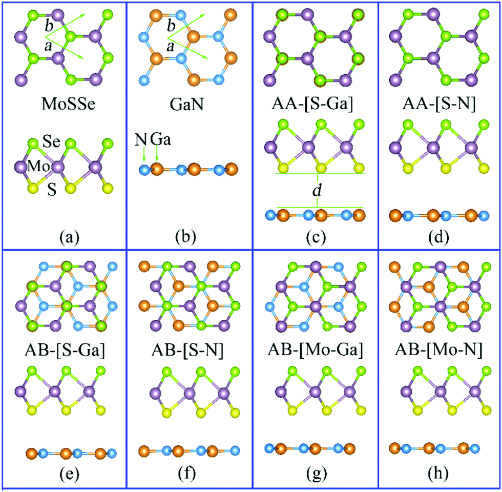 | ||
| Fig. 5 The atomic structure of the MoSSe (a) and GaN (b) monolayers, together with their AA (c)–(d) and AB stacked (e)–(h) SeMoS/GaN hetero-structures. The top and side views are shown in the upper and lower panels, respectively. The primitive cell is marked by the green arrows. The Mo, S, Se, Ga, and N atoms are shown as mauve, yellow, light green, orange, and blue spheres, respectively. The letter “d” denotes the interlayer distance between the top and bottom layers.38 | ||
Another interesting class of possible hetero-structure can be obtained by interfacing a Janus TMD monolayer with a zero-band gap semiconductor (semimetal) such as graphene. Recently, Vu et al.1 have investigated the WSeTe/graphene hetero-structure using first-principles calculations. They found that the electronic properties of both graphene and Janus WSeTe are well preserved in the WSeTe/graphene hetero-structure because of the weak vdW interactions. The optical absorption of the WSeTe/graphene hetero-structure is enhanced in both the visible and UV light regions with respect to that of the isolated graphene and Janus WSeTe monolayers. The absorption coefficient of the graphene/WSeTe hetero-structure for the visible light can reach 5 × 104 cm−1, which is two-times larger than that of the isolated Janus WSeTe monolayer. Zhao et al.73 studied the electronic properties of a Janus MoSSe sheet in contact with a zero-gap germanene electrode using first-principles calculations. The simulations indicate that the structural and electronic details of the two possible interfaces are markedly different depending on whether germanene faces the S- or Se-side of MoSSe. Notably, simulations of both kinds of interfaces suggest that in-plane tensile strain induces a transition from the Schottky to Ohmic behavior, and that increasing the thickness of MoSSe from monolayers to bilayers can lead to the formation of an Ohmic contact as a result of a zero Schottky barrier height.
The intrinsic dipole moment does not only adjust the Schottky barrier of the hetero-structure, but it also controls the charge carrier mobility and dynamics in the system. Liu et al.74 investigated by first principles calculations the electronic structures and dynamics of photo-generated carriers in Janus TMD (JTMDs) sheet and graphene in vdW sandwich heterojunctions (G/JTMDs/G) for photovoltaic cells. They found that the intrinsic built-in electric field in JTMDs results in an asymmetric potential, which can be used to enhance the separation and transfer of photo-generated carriers from JTMDs to different graphene layers. Owing to the built-in electric field in the G/JTMDs/G hetero-structure, such an enhanced separation is highly directional and takes place within hundreds of femtoseconds. Furthermore, the photo-generated electrons (holes) can be transferred from the MoSSe (MoSeTe) monolayer to the graphene sheets by the Se-side with a lower (higher) potential, while the recombination of holes (electrons) is suppressed due to the large separation between their final donor and acceptor states. The simulations also suggest that the graphene/WSeTe hetero-structure is characterized by an increased carrier mobility for both electrons and holes in comparison with an isolated graphene sheet. Of special relevance is the result that a band gap of about 10 meV at the Dirac cone of graphene can be opened in the hetero-structure. Depending on the stacking configuration, the graphene/WSeTe hetero-structure can form a p-type Ohmic or p-type Schottky contact with a small Schottky barrier of 0.35 eV. These results demonstrate that the intrinsic dipole moment and vertical strain can be effective in tuning both the contact type and the Schottky barrier height in hetero-structures made up of Janus TMDs and zero-gap semiconductors.
3. Properties
Unlike conventional MX2 TMDs, Janus MXY TMDs lack mirror symmetry, which introduces appealing properties such as large intrinsic electrostatic dipole moments perpendicular to the two-dimensional plane, tunable electronic band gaps as well as Rashba, excitonic and piezoelectric effects.75,76 As we review in the following, these properties make Janus low-dimensional materials appealing candidates for applications in very diverse fields such as field-effect transistors, electrocatalysis, photocatalysis, spintronics and piezoelectric devices.3.1 Basic electronic properties
Table 1 reports a compilation of the basic electronic properties for several low dimensional Janus MXY TMDs. Because of the different sizes and electronegativities of the X and Y atoms, the M–X and M–Y bond lengths and dipoles are inequivalent, resulting in the breaking of the mirror symmetry for Janus MXY monolayers. It is interesting to note that all the Janus MXY (M = Mo, W; X, Y = S, Se, Te) are semiconductors, regardless of the interface structure. Although the band gap of Janus monolayers depends on the stoichiometry of the system, atom-specific trends can be identified. For example, PBE results show that changing S into Te at the X or Y site of MoXY leads to a reduction of the band gap from 1.56 eV to 1.02 eV. Use of the HSE functional leads to an increase of the band gap up to about 0.5 eV by comparison with PBE results.| MXY | Method | a h (Å) | D M–X (Å) | E g (eV) | ΔU (eV) | D dip (e Å) | E b (eV) | Ref. |
|---|---|---|---|---|---|---|---|---|
| MoSTe Tube | PBE | 16.5 | 1.27 | 62 | ||||
| FeCl3I3 | DFT+U | 6.717 | 0.58 | 84 | ||||
| WSeTe | PBE | 3.45 | 2.56 | 1.42 | 0.68 | 52 | ||
| WSSe | HSE | 3.22 | 2.3 | 76 | ||||
| WSeTe | HSE | 3.38 | 1.75 | |||||
| MoSSe | HSE06 | 3.22 | 2.41 | 2.14 | 0.18 | 72 | ||
| MoSeTe | 3.4 | 2.55 | 1.70 | 0.21 | ||||
| MoSTe | 3.31 | 2.44 | 1.48 | 0.38 | ||||
| Ga2SSe | PBE | 3.72 | 2.04 | 85 | ||||
| AgBiP2Se6 | HSE06 | 6.696 | 2.25 | 0.27 | 0.28 | 0.63 | 86 | |
| WSSe | HSE | 3.26 | 2.42 | 2.13 | 0.73 | 0.23 | 87 | |
| MoSSe | GW | 3.25 | 2.42 | 2.569 | 88 | |||
| WSSe | GW | 3.28 | 2.42 | 2.68 | ||||
| InGaSTe | HSE06 | 3.91 | 2.63 | 2.32 | 0.74 | 0.27 | 82 | |
| In2SeTe | HSE06 | 4.18 | 2.78 | 1.85 | 0.27 | 0.12 | ||
| PtSSe | HSE + Soc | 3.63 | 2.43 | 2.14 | 0.75 | 0.23 | 83 | |
| PtSTe | 3.75 | 2.48 | 1.09 | 1.65 | 0.54 | |||
| PtSeTe | 3.81 | 2.57 | 1.04 | 0.92 | 0.31 | |||
| VSSe | DFT+U | 3.25 | 2.35 | 0.51 | 89 | |||
| WSSe | PBE | 3.247 | 1.4 | 0.738 | 90 | |||
| MoSSe Tube | PBE | 25.34 | 2.42 | 1.44 | 0.75 | 91 | ||
| MoSTe | HSE + Soc | 3.36 | 2.43 | 1.5 | 0.66 | 92 | ||
| PtSSe | HSE | 3.66 | 2.44 | 2.19 | 0.76 | 0.24 | 33 | |
| MoSSe | M-B | 2.66 | 0.85 | 93 | ||||
| SGaSe | HSE06 | 3.73 | 2.396 | 2.61 | 81 | |||
| SGaTe | 3.901 | 2.450 | 1.58 | |||||
| SeGaTe | 3.982 | 2.551 | 1.91 | |||||
| MoSSe | HSE06 | 3.25 | 2.42 | 2.02 | 79 | |||
| MoSSe | PBE | 3.250 | 1.528 | 1.56 (2.01) | 0.76 | 0.188 | 0.426 | 66 |
| MoSeTe | PBE (HSE) | 3.433 | 1.615 | 1.27 (1.71) | 0.74 | 0.198 | 0.469 | |
| MoSTe | 3.364 | 1.472 | 1.02 (1.47) | 1.47 | 0.383 | 0.447 | ||
| WSSe | 3.247 | 1.535 | 1.7 (2.18) | 0.72 | 0.174 | 0.347 | ||
| WSeTe | 3.432 | 1.623 | 1.35 (1.79) | 0.7 | 0.187 | 0.308 | ||
| WSTe | 3.361 | 1.478 | 1.23 (1.71) | 1.40 | 0.364 | 0.431 | ||
| MoSSe | PBE | 3.21 | 2.41 | 1.66 | 0.75 | 0.037 | 25 | |
| MoSSe T | HSE | 3.21 | 2.39 | 0.1 | 78 | |||
| In2SSe | GGA + Soc | 3.88 | 2.55 | 2.68 | 0.14 | 94 | ||
| MoOS | HSE06 | 3.01 | 2.05 | 1.55 | 2.3 | 0.48 | 32 | |
| MoOSe | 3.07 | 2.05 | 1.32 | 2.93 | 0.63 | |||
| MoOTe | 3.20 | 2.05 | 0.66 | 3.26 | 0.77 | |||
| Ga2S3 | HSE | 3.65 | 2.55 | 1.65 | 0.9 | 34 | ||
| Ga2Se3 | 3.84 | 1.68 | 1.3 | 0.69 | ||||
| Ga2Te3 | 4.16 | 0.77 | 0.88 | 0.63 | ||||
| TiSO | HSE06 | 3.175 | 1.27 | 95 | ||||
| TiSeO | 3.232 | 0.739 |
As the M-atom in Janus MXY monolayers is changed from Mo to W, the system's band gap is increased as a result of the larger atomic radius. This trend can be observed also for other metal atoms. For instance, in the dynamically, thermally and mechanically stable Janus MXY monolayers with M = Ti, Zr, and Hf, it is found that the band gap of the system changes from 0.74 to 2.88 eV with an increasing atomic radius for the M-atom.36
Further simulation work indicates that almost all the Janus SnXY monolayers are stable, with the exception of SnOTe. Apart from the case of Te-containing Janus materials, all the calculated band gaps vary with the X, Y-composition in the range of 0.33–1.74 eV, corresponding to the infra-red and near visible regions of the light-spectrum.77
Besides composition, the electronic properties of the MXY systems depend also on the specific phase (see also Fig. 1) as the band gap for the 1-T and 1-H phases can be profoundly different. It has been found that the 1-T phase of Janus MoSSe is a small band gap semiconductor and can even be computed to be a metal.78 Conversely, the 1-H phase of MoSSe is always a semiconductor with a large band gap of about 2.1 eV.79 In addition, the 1-H phase of the Janus WSeTe monolayer was proved to be a semiconductor with an indirect band gap of 1.1 eV, while the 1-T phase is semi-metallic (zero gap semiconductor). The two phases of WSeTe are separated by a small kinetic barrier of about 0.66 eV that needs to be overcome for the structural phase transition from 1-H to 1-T.80 In contrast to these cases, an extensive study of Janus group-III monochalcogenide M2XY (M = Ga, In; X, Y = S, Se, Te) monolayers indicates that all these systems are semiconductors with band gaps in the range of 0.89 eV to 2.03 eV.81,82 Overall, these results document the strong dependence on both the composition and phase for the band gap of Janus monolayers, reiterating the potential and prospects for function-tailored design of this class of materials.
Besides electronic band gaps, the compositional flexibility of Janus MXY monolayers can be used to tailor also the perpendicular electrostatic dipole moment and ensuing change of work-function (ΔU) between the two sides of the system. For example, the perpendicular dipole moment in MXY systems can change from 0.037 e Å (MoSSe) to 0.77 e Å (MoOTe).25,32 The occurrence of an intrinsic dipole moment in a semiconducting system implies an inherent electric field in the Janus materials perpendicular to the plane of the monolayer. This dipole moment can be further demonstrated from the inequality of the vacuum energy levels above either side of the monolayer. However, the ΔU of Janus PtSSe is about 0.75 eV83 and it increases to 1.65 eV for Janus PtSTe. ΔU can be further increased to 3.26 eV for Janus MoOTe.32 Besides substantial ΔU differences, the presence of an electrostatic dipole (and ensuing potential step) perpendicular to the plane of the system leads to peculiar localization of the valence and conduction band edges on different faces of the Janus MXY monolayer. It has been noted that such a potential difference can act as an auxiliary booster for photo-excited electrons, and also reduce the system's band gap to values smaller than 1.6 eV, as required for water splitting in the infrared region.35
3.2 Carrier mobility
Almost all of the low dimensional Janus materials synthetized or studied computationally to date are semiconductors, thence compatible with nanoscale photoelectric applications such as field effect transistors (FETs), electron-spin or piezoelectric devices, and photocatalysis. Charge carrier mobility is one of the most important factors controlling the performance in photoelectric applications, and several studies have focused on the nexus between this property and the composition (structure) of Janus low-dimensional materials. Table 2 reports a compilation of charge carrier mobility for different Janus low-dimensional materials.| Systems | Method | a h | η STH % | m e (mo) | m h (mo) | μ e (cm2 V−1 s−1) | μ h | Ref. |
|---|---|---|---|---|---|---|---|---|
| WSSe | HSE | 3.26 | 11.68 | 0.339 | 0.469 | 125.01 | 723.42 | 87 |
| MoSSe | GW | 3.25 | 0.47 | 0.59 | 72.21 | 163.52 | 88 | |
| WSSe | GW | 3.28 | 0.33 | 0.45 | 120.49 | 318.75 | ||
| InGaSTe | HSE06 | 3.91 | 10.6 | 0.17 | 1.54 | 3520 | 209 | 82 |
| In2SeTe | HSE06 | 4.18 | 18 | 0.22 | 5.13 | 3638 | 2735 | |
| PtSSe | HSE | 3.66 | 0.245 | 0.83 | 1546.52 | 671.92 | 33 | |
| MoSSe | HSE06 | 3.25 | 0.57 | 4.64 | 530 | 58 | 79 | |
| MoSSe | PBE | 3.25 | 0.51 | 0.55 | 65.82 | 246.19 | 66 | |
| MoSeTe | 3.433 | 0.64 | 0.72 | 37.25 | 108.44 | |||
| MoSTe | 3.364 | 0.47 | 1.65 | 78.53 | 24 | |||
| WSSe | 3.247 | 0.38 | 0.44 | 120.88 | 627.15 | |||
| WSeTe | 3.432 | 0.47 | 0.44 | 75.19 | 349.41 | |||
| WSTe | 3.361 | 0.48 | 1.53 | 129.91 | 48.84 | |||
| MoSSe | PBE | 3.21 | 0.60 | 0.73 | 73.8 | 157.2 | 25 | |
| 1T′-MoSSe | HSE | 3.21 | 0.13 | 0.17 | 1.21 × 10⁵ | 7.24 × 10⁴ | 78 | |
| Ga2S3 | HSE | 3.65 | 6.9 | 0.22 | 0.79 | 603.83 | 755.94 | 100 |
| Ga2Se3 | 3.84 | 28.4 | 0.16 | 0.3 | 1147.74 | 596.85 | ||
| Ga2Te3 | 4.16 | 46.2 | 0.45 | 0.23 | 8154.62 | 707.90 | ||
| TiSO 1T | HSE06 | 3.175 | 1.26 | 0.33 | 33 | 237 | 95 | |
| TiSeO | 3.232 | 1.323 | 0.253 | 38 | 539 | |||
| MoSSe/GaN | PBE | X | 0.55 | 0.65 | 263.28 | 3480.43 | 101 | |
| Y | 0.54 | 0.70 | 281.28 | 3951.21 | ||||
| WSeTe/WSTe | HSE06 | X | 19.91 | 0.54 | 1.71 | 221.54 | 278.32 | 72 |
| MoSSe/MoSSe | PBE | 3.21 | 0.57 | 0.7 | 1194 | 2915.6 | 25 |
It has been reported that the carrier mobility of electrons in MoS2 sheets is only about 200 cm2 V−1 s−1.96 To explore the effects of broken mirror symmetry on carrier mobility, we turned to the study of Janus MoSSe monolayers using first-principles calculations.25 The carrier mobility of electrons in the CBM along X-K is about 73.8 cm2 V−1 s−1, which is a little smaller than that of the MoS2 monolayer. The hole carrier mobility in the VBM along X–K is 157.2 cm2 V−1 s−1, about two times larger than for the electrons. Further results indicate that the thickness of the monolayer can significantly affect the carrier mobility in Janus MoSSe. Unexpectedly, we found that the carrier mobility of the electrons (1194 cm2 V−1 s−1) is about fifteen times larger than its monolayer case (73.8 cm2 V−1 s−1), while the hole carrier mobility is about twenty times larger (2915.6 cm2 V−1 s−1vs. 157.2 cm2 V−1 s−1 monolayer). To explore the dependence of carrier mobility on the thickness of the Janus system, we further modeled MoSSe bi- and trilayers in AC-stacking. Compared with the bilayer case (1194 cm2 V−1 s−1), the electron carrier mobility for the tri-layer decreases to 205 cm2 V−1 s−1, remaining however larger than for MoSSe (73.8 cm2 V−1 s−1) and MoS2 (160.6 cm2 V−1 s−1) monolayers. In contrast, the hole carrier mobility shows a completely different dependence on the system's thickness. The hole carrier mobility for the MoSSe tri-layer (5894 cm2 V−1 s−1) is about two times larger than that for the bilayer (2915.6 cm2 V−1 s−1). We chose few-layer MoSSe as the case system to clarify the higher carrier mobility of multilayer MoSSe by comparison with the single-layer case. The main determining factors can be disentangled as follows. First of all, the elastic moduli can be a main factor that affects the carrier mobility of the multilayer structure. This is because, in a phonon-limited approximation,97,98 the carrier mobility is directly proportional to the elastic modulus in the transport direction. When the structure contains more layers, it will be thicker, resulting in it being harder to stress or strain. Thus, the elastic moduli will increase with the layer number or thickness, leading to higher carrier mobility. Furthermore, it has been found that the carrier mobility of most few-layer structures is strongly sensitive also to the deformation potential, which in turn depends on the bonding characteristic and real space distribution of the valence band maximum (VBM) and conduction band minimum (CBM). For example, the bonding characteristics for the CBM and VBM in the monolayer and bilayer MoSSe are fundamentally different as shown in Fig. 6. For the monolayer case, the charge distribution is mainly in the x–y plane (see Fig. 6(a)), causing a larger change of charge distribution of the CBM than in the bilayer case, shown in Fig. 6(b). Thus, the structural deformation introduced along the x- or y-direction has a large effect on the bonding character of the CBM in the x–y plane, which leads to a relatively higher deformation potential (Ee) than in the bilayer case. Since, again in a phonon-limited approximation,97,98 the carrier mobility is inversely proportional to the square of the deformation potential, thicker layers will result in a smaller Ee, thence larger mobility.
 | ||
| Fig. 6 (a and b) The top view of the charge distribution in the CBM for monolayer (a) and bilayer (b) MoSSe. The isovalue for the surface plots is set at 0.01 e Bohr−3. | ||
In addition to MoSSe, several other Janus TMDs show interesting values and trends of their carrier mobility.99 For example, Fan et al.82 pointed out that the two dimensional Janus group-III chalcogenide multilayers InGaXY, M2XY and InGaX2 (M = In, Ga; X, Y = S, Se, Te) have promising high carrier mobility. This study found that the electron and hole carrier mobility in In2SeTe can be as high as about 3638 and 2735 cm2 V−1 s−1, respectively Recently, we also considered the effect of vdW interactions, as present in MoSSe/GaN hetero-structures, on charge carrier mobility using first-principles calculations. Simulation of these systems suggests appealingly high mobilities of 281.28 cm2 V−1 s−1 and 3951.2 cm2 V−1 s−1 for the electrons and holes, respectively. Overall, these results lead to the conclusion that the carrier mobility in Janus structures can be significantly adjusted by altering the composition, thickness, and interlayer interactions of the system.
3.3 Schottky barriers
Besides carrier mobility, several other parameters such as the type of electric contact, the presence of rectifying (Schottky) barriers and ensuing on/off ratio are crucial for the performance of a material in photoelectric applications. Generally, it is difficult to achieve a hetero-structure with multifunction in one structure without any other external interaction. The tunable intrinsic electrostatic dipole moment and interfacing geometry in Janus hetero-structures make this class of materials potentially appealing for photoelectric applications. Table 3 presents a compilation of structural and electronic properties for different Janus hetero-structures that have been recently considered in the literature.| Systems | Method | XY | E b (meV Å−2) | D (Å) | E g (eV) | E sb (eV) | ΔU (eV) | E dip (e Å) | μ STH (%) | Ref. |
|---|---|---|---|---|---|---|---|---|---|---|
| MoSSe/Germanene | PBE | X | 191.37 meV | 2.92 | 0.025 | 0.3 n | 0.8 | 73 | ||
| Y | 186.61 | 3.07 | 0.041 | 1.25 p | 1.2 | |||||
| MoSSe/GaN | PBE | X | −0.266 eV | 2.943 | 0.89 | 101 | ||||
| Y | −0.255 | 3.107 | 1.45 | |||||||
| WSeTe/Gr | PBE | X | −16.51 | 3.4 | 0.01 | 0.35 p | 0 | 52 | ||
| Y | −15.08 | 3.54 | 0.008 | 0 | 0 | |||||
| WSeTe/WSTe | HSE06 | X | −0.027 | 3.25 | 1.71 | 19.91 | 72 | |||
| Ga2SSe/Gr | PBE | X | −50.32 | 3.42 | 0.015 | 0.76 n | 85 | |||
| Y | −51.35 | 3.40 | 0.017 | 0.76 n | ||||||
| Gr/MoSSe/Gr | HSE | 3.42 | 0.14 | 0.42 n | 74 | |||||
| 3.51 | ||||||||||
| MoSSe/ZnO | HSE | X | −0.399 | 3.29 | 2.0 | 1.18 | 102 | |||
| Y | −0.448 | 3.41 | 2.1 | 1.07 | ||||||
| WSSe/ZnO | X | −0.541 | 3.31 | 2.1 | 1.27 | |||||
| Y | −0.392 | 3.37 | 2.3 | 1.07 | ||||||
| InGaSTe/InGaSTe | HSE06 | −18.92 | 4.15 | 1.68 | 1.43 | 0.52 | 28.5 | 82 | ||
| In2SeTe/In2SeTe | −19.48 | 4.19 | 1.32 | 0.61 | 0.24 | 33.7 | ||||
| MoSSe/SiC | PBE | −21.1 | 3.404 | 1.117 | 5.748 | 103 | ||||
| WSSe/SiC | −15.1 | 3.612 | 1.426 | 5.849 | ||||||
| MoSSe/AlN | PBE | X | −0.3 | 2.71 | 1.25 | 1.27 | 0.051 | 38 | ||
| Y | −0.27 | 2.96 | 1.68 | 0.1 | 0.018 | |||||
| MoSSe/GaN | X | −0.26 | 2.97 | 0.8 | 1.3 | 0.053 | ||||
| Y | −0.25 | 3.12 | 1.45 | 0.24 | 0.022 | |||||
| PtSSe/PtSSe | 2.65 | 2.09 | 0.65 | 1.21 | 33 | |||||
| MoSSe/MoSSe | PBE | 3.14 | 0.8 | 104 | ||||||
| PtSSe/Gr | PBE + soc | X | −2.482 | 3.32 | 0.16 | 0.094 n | 0.143 | 105 | ||
| Y | −2.474 | 3.408 | 0 | 0.449 n | 1.062 | |||||
| MoSSe/TGCN | HSE06 | X | −31 | 3.35 | 2.15 | 0.62 | 106 | |||
| Y | −30 | 3.45 | 2.15 | 0.98 | ||||||
| MoSTe/TGCN | HSE06 | X | −12 | 3.31 | 1.73 | 1.54 | 0.44 | |||
| Y | −11 | 3.61 | 1.73 | 1.95 | 0.44 | |||||
| MoSSe/MoSSe | PBE | −0.312 | 2.909 | 0.96 | 0.063 | 25 | ||||
| MoSSe/WSSe | G0W0 | 3.06 | 1.83 | 71 |
As shown in Table 3, the band gap of Janus hetero-structure can be significantly altered as a function of both the composition and interfacing mode of the system. For instance, the band gap of the whole hetero-structure can be changed substantially from 0 eV for WSeTe/Graphene52 to 2.3 eV for WSSe/ZnO.102 To sustain the development of this class of materials for photoelectric applications, in addition to the band gap, it is essential to know the type (p-, n-, and p–n) and Schottky barriers present in the Janus hetero-structure. Vu et al.52 studied the graphene/WSeTe hetero-structure using first-principles calculations. Their results show that p-type Ohmic contact or p-type Schottky contact with a small Schottky barrier of 0.35 eV can exist in this Janus hetero-structure. Further results suggest that vertical electric fields and strain can be used to change the contact types and Schottky barriers in graphene/WSeTe hetero-structures from p-type to n-type Schottky contacts, or to p-type Ohmic contacts. Research in this class of compounds includes also the work by Zhao et al. who modeled using first principles calculations the electronic properties of Janus MoSSe in contact with germanene, a zero-gap material. The results show that the contact characteristics are significantly different, since SeMoS/Ge and SMoSe/Ge are n-type and p-type, respectively. Notably, for both types of MoSSe/germane interfacing, in-plane tensile strain induces a transition from Schottky to Ohmic behavior.73 Overall, these results indicate that, in contrast to conventional hetero-structures, the Janus ones offer control of the Schottky barrier via modulation of the intrinsic electrostatic dipole moment in the system.
3.4 Excitonic effects
When the structure of a material changes from three-dimensional to two-dimensional with finite thickness, excitonic effects tend to increase due to the reduced dimensionality and ensuing weakening of dielectric screening.88 These considerations have prompted interest in excitonic effects for low dimensional Janus materials. From the experimental side, Zheng et al.107 used absorbance and photoluminescence spectroscopy to investigate room-temperature exciton resonances for Janus MoSSe and WSSe monolayers. Transient absorption measurements reveal that excitons in Janus structures form about 30% faster than in pristine TMDs as a result of enhanced electron–phonon interactions due to the built-in electrostatic dipole moment. Combining the steady-state photoluminescence quantum yield and time-resolved transient absorption measurements, the authors further found that exciton radiative recombination lifetimes in Janus structures are significantly longer than in their pristine (MoS2) samples. These measurements support the predicted spatial separation of the electron and hole wave functions due to the built-in dipole moment. From the theoretical side, Xia et al.66 used first-principles calculations to explore the electronic properties of Janus MXY (M =Mo, W; X, Y = S, Se, Te) monolayers for photocatalytic applications. The authors found that the exciton binding energy for these Janus materials ranges from ∼0.31 eV to ∼0.47 eV. In addition, Fu et al.100 found that excitonic effects are more pronounced in Group III metal dichalcogenides than in Janus TMDs, with the calculated exciton binding energies ranging from about 0.63 eV (Ga2S3) to 0.9 eV (Ga2Te3). Additional recent results indicate that the exciton binding energy can be further adjusted by the formation of Janus hetero-structures and engineering of the interfaces therein,71,93 which prompts for further research efforts in the understanding and control of excitonic effects in Janus-systems for photocatalytic applications.3.5 Rashba effects
Generally, it is difficult to find Rashba spin splitting in perfect TMDs due to the out-of-plane mirror symmetry and the ensuing absence of perpendicular electrostatic dipoles and potential steps.21 However, since the successful preparation of Janus MoSSe with both in-plane inversion and breaking of the out-of-plane mirror-symmetry, the interest in Rashba-type spin-splitting in Janus 2D systems has been steadily growing. Hu et al.108 systematically investigated the effects of perpendicular external electric fields and in-plane biaxial strain on the Rashba spin-splitting of a series of Janus MXY monolayers (M = Mo, W; X, Y = S, Se, Te) using first-principles calculations. They found that the Zeeman-type spin-splitting and valley polarization at the K (K−) point are well preserved regardless of the applied field and strain. The authors also observed a Rashba-type spin-splitting around the Γ point for all the MXY systems. Li et al.71 investigated computationally vertical hetero-structures (VHTs) and lateral hetero-structures (LHTs) made up of Janus MoSSe and WSSe monolayers. They found that the Rashba polarization can be enhanced in VHTs due to the enhanced out-of-plane electrostatic polarity. Other methods can be also used to manipulate the Rashba effect. Chen et al.109 explored using first-principles calculations the use of charge doping as a strategy to manipulate the Rashba effect in 2D Janus TMDs. The authors found that electron doping can strengthen the Rashba spin splitting at the valence band maximum (VBM) and conduction band minimum (CBM) of 2D Janus TMDs without constant energy consumption, as required by traditional techniques (electric fields and strain engineering). However, the authors also found that hole doping weakens Rashba effects in 2D Janus TMDs. Overall, these results indicate that Rashba effects, a prominent characteristic of the Janus TMDs, are amenable to tuning by nanostructuring and doping strategies as well as by more traditional approaches such as strain or gating.The Rashba effect can be used to design different spintronic devices for future applications. According to their specific function, the spintronic devices can be classified into spin field effect transistors, spin interference devices, nonmagnetic spin filters, photodetectors, and so on. For example, Yusoff et al.110 studied compositionally engineered perovskite single crystals by relativistic first-principles calculations, and found a large Rashba splitting of about 117 meV. Owing to this large Rashba effect, significant spin-momentum locking can be achieved, resulting in a hybrid perovskite single crystal photodetector with a detectivity of more than 1.3 × 10¹⁸ Jones (cm Hz1/2 W−1). In addition, Din et al.53 investigated the geometry and electronic properties of vdW heterostructures GeC/MSSe (M = Mo, W) by performing first-principles calculations. It was found that Rashba spin polarization in GeC/WSSe is larger than in GeC/MoSSe due to the larger SOC effect for the heavier W atoms by comparison with the lighter Mo ones. These results point to the GeC/WSSe heterostructures as a preferential platform for experimental and theoretical development of two-dimensional spintronic devices. On the other hand, Nitta et al.111 studied the Rashba spin–orbit interaction in InGaAs quantum wells by the weak antilocalization analysis method. The authors observed a clear cross-over from positive to negative magnetoresistance near zero-magnetic field by controlling the degree of the structural inversion asymmetry, identifying a zero-field spin-splitting induced by the Rashba effect. Such a spin-splitting was identified to result in a spin-filter device based on the Rashba effect using a nonmagnetic resonant tunneling diode structure. Further calculations on the InAIAs/InGaAs heterostructures show that the spin-filtering efficiency can exceed 99.9%.
To conclude this section, recent work in the field clearly demonstrates that Janus TMDs, by comparison with their standard TMD-analogues, have unique and tunable properties such as electronic band gaps, carrier mobility, and Schottky barriers in addition to notable Rashba, excitonic and piezoelectric effects. Importantly, all these properties turn out to be amenable to tailoring by controlling the intrinsic electrostatic dipole moment in the hetero-structures as determined by the composition, thickness, and intimate interface geometry of the composite system.
4. Potential applications
The discovery of Janus MoSSe monolayers has attracted extensive attention for a wide range of applications. It has been suggested that the properties of Janus materials make them promising candidates for photocatalytic water splitting, hydrogen evolution reduction, spintronics, piezoelectric devices, and so on. In this section, we review the range of potential applications that have started to be explored in the literature over the recent years.4.1 Photocatalytic water splitting
For an efficient photocatalytic water splitting, the photocatalyst should have a suitable band gap, band edge position, and effective carrier mobility. Owing to their large surface area, tunable band gaps and band edge positions for optimal redox potentials, various Janus materials have been suggested as promising photocatalysts for water splitting.81,112,113 Ma et al.79 explored using first-principles calculations the potential of Janus MoSSe monolayers for water-splitting photocatalysis, also under application of isotropic and uniaxial strains. They found that Janus MoSSe monolayers exhibit pronounced visible-light absorption efficiency, and that they have valence and conduction band edges suitable for initializing the redox reactions of H2O as well as high carrier mobility. H2O molecules adsorb more strongly on the MoSSe monolayer surfaces than on MoS2, which is beneficial for water-splitting reactions. In addition, thickness-effects can also be used to tune the properties of Janus materials for water splitting. First principles simulations by Guan et al.31 suggest that Janus MoSSe multilayers can exhibit excellent visible light water splitting performance. Besides MoSSe, a variety of Janus 2D materials, such as Janus MoXY (X, Y = O, S, Se, and Te),32 PtSSe,21 and XM2Y (X, Y = S, Se, Te; M = Ga, In)100 monolayers have been systematically investigated using first principles simulations in terms of their photocatalytic activity. This work focused on electronic structures and band gaps, redox potentials, interactions with water molecules and carrier separation processes, leading to the suggestion that these Janus 2D materials could be efficient photocatalysts for water splitting. Recently, we found that also Janus hetero-structures can be appealing systems for effective water splitting. Focusing on Janus MoSSe and nitrides XN (X = Al, Ga) hetero-structures, we investigated the structural and electronic properties of these systems using first-principles calculations.38 The simulations show that the MoSSe/AlN hetero-structures have indirect band gaps in the range of 1.00–1.68 eV. Conversely, the MoSSe/GaN hetero-structures are direct-gap semiconductors with band gaps of 0.8–1.51 eV. Interestingly, although the band gap of the MoSSe/XN hetero-structures can be smaller than 1.23 eV, the band edge positions turn out to be suitable for photocatalytic water splitting in the visible-infrared region of the spectrum (Fig. 7). This peculiar behavior originates primarily from the intrinsic electrostatic dipole of the system, leading to an electrostatic potential difference between the two sides of the system as well as VBM and CBM distributed on opposite sides of the hetero-structure. This electrostatic potential difference, besides acting as an auxiliary booster for separation and diffusion of photo-induced carriers, is also effective in reducing the band gap required for water splitting in the visible-infrared region. Overall, these results suggest that engineering of the intrinsic dipole moment of Janus materials can be highly effective in regulating the activity and performance of the system for water splitting.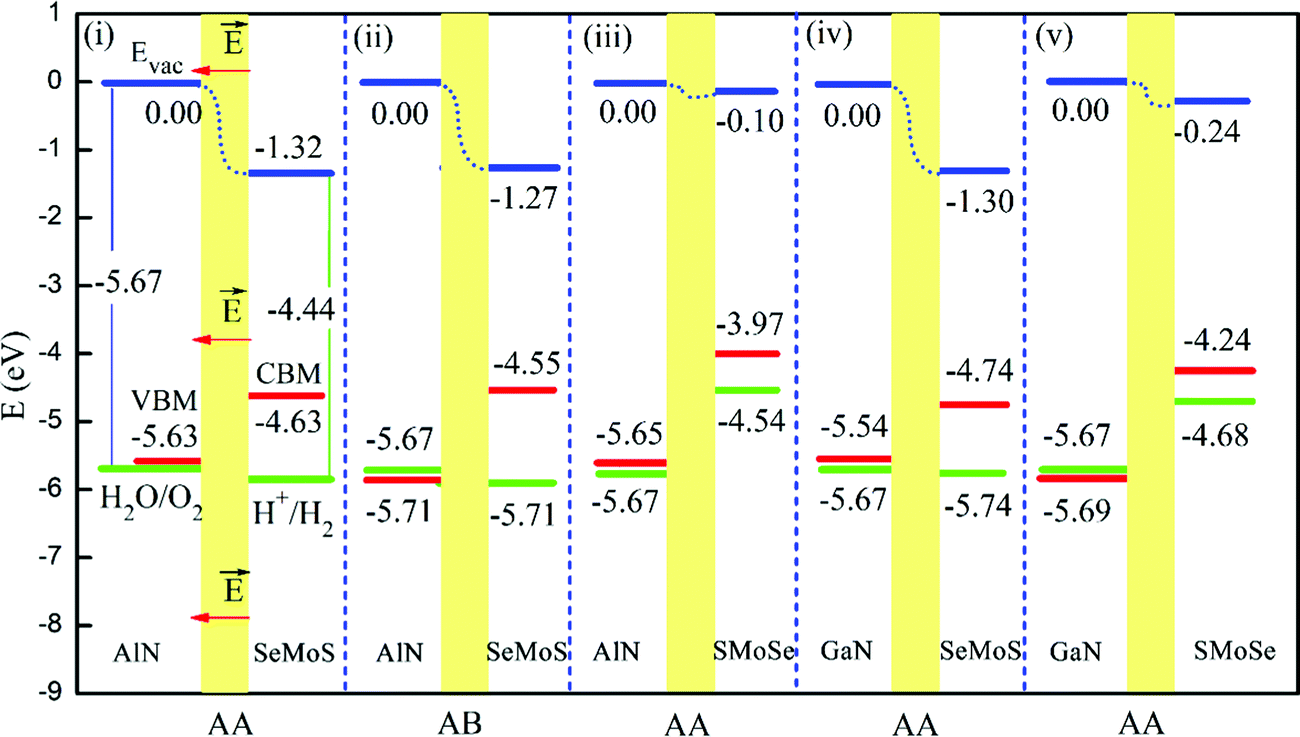 | ||
| Fig. 7 The position of the valence Band (VBM, left red horizontal lines) and conduction Band (CBM, right red lines) edges for different Janus MoSSe/XN hetero-structures, after alignment to the vacuum energy levels (blue lines), together with the standard oxidation (left green lines) and reduction (right green lines) potentials of water. The red arrows mark the direction of the intrinsic electric field across the interfacial region (yellow shading) of the MoSSe/XN hetero-structures.38 | ||
4.2 Hydrogen evolution reaction (HER)
Because of the compositional flexibility and ensuing high tunability of electronic properties, Janus TMD materials have been regarded as promising catalysts also for the hydrogen evolution reaction (HER). It has been reported that the excellent catalytic activity of TMDs can be mainly attributed to vacancies, edge sites, doping, impurities, and grain boundaries.29,114,115 Er et al.50 found that the recently synthesized family of Janus TMDs can be promising candidates for the HER due to the inherent structural asymmetry. They specifically identified the Janus WSSe monolayer as a promising candidate since its basal plane can be activated without large applied tensile strains and in the absence of a significant density of vacancies. Furthermore, the simulations also suggest that it may be possible to realize a strain-free Janus TMD-based catalyst with intrinsic high HER catalytic performance. The calculated density of states and electronic structure reveal the introduction of in-gap states and a shift of the Fermi level following hydrogen adsorption. These effects are due to the Janus asymmetry and have been suggested as indicative of enhanced HER activity.Further research in the field has focused on the role of defects in Janus TMDs for the HER activity. Shi et al.116 used density functional theory to study all of the possible intrinsic defects on the MoSSe monolayer and their effects on the HER. The simulations suggest that the Janus MoSSe monolayer with different grain boundaries, vacancies (VS, VSe, VSSe, VMo, and VMoS3), and antisite defects (MoSSe, SeMo, and SMo) shows enhanced HER performance. The details of hydrogen adsorption at the defect-sites were rationalized by using a “states filling” model. The hydrogen adsorption energy during the catalytic process changes linearly with the energy required to fill unoccupied electronic states within the catalysts. Based on the above research, Hao et al. explored and optimized in silico the HER activity by changing the X atoms in Janus 1T-MoSX (X = O, Se, and Te). The introduction of 1T-MoSO was found to yield the optimal adsorption energy for hydrogen adatoms.117 These investigations have advanced substantially the current understanding of the catalytic activity of Janus TMDs for the HER, paving the way for future work in the development of high-performance HER catalysts based on this class of materials.
4.3 Piezoelectric devices
The piezoelectric properties of low-dimensional materials have received growing attention due to their potential applications in nanoscale energy harvesting, sensors, and actuators. Unfortunately, in all of the systems studied to date, strain and electric polarization are confined to the basal plane, which limits the practical integration of these materials in piezoelectric devices. Dong et al.118 investigated recently synthesized Janus MXY (M = Mo, W; X, Y = S, Se, Te) monolayers and multilayer structures using first-principles calculations. They found that large out-of-plane piezoelectric polarization exists in these materials. For monolayer structures, both strong in-plane and much weaker out-of-plane piezoelectric polarizations can be induced by uniaxial strain in the basal plane. For the multilayer cases, an extremely strong out-of-plane piezoelectric polarization can be obtained as the strain can be transferred to the basal plane, regardless of the stacking sequence. The out-of-plane piezoelectric coefficient d33 of multilayer MoSTe can reach 5.7–13.5 pm V−1 depending on the stacking sequence. This is much larger than that for the commonly used 3D piezoelectric material AlN (d33 = 5.6 pm V−1). Similarly, Cai et al.69 also considered the thickness effect in studying Janus MXY bilayers (M = Mo, W; X, Y = S, Se, Te) using first-principles calculations. They found that in-plane interlayer sliding of Janus MXY bilayers can lead to significant enhancement of its vertical piezoelectricity. The tribo-piezoelectric transduction mechanism is elucidated by the tribological energy conversion of Janus TMD bilayers overcoming the interlayer sliding resistance to reach the AA-stacking states and resulting in the strongest out-of-plane piezoelectricity. To understand the phase effect, Yagmurcukardes et al.92 investigated the electronic, and piezoelectric properties of two dynamically stable crystal phases of monolayer Janus MoSTe (1H and 1T phase) using first-principles calculations. Systematic analysis of the piezoelectric stress and strain coefficients indicates that out-of-plane piezoelectricity appears in the 1H phase and that the non-central symmetric 1T phase has large piezoelectric coefficients. Other Janus TMD materials have also been proposed from theoretical predictions. Chen et al.19 have proposed a new family of 2D nanomaterials, Janus transition metal oxides and chalcogenide MXY (M = Ti, Zr, Hf; X, Y = O, S, Se) monolayers, for nanoelectronics and piezoelectric applications. They found that TiSO, ZrSO, and ZrSeO monolayers possess large piezoelectric properties because of the broken inversion symmetry due to the different atomic sizes and electronegativities of the X and Y elements. Such piezoelectric properties are better than or comparable to those of other 2D and bulk piezoelectric materials. Besides Janus TMDs, Guo et al.59 investigated the group-III monochalcogenide monolayers including Ga2SSe, Ga2STe, Ga2SeTe, In2SSe, In2STe, In2SeTe, GaInS2, GaInSe2, and GaInTe2 by computation. The simulation results show that these Janus structures possess piezoelectric coefficients up to 8.47 pm V−1, over four times the maximum value relative to the GaS2 monolayer. Moreover, the broken mirror symmetry of these Janus structures induces out-of-plane dipolar polarization, yielding additional out-of-plane piezoelectric coefficients of 0.07–0.46 pm V−1. Therefore, Janus materials can generate out-of-plane piezoelectric coefficients, and the piezoelectric properties can be changed by the different Janus structures, phases, thicknesses, and so on.4.4 Gas sensing devices
Conventional two dimensional TMDs have been long identified as appealing materials for high-performance gas sensing,119 which has motivated recent interest in the adsorption of several molecules on Janus TMDs, in particular Janus MoSSe.120Table 4 reports a compilation of the main results of recent research in sensing of gas molecules adsorbed on low dimensional Janus materials. It should be mentioned that the adsorption energy is negative, thus lower values of adsorption energy indicate stronger adsorption. Interestingly, due to the asymmetric structure and the associated built-in electrostatic dipole and electric field, the interactions between adsorbed molecules such as CO, CO2, NH3, NO and NO2 on Janus MoSSe monolayers are stronger than those on MoS2 monolayers. Taking NO2 as an example, the adsorption energy of NO2 on MoS2 is about −0.21 eV, while it can be lowered to −0.24 eV on MoSSe.120 Furthermore, adsorption on the Se-side of Janus MoSSe is much stronger than on the S-side. Application of uniaxial tensile strain leads to further enhancement of the adsorption strength of NH3 and NO2 on the Se-side of Janus MoSSe monolayers. The adsorption strength can be further enhanced by surface defects and edge modification. For example, the adsorption energy of molecular H2O on a perfect Janus MoSSe sheet is about −0.243 eV. However, the adsorption energy can be increased to −0.321 eV if H2O adsorbs on the S-vacancy site.121 This tendency can be found also for NO, NO2 or other molecules, suggesting a critical role for Se and S/Se vacancies in controlling the sensitivity of MoSSe for molecular adsorption and related gas-sensing applications.| Substrate | Molecule | B l (Å) | E a (eV) | M (μB) | Ref. |
|---|---|---|---|---|---|
| MoSSe | H2O | 2.66 | −0.243 | 0 | 121 |
| MoSSe-VS | H2O | 2.985 | −0.321 | 0 | |
| MoSSe | CH3OH | −0.25 | 122 | ||
| MoSSe-edge | N2 | −1.43 | 0 | 37 | |
| MoSSe-S side | CO | 3.15 | −0.13 | 0 | 120 |
| CO2 | 3.06 | −0.18 | 0 | ||
| NH3 | 2.67 | −0.19 | 0 | ||
| NO | 2.77 | −0.14 | 0 | ||
| NO2 | 2.78 | −0.22 | 0 | ||
| MoSSe | |||||
| VSSe | H2S | 1.609 | −0.238 | 0 | 123 |
| VSe | NH3 | 0.876 | −0.281 | 0 | |
| VSe | NO2 | 1.776 | −3.36 | 1.0 | |
| VSSe | NO | 0 | −2.894 | 1.01 |
5. Conclusions and outlook
Owing to their peculiar properties by comparison with conventional two dimensional materials, Janus TMDs have attracted considerable interest from researchers working in different fields. The removal of mirror symmetry in Janus materials brings about unique properties, which make these systems promising for a variety of applications. This review has focused mainly on recent theoretical and computational advances in understanding and controlling these properties, with special focus on possible competing structural phases, emerging properties, and potential applications for low dimensional Janus materials. Based on the theoretical results reviewed, low dimensional Janus TMDs exhibit very peculiar properties such as intrinsic out-of-plane dipole moments, tunable band gap, strong Rashba spin-splitting, sizable carrier mobility, and relatively strong excitonic effects. These properties in turn suggest potential for diversified applications ranging from nanoscale electronics to optoelectronics, to photocatalytic water splitting and piezoelectric devices.To date, only the Janus MoSSe and WSSe monolayers have been successfully synthesized by selenization of monolayer MoS2 and sulfurization of monolayer WSe2, respectively. As a result, most of the recent research on Janus low dimensional materials has been of theoretical and computational nature. This suboptimal situation prompts for continued and increased efforts in the preparation and characterization of Janus two dimensional materials and related hetero-structures, towards realization of the full potential of this class of materials for technological applications.
From a theoretical and computational perspective, most of the simulations of Janus TMD materials so far have focused on systems under vacuum conditions. However, the viable use of Janus TMDs for photocatalytic water splitting, the hydrogen evolution reaction, gas sensing, piezoelectric devices and other practical applications requires these materials to be exposed to different gas, liquid and solid environments. It is thus necessary to extend research in this field by studying the performance of these materials under realistic conditions i.e., by considering also their surrounding medium and operating conditions.
Last but not least, although recent simulation results indicate that excitonic effects are dramatically increased in Janus low dimensional materials, quantitative understanding of the behavior of excess charge, possible polaron formation and exciton dynamics is yet to be reached and should be prioritized in the near-future. This is necessary to understand not only the individual systems but also the charge and energy transfer processes in multi-layered hetero-structures.
Conflicts of interest
There are no conflicts to declare.Acknowledgements
This work was supported by the Science Challenge Project (TZ2018004), the National Natural Science Foundation of China (No. 51572016, U1530401, 11704116, 11804090, 51472209, 11774298, U1401241, 11974037, and 21503012), and the Natural Science Foundation of Hunan Province, China (Grant No. 2019JJ50175 and 2019JJ50148). This research was also supported by a Tianhe-2JK computing time award at the Beijing Computational Science Research Center (CSRC). G. T. and L.-M. L. acknowledge support from the Royal Society Newton Advanced Fellowship scheme (Grant No. NAF\R1\180242).References
- K. S. Novoselov, A. K. Geim, S. V. Morozov, D. Jiang, Y. Zhang, S. V. Dubonos, I. V. Grigorieva and A. A. Firsov, Science, 2004, 306, 666 CrossRef CAS PubMed.
- T. Fang, A. Konar, H. Xing and D. Jena, Phys. Rev. B: Condens. Matter Mater. Phys., 2008, 78, 205403 CrossRef.
- A. Betti, G. Fiori and G. Iannaccone, Appl. Phys. Lett., 2011, 98, 212111 CrossRef.
- M.-Q. Long, L. Tang, D. Wang, L. Wang and Z. Shuai, J. Am. Chem. Soc., 2009, 131, 17728 CrossRef CAS PubMed.
- X. Wang, Y. Ouyang, X. Li, H. Wang, J. Guo and H. Dai, Phys. Rev. Lett., 2008, 100, 206803 CrossRef PubMed.
- H. C. Yang, Y. Xie, J. Hou, A. K. Cheetham, V. Chen and S. B. Darling, Adv. Mater., 2018, 30, e1801495 CrossRef PubMed.
- Y. Gong, et al. , Nat. Nanotechnol., 2018, 13, 294 CrossRef CAS PubMed.
- H. Zhang, Y.-N. Zhang, H. Liu and L.-M. Liu, J. Mater. Chem. A, 2014, 2, 15389 RSC.
- M. Chhowalla, H. S. Shin, G. Eda, L.-J. Li, K. P. Loh and H. Zhang, Nat. Chem., 2013, 5, 263 CrossRef PubMed.
- C. Ataca, H. Şahin and S. Ciraci, J. Phys. Chem. C, 2012, 116, 8983 CrossRef CAS.
- Q. Xiang, J. Yu and M. Jaroniec, J. Am. Chem. Soc., 2012, 134, 6575 CrossRef CAS PubMed.
- B. Radisavljevic and A. Kis, Nat. Mater., 2013, 12, 815 CrossRef CAS PubMed.
- T. Jin, J. Kang, E. Su Kim, S. Lee and C. Lee, J. Appl. Phys., 2013, 114, 164509 CrossRef.
- L. Ju, M. Bie, X. Zhang, X. Chen and L. Kou, Front. Phys., 2020, 16, 13201 CrossRef.
- S. Najmaei, et al. , Nat. Mater., 2013, 12, 754 CrossRef CAS PubMed.
- N. Huo, Y. Yang, Y.-N. Wu, X.-G. Zhang, S. T. Pantelides and G. Konstantatos, Nanoscale, 2018, 10, 15071 RSC.
- Y. Cai, G. Zhang and Y.-W. Zhang, J. Am. Chem. Soc., 2014, 136, 6269 CrossRef CAS PubMed.
- Y. C. Cheng, Z. Y. Zhu, M. Tahir and U. Schwingenschlögl, Europhys. Lett., 2013, 102, 57001 CrossRef.
- A.-Y. Lu, et al. , Nat. Nanotechnol., 2017, 12, 744 CrossRef CAS PubMed.
- J. Zhang, et al. , ACS Nano, 2017, 11, 8192 CrossRef CAS PubMed.
- R. Peng, Y. Ma, S. Zhang, B. Huang and Y. Dai, J. Phys. Chem. Lett., 2018, 9, 3612 CrossRef CAS PubMed.
- W. Chen, E. J. Santos, W. Zhu, E. Kaxiras and Z. Zhang, Nano Lett., 2013, 13, 509 CrossRef CAS PubMed.
- K. F. Mak, C. Lee, J. Hone, J. Shan and T. F. Heinz, Phys. Rev. Lett., 2010, 105, 136805 CrossRef PubMed.
- S. Cahangirov, C. Ataca, M. Topsakal, H. Sahin and S. Ciraci, Phys. Rev. Lett., 2012, 108, 126103 CrossRef CAS PubMed.
- W.-J. Yin, B. Wen, G.-Z. Nie, X.-L. Wei and L.-M. Liu, J. Mater. Chem. C, 2018, 6, 1693 RSC.
- H. C. Yang, J. Hou, V. Chen and Z. K. Xu, Angew. Chem., Int. Ed., 2016, 55, 13398 CrossRef CAS PubMed.
- Y. Guo, S. Zhou, Y. Bai and J. Zhao, Appl. Phys. Lett., 2017, 110, 163102 CrossRef.
- X. Li, Z. Li and J. Yang, Phys. Rev. Lett., 2014, 112, 018301 CrossRef PubMed.
- K. Zhang, et al. , Nano Lett., 2017, 17, 6676 CrossRef CAS PubMed.
- X. Ma, X. Yong, C.-C. Jian and J. Zhang, J. Phys. Chem. C, 2019, 123, 18347 CrossRef CAS.
- Z. Guan, S. Ni and S. Hu, J. Phys. Chem. C, 2018, 122, 6209 CrossRef CAS.
- Y. Ji, M. Yang, H. Lin, T. Hou, L. Wang, Y. Li and S.-T. Lee, J. Phys. Chem. C, 2018, 122, 3123 CrossRef CAS.
- R. Peng, Y. D. Ma, B. B. Huang and Y. Dai, J. Mater. Chem. A, 2019, 7, 603 RSC.
- C. F. Fu, J. Sun, Q. Luo, X. Li, W. Hu and J. Yang, Nano Lett., 2018, 18, 6312 CrossRef CAS PubMed.
- X. W. Zhao, B. Qiu, G. C. Hu, W. W. Yue, J. F. Ren and X. B. Yuan, Appl. Surf. Sci., 2019, 490, 172 CrossRef CAS.
- Y. Yang, Y. Zhang, H. Ye, Z. Yu, Y. Liu, B. Su and W. Xu, Superlattices Microstruct., 2019, 131, 8 CrossRef CAS.
- X. Tang, Z. Wei, Q. Liu and J. Ma, J. Energy Chem., 2019, 33, 155 CrossRef.
- W. Yin, B. Wen, Q. Ge, D. Zou, Y. Xu, M. Liu, X. Wei, M. Chen and X. Fan, Prog. Nat. Sci.: Mater. Int., 2019, 29, 335 CrossRef CAS.
- Z. Cai, B. Liu, X. Zou and H. M. Cheng, Chem. Rev., 2018, 118(13), 6091 CrossRef CAS PubMed.
- Y. Liu, Y. Huang and X. F. Duan, Nature, 2019, 567, 323 CrossRef CAS PubMed.
- H. L. Wang, L. S. Zhang, Z. G. Chen, J. Q. Hu, S. J. Li, Z. H. Wang, J. S. Liu and X. C. Wang, Chem. Soc. Rev., 2014, 43, 5234 RSC.
- W. Li, Z. Lin and G. Yang, Nanoscale, 2017, 9, 18290 RSC.
- X. Sun, H. Deng, W. Zhu, Z. Yu, C. Wu and Y. Xie, Angew. Chem., Int. Ed., 2016, 55, 1704 CrossRef CAS PubMed.
- Z. Wei, F. F. Liang, Y. F. Liu, W. J. Luo, J. Wang, W. Q. Yao and Y. F. Zhu, Appl. Catal., B, 2017, 201, 600 CrossRef CAS.
- Y. Wang, J. Zhao, T. Wang, Y. Li, X. Li, J. Yin and C. Wang, J. Catal., 2016, 337, 293 CrossRef CAS.
- H. Liu, Y. Li, M. Xiang, H. Zeng and X. Shao, ACS Nano, 2019, 13, 6083 CrossRef CAS PubMed.
- M. L. Sun, J. P. Chou, Q. Q. Ren, Y. M. Zhao, J. Yu and W. C. Tang, Appl. Phys. Lett., 2017, 110, 173105 CrossRef.
- Z. L. Lu, D. Y. Zhi, G. Jing, C. R. Ze, X. Y. Zong and L. Wei, Mater. Lett., 2018, 213, 387 CrossRef.
- M. T. Borgström, J. Wallentin, J. Trägårdh, P. Ramvall, M. Ek, L. R. Wallenberg, L. Samuelson and K. Deppert, Nano Res., 2010, 3, 264 CrossRef.
- D. Er, H. Ye, N. C. Frey, H. Kumar, J. Lou and V. B. Shenoy, Nano Lett., 2018, 18, 3943 CrossRef CAS PubMed.
- Y. Zhao, H. Wang, H. Zhou and T. Lin, Small, 2017, 13, 1601070 CrossRef PubMed.
- T. V. Vu, N. V. Hieu, H. V. Phuc, N. N. Hieu, H. D. Bui, M. Idrees, B. Amin and C. V. Nguyen, Appl. Surf. Sci., 2020, 507, 145036 CrossRef CAS.
- H. U. Din, M. Idrees, A. Albar, M. Shafiq, I. Ahmad, C. V. Nguyen and B. Amin, Phys. Rev. B, 2019, 100, 165425 CrossRef CAS.
- R. Li, Y. Cheng and W. Huang, Small, 2018, 14, 1802091 CrossRef PubMed.
- Y. Q. M. Yagmurcukardes, S. Ozen, M. Sayyad, F. M. Peeters, S. Tongay and H. Sahin, Appl. Phys. Rev., 2020, 7, 011311 Search PubMed.
- L. Ju, M. Bie, X. Zhang, X. Chen and L. Kou, Front. Phys., 2020, 16, 13201 CrossRef.
- L. Ju, M. Bie, J. Shang, X. Tang and L. Kou, J. Phys. Mater., 2020, 3, 022004 CrossRef CAS.
- Y. Kang, et al. , Adv. Mater., 2014, 26, 6467 CrossRef CAS PubMed.
- Y. Guo, S. Zhou, S. Z. Bai and J. J. Zhao, Appl. Phys. Lett., 2017, 110, 163102 CrossRef.
- M. Wang, Y. Pang, D. Y. Liu, S. H. Zheng and Q. L. Song, Comput. Mater. Sci., 2018, 146, 240 CrossRef CAS.
- Z.-K. Tang, B. Wen, M. Chen and L.-M. Liu, Adv. Theory Simul., 2018, 1, 1800082 CrossRef.
- A. E. G. Mikkelsen, F. T. Bölle, K. S. Thygesen, T. Vegge and I. E. Castelli, Phys. Rev. Mater., 2021, 5, 014002 CrossRef CAS.
- D. B. Trivedi, et al. , Adv. Mater., 2020, 32, e2006320 CrossRef PubMed.
- Y. C. Lin, et al. , ACS Nano, 2020, 14, 3896 CrossRef CAS PubMed.
- H. S. Jun Wang, T. Zhao, P. Liang and A. X. Chen, Phys. Chem. Chem. Phys., 2018, 20, 18571 RSC.
- C. Xia, W. Xiong, J. Du, T. Wang, Y. Peng and J. Li, Phys. Rev. B, 2018, 98, 165424 CrossRef CAS.
- W. Zhou, J. Chen, Z. Yang, J. Liu and F. Ouyang, Phys. Rev. B, 2019, 99, 075160 CrossRef.
- C. Shang, B. Xu, X. Lei, S. Yu, D. Chen, M. Wu, B. Sun, G. Liu and C. Ouyang, Phys. Chem. Chem. Phys., 2018, 20, 20919 RSC.
- H. Cai, Y. Guo, H. Gao and W. Guo, Nano Energy, 2019, 56, 33 CrossRef CAS.
- K. Zhang, et al. , J. Am. Chem. Soc., 2020, 142, 17499 CrossRef CAS PubMed.
- F. Li, W. Wei, P. Zhao, B. Huang and Y. Dai, J. Phys. Chem. Lett., 2017, 8, 5959 CrossRef CAS PubMed.
- A. Rawat, M. K. Mohanta, N. Jena, S. Dimple, R. Ahammed and A. De Sarkar, J. Phys. Chem. C, 2020, 124, 10385 CrossRef CAS.
- N. Zhao and U. Schwingenschlogl, Nanoscale, 2020, 12, 11448 RSC.
- X. Liu, P. Gao, W. Hu and J. Yang, J. Phys. Chem. Lett., 2020, 11, 4070 CrossRef CAS PubMed.
- J. Yuan, Y. Yang, Y. Cai, Y. Wu, Y. Chen, X. Yan and L. Shen, Phys. Rev. B, 2020, 101, 094420 CrossRef CAS.
- V. V. Thanh, N. D. Van, D. V. Truong, R. Saito and N. T. Hung, Appl. Surf. Sci., 2020, 526, 146730 CrossRef CAS.
- X. Zhang, Y. Cui, L. Sun, M. Li, J. Du and Y. Huang, J. Mater. Chem. C, 2019, 7, 13203 RSC.
- X. Tang, S. Li, Y. Ma, A. Du, T. Liao, Y. Gu and L. Kou, J. Phys. Chem. C, 2018, 122, 19153 CrossRef CAS.
- X. Ma, X. Wu, H. Wang and Y. Wang, J. Mater. Chem. A, 2018, 6, 2295 RSC.
- Y. Sun, Z. Shuai and D. Wang, Nanoscale, 2018, 10, 21629 RSC.
- Y. Bai, Q. Zhang, N. Xu, K. Deng and E. Kan, Appl. Surf. Sci., 2019, 478, 522 CrossRef CAS.
- Y. Fan, X. Ma, J. Wang, X. Song, A. Wang, H. Liu and M. Zhao, Sci. Bull., 2020, 65, 27 CrossRef CAS.
- F. Ersan and C. Ataca, Phys. Rev. Appl., 2020, 13, 064008 CrossRef CAS.
- Z. Zhang, J.-Y. You, B. Gu and G. Su, J. Phys. Chem. C, 2020, 124, 19219 CrossRef CAS.
- H. T. T. Nguyen, et al. , Phys. Rev. B, 2020, 102, 075414 CrossRef CAS.
- L. Ju, J. Shang, X. Tang and L. Kou, J. Am. Chem. Soc., 2020, 142, 1492 CrossRef CAS PubMed.
- L. Ju, M. Bie, X. Tang, J. Shang and L. Kou, ACS Appl. Mater. Interfaces, 2020, 12, 29335 CAS.
- B. Hou, et al. , J. Phys. Chem. Lett., 2020, 11, 3116 CrossRef CAS PubMed.
- D. Dey and A. S. Botana, Phys. Rev. Mater., 2020, 4, 074002 CrossRef CAS.
- W. Zhou, J. Chen, Z. Yang, J. Liu and F. Ouyang, Phys. Rev. B, 2019, 99, 075160 CrossRef.
- S. Zhang, H. Jin, C. Long, T. Wang, R. Peng, B. Huang and Y. Dai, J. Mater. Chem. A, 2019, 7, 7885 RSC.
- M. Yagmurcukardes, C. Sevik and F. M. Peeters, Phys. Rev. B, 2019, 100, 045415 CrossRef CAS.
- L. S. R. Cavalcante, M. N. Gjerding, A. Chaves and K. S. Thygesen, J. Phys. Chem. C, 2019, 123, 16373 CrossRef CAS.
- A. Kandemir and H. Sahin, Phys. Rev. B, 2018, 97, 155410 CrossRef CAS.
- W. Chen, X. Hou, X. Shi and H. Pan, ACS Appl. Mater. Interfaces, 2018, 10, 35289 CrossRef CAS PubMed.
- M. Yagmurcukardes, Y. Qin, S. Ozen, M. Sayyad, F. M. Peeters, S. Tongay and H. Sahin, Appl. Phys. Rev., 2020, 7, 011311 CAS.
- J. Bardeen and W. Shockley, Phys. Rev., 1950, 80, 72 CrossRef CAS.
- K. Kaasbjerg, K. S. Thygesen and A.-P. Jauho, Phys. Rev. B: Condens. Matter Mater. Phys., 2013, 87, 235312 CrossRef.
- A. Kandemir and H. Sahin, Phys. Rev. B, 2018, 97, 155410 CrossRef CAS.
- C.-F. Fu, J. Sun, Q. Luo, X. Li, W. Hu and J. Yang, Nano Lett., 2018, 18, 6312 CrossRef CAS PubMed.
- W.-J. Yin, X.-L. Zeng, B. Wen, Q.-X. Ge, Y. Xu, G. Teobaldi and L.-M. Liu, Front. Phys., 2020, 16, 33501 CrossRef.
- M. Idrees, H. U. Din, S. U. Rehman, M. Shafiq, Y. Saeed, H. D. Bui, C. V. Nguyen and B. Amin, Phys. Chem. Chem. Phys., 2020, 22, 10351 RSC.
- Z. Cui, K. Bai, Y. Ding, X. Wang, E. Li and J. Zheng, Phys. E, 2020, 123, 114207 CrossRef CAS.
- C. Long, Y. Dai, Z.-R. Gong and H. Jin, Phys. Rev. B, 2019, 99, 115316 CrossRef CAS.
- L. Cao, Y. S. Ang, Q. Wu and L. K. Ang, Appl. Phys. Lett., 2019, 115, 241601 CrossRef.
- S. Arra, R. Babar and M. Kabir, Phys. Rev. Mater., 2019, 3, 095402 CrossRef CAS.
- T. Zheng, et al. , Nano Lett., 2021, 21, 931 CrossRef CAS PubMed.
- T. Hu, F. Jia, G. Zhao, J. Wu, A. Stroppa and W. Ren, Phys. Rev. B, 2018, 97, 235404 CrossRef CAS.
- J. Chen, K. Wu, H. Ma, W. Hu and J. Yang, RSC Adv., 2020, 10, 6388 RSC.
- A. B. Mohd Yusoff, et al. , Mater. Today, 2021, 46, 18 CrossRef CAS.
- J. Nitta and T. Koga, J. Supercond., 2003, 16, 689 CrossRef CAS.
- S. P. Kaur and T. J. Dhilip Kumar, Appl. Surf. Sci., 2021, 552, 149146 CrossRef CAS.
- F. Ersan and C. Ataca, Phys. Rev. Appl., 2020, 13, 064008 CrossRef CAS.
- Y. Meng, Y. Gao, K. Li, H. Tang, Y. Wang and Z. Wu, ChemElectroChem, 2020, 7, 4233 CrossRef CAS.
- Y. Hao, L.-C. Xu, J. Pu, L. Wang and L.-F. Huang, Electrochim. Acta, 2020, 338, 135865 CrossRef CAS.
- W. Shi, G. Li and Z. Wang, J. Phys. Chem. C, 2019, 123, 12261 CrossRef CAS.
- Y. Hao, L.-C. Xu, Z. Yang, R.-P. Liu, X.-Y. Li, J. Pu and L.-F. Huang, Electrochim. Acta, 2019, 310, 153 CrossRef CAS.
- L. Dong, J. Lou and V. B. Shenoy, ACS Nano, 2017, 11, 8242 CrossRef CAS PubMed.
- W. Choi, N. Choudhary, G. H. Han, J. Park, D. Akinwande and Y. H. Lee, Mater. Today, 2017, 20, 116 CrossRef CAS.
- C. Jin, X. Tang, X. Tan, S. C. Smith, Y. Dai and L. Kou, J. Mater. Chem. A, 2019, 7, 1099 RSC.
- Y. Xu, Y. Yao, W. Yin, J. Cao, M. Chen and X. Wei, RSC Adv., 2020, 10, 10816 RSC.
- C. H. Yeh, ACS Omega, 2020, 5, 31398 CrossRef CAS PubMed.
- R. Chaurasiya and A. Dixit, Appl. Surf. Sci., 2019, 490, 204 CrossRef CAS.
| This journal is © The Royal Society of Chemistry 2021 |