
 Open Access Article
 This Open Access Article is licensed under a Creative Commons Attribution-Non Commercial 3.0 Unported Licence
Optical and electronic properties of transparent conducting Ta:TiO2 thin and ultra-thin films: the effect of doping and thickness†
Beatrice R.
Bricchi
 *a,
Maria
Sygletou
b,
Luca
Ornago
ac,
Giancarlo
Terraneo
de,
Francesco
Bisio
f,
Cristina
Mancarella
a,
Lorenzo
Stasi
a,
Francesco
Rusconi
g,
Erika
Mogni
g,
Matteo
Ghidelli
ah,
Paolo
Biagioni
g and
Andrea
Li Bassi
ae
*a,
Maria
Sygletou
b,
Luca
Ornago
ac,
Giancarlo
Terraneo
de,
Francesco
Bisio
f,
Cristina
Mancarella
a,
Lorenzo
Stasi
a,
Francesco
Rusconi
g,
Erika
Mogni
g,
Matteo
Ghidelli
ah,
Paolo
Biagioni
g and
Andrea
Li Bassi
ae
aMicro- and Nanostructured Materials Laboratory, Department of Energy, Politecnico di Milano, via Ponzio 34/3, 20133 Milano, Italy. E-mail: beatriceroberta.bricchi@polimi.it
bOptMatLab, Dipartimento di Fisica, Università di Genova, via Dodecaneso 33, I-16146, Genova, Italy
cKavli Institute of Nanoscience, Delft University of Technology, Lorentzweg 1, Delft, 2628 CJ, The Netherlands
dLaboratory of Supramolecular and Bio-Nanomaterials, Department of Chemistry, Materials, and Chemical Engineering “Giulio Natta”, Politecnico di Milano, Via L. Mancinelli 7, 20133 Milano, Italy
eCenter for Nanoscience and Technology – IIT@Polimi, via Giovanni Pascoli 70/3, 20133, Milano, Italy
fCNR-SPIN, C. so Perrone 24, 16152 Genova, Italy
gDepartment of Physics, Politecnico di Milano, Piazza Leonardo da Vinci 32, 20133 Milano, Italy
hLaboratoire des Sciences des Procédés et des Matériaux (LSPM), CNRS, Université Sorbonne Paris Nord, 93430 Villetaneuse, France
First published on 7th September 2021
Abstract
The development of low-dimensional transparent conducting systems is nowadays gaining interest in view of novel optoelectronic applications. In this paper, we investigate the evolution of optical and electronic properties of Ta-doped TiO2 films when their thickness is decreased down to 5 nm and as a function of Ta doping (5–10 at%), and we correlate the observed behavior with the structural properties, showing a high degree of tunability. Ta:TiO2 polycrystalline anatase films are synthetized via pulsed laser deposition, followed by vacuum annealing. For films of thickness 50–200 nm, the electrical resistivity is ∼8 × 10⁻⁴–1 × 10⁻³ Ω cm and the charge carrier density increases with the doping content while the mobility decreases. Below a thickness of 20 nm, the electrical properties partially deteriorate, but still conductive ultra-thin films can be obtained down to 5 nm. The optical response changes with Ta addition, i.e. the absorption band in the UV range blue-shifts, according to the Moss–Burstein effect, while absorption in the IR range increases because of free carriers. Finally, we provide estimates of the effective mass and the plasma energy in the IR range. The fine tunability of the optoelectrical properties of Ta:TiO2 films makes them suitable as transparent conductive components for devices and for photonic or plasmonic applications in the visible and IR ranges.
Introduction
Transparent conducting oxides (TCOs) have been attracting much attention because of their ability to combine good electrical properties and transparency in the visible region.1 These peculiar properties enable TCOs to be employed as electrodes in optoelectronic devices, such as solar cells,2 photodetectors,3 flexible displays,4 and light-emitting diodes.5 The most employed TCO for consumer products is Sn-doped indium oxide (ITO) because of its high optical transparency in the visible range (i.e. >80%) and very low resistivity (1–2 × 10⁻⁴ Ω cm);6 however, the limited availability of In has been driving the research toward alternative materials, including Al-doped ZnO (AZO) and TiO2-based TCOs.1,7–9 TiO2 is widely investigated in the literature for energy conversion and photocatalytic applications because of its excellent activity, low cost, non-toxicity and chemical stability;10 it is commonly employed as the photoanode in dye sensitized solar cells thanks to its favourable electronic band alignment with the active component of the cell, and is a promising photo-absorbing material for photovoltaics and photocatalysis.11–13The conductivity of TiO2 can be improved by n-type doping, which involves substitution of dopant atoms whose excess electrons are transferred to the conduction band of the matrix.14 Among the TiO2 allotropes, anatase is the most attractive because of its band gap of 3.2 eV and the low conduction-band effective mass, around 1 me (although the actual value depends on the direction due to the anisotropy of the structure),15,16 while the energy gap and the effective mass of the rutile phase are about 3.0 eV and 20 me, respectively.10 Nb- and Ta-doped anatase have been studied as TiO2-based TCOs, in particular Ta is reported to have both higher solubility and lower effective mass than Nb, which favors the mobility.16 Experimentally, both Nb- and Ta-doped anatase films epitaxially grown via pulsed laser deposition (PLD) showed very similar resistivity around 2–3 × 10⁻⁴ Ω cm,17,18 suggesting almost identical electrical conduction mechanisms, with a resistivity comparable to that of commercial polycrystalline ITO. However, the resistivity of Nb and Ta:TiO2 polycrystalline films is typically higher than that of epitaxial films and is strongly dependent on the film structural properties, which implies a correlation with the synthesis conditions. Moreover, the electrical properties were demonstrated to be dependent on the oxygen stoichiometry and, in particular, the optimal values were obtained for a specific amount of oxygen defects.19 Indeed, the calculated formation energy of NbTi and TaTi is very low under Ti-rich/O-poor conditions,14 while oxygen-rich conditions promote electron acceptor defects, namely cationic vacancies and interstitial oxygen atoms, which reduce the conductivity.15,20,21
Mazzolini et al. performed a study on the structural, electrical, and optical properties of Ta:TiO2 with 5 at% Ta nominal content, while the oxygen content of the films was varied during the synthesis.15 In particular, Ta:TiO2 films with thickness around 200 nm were obtained via PLD, which allows one to control the oxygen partial pressure during film deposition by means of gas mass flow, enabling in turn the tuning of oxygen stoichiometry in the deposited films. After deposition, thermal treatment in a vacuum is required in order to obtain films with the anatase crystalline phase. The study revealed a dependency of the electrical and optical properties on the oxygen partial pressure during deposition and optimal conditions were identified.
Starting from this knowledge, in this work the structural, optical and electrical properties of thin and ultra-thin Ta-doped TiO2 films are investigated as a function of thickness (from 200 down to 10 nm) and Ta content (5 and 10 at%) and compared with those of bare TiO2. Such a systematic study is presently lacking, despite being essential for a better comprehension of the material behaviour in view of possible applications where size-dependent effects can become relevant. Indeed, the thickness can play a key role for TCOs in optoelectronic devices, where the highest possible transparency in the visible range should be combined with the desired electrical resistivity and charge carrier density. In addition, thin and ultra-thin TCO films have been proposed for their implementation in sub-wavelength nano-optics structures,22 replacing metals, which present a percolation threshold when deposited on silicon or glass substrates and have poor compatibility with microfabrication foundry processes, while extending the applicable wavelength range toward the mid- and near-infrared range.23–25
In detail, homogeneous and compact polycrystalline Ta:TiO2 thin films in the anatase phase were deposited on silicon and glass substrates with different Ta contents and thicknesses, down to ultra-thin layers. The electrical characterization demonstrates marginal changes for films in the 50–200 nm thickness range. The electrical resistivity is between 8 × 10⁻⁴ and 1 × 10⁻³ Ω cm for both Ta contents, while the charge carrier density increases almost linearly with the Ta concentration and concurrently the Hall mobility decreases. For films thinner than 20 nm, the electrical properties start to deteriorate but still conductive 10 nm-thick films were obtained. The optical properties are extracted from ellipsometric measurements, combined with transmittance and reflectance spectra, and the effect of Ta-doping is explored in the near-IR to the UV ranges. Finally, the material properties of interest were calculated starting from experimental results in terms of optical band gap, effective mass, and plasma energy in view of potential optoelectronic applications.
Results
Morphology and structure
Ta:TiO2 thin films with nominal contents of Ta = 5 and 10 at% (named Ta(5%):TiO2 and Ta(10%):TiO2, respectively) and bare TiO2 films were deposited via PLD at a background pressure of 1 Pa O2, followed by vacuum thermal treatment. Such a background oxygen pressure during deposition was carefully chosen to optimize the electrical properties of the resulting Ta:TiO2 films (Fig. S1, ESI†), corresponding to the lowest resistivity and highest carrier mobility. Fig. 1 shows the SEM cross-sectional images of vacuum-annealed Ta(5%):TiO2 thin films with different thicknesses, i.e. from 200 down to 20 nm. Both Ta(10%):TiO2 and bare TiO2 thin films present a compact morphology. The estimation of the amount of tantalum in Ta:TiO2via EDS is about 4.5 and 9 at% for films with nominal Ta contents of 5 and 10%, respectively, as expected for PLD depositions that preserve the cationic ratio of the ablated material.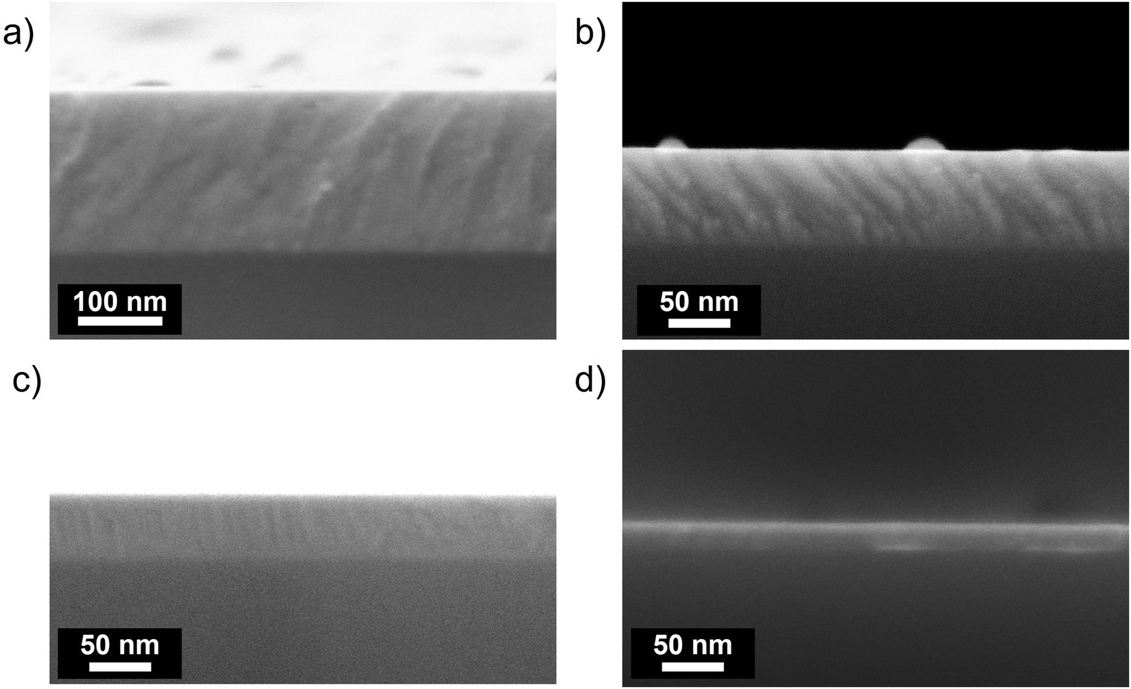 | ||
| Fig. 1 SEM cross-sectional micrographs of vacuum-annealed Ta(5%):TiO2 films deposited on a Si substrate with different thicknesses (a) 200, (b) 100, (c) 50 and (d) 20 nm. | ||
Optical microscopy allowed for the surface investigation of films with thickness in the range of 50–200 nm, while thinner films did not provide any sizeable optical contrast. The average lateral size of the polycrystalline domains was measured to be 15–20 μm for Ta(5%):TiO2 and 25–30 μm for Ta(10%):TiO2 films. This difference can be ascribed to the different laser fluence employed during film depositions. The surface images of Ta(5%):TiO2 and Ta(10%):TiO2 200 nm-thick films captured by using polarized-light microscopy are shown in Fig. S2 (ESI†).
The average roughness of 200 nm-thick films of Ta:TiO2 and TiO2 (both vacuum- and air-annealed) was estimated by means of spectroscopic ellipsometry by employing the model described in the Experimental section, resulting in the range of 3 to 5 nm for all samples. These values are in agreement with the root mean square roughness measured by atomic force microscopy on selected samples (not shown).
The structural characterization of the films was performed via XRD. Fig. 2 shows the resulting diffractograms as a function of Ta content for vacuum-annealed films with a nominal thickness of 200 nm, compared to vacuum- and air-annealed TiO2 films. An initial investigation of the XRD patterns highlights that all the analysed films reveal only the presence of a crystalline anatase phase, while no rutile phase is observed. In addition, in both the tantalum-doped films neither the presence of tantalum oxide (Ta2O5) phases nor metallic tantalum aggregates are detected, suggesting the formation of homogeneous solid solutions.26
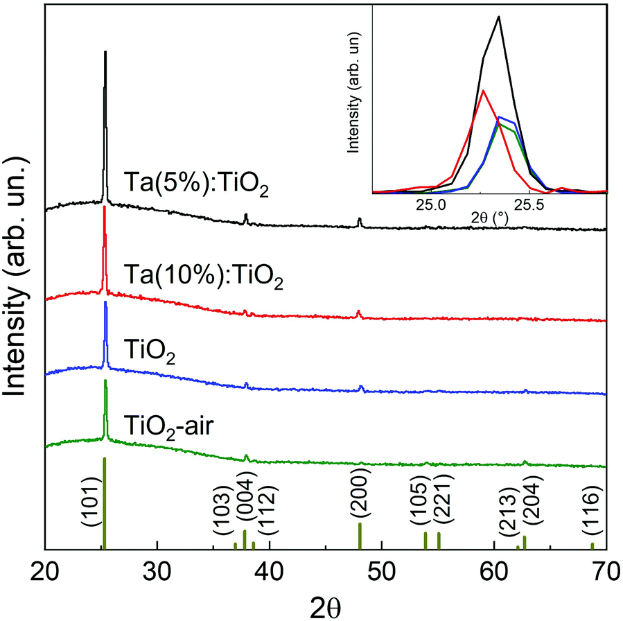 | ||
| Fig. 2 XRD diffractograms of air- and vacuum-annealed TiO2, Ta(5%):TiO2 and Ta(10%):TiO2 films with a nominal thickness of 200 nm. The inset shows the magnification of the (101) peak. The characteristic peaks of the anatase phase are highlighted at the bottom. | ||
In all the analysed films the more intense diffraction peak is the one associated with the (101) surfaces. This behaviour can be explained since it is known that anatase thin films grown on amorphous substrates preferably form [101]-oriented polycrystalline systems, since these possess the lowest surface energy.27,28 Interestingly, in both the Ta-doped films, the relative intensity of the (101) peak is higher than those in the TiO2 samples, suggesting that in the Ta-doped systems the doping could induce a preferential direction towards the lowest surface energy, namely the [101].
The atomic radius of Ta is slightly larger than the atomic radius of Ti, 145 and 140 pm, respectively, and, although the percentage of Ta is relatively low, this could introduce lattice distortions in the samples, which lead to a shift of the measured XRD peaks, as shown for the (101) peak in the inset of Fig. 2. A whole profile fitting performed on the films allows one to calculate the lattice parameters of the tetragonal cell of the TiO2 anatase phase, demonstrating a variation of the length for the a and c axes in relation to the Ta content. Specifically, in the Ta-doped films both the a and c axes are longer than in the pristine TiO2 films and their length increases with the Ta content (see Table 1).
| Sample | a [Å] | c [Å] | Volume [Å3] | τ [nm] |
|---|---|---|---|---|
| TiO2–air | 3.634 | 9.590 | 126.680 | 53 |
| TiO2 | 3.783 | 9.483 | 135.735 | 56 |
| Ta(5%):TiO2 | 3.793 | 9.498 | 136.646 | 76 |
| Ta(10%):TiO2 | 3.793 | 9.542 | 137.299 | 68 |
The process of doping also affects the crystallite size along the direction normal to the film surface, which can be calculated by using the Pawley method on diffractograms as described in the Experimental section, and in fact both the Ta-doped films show a slightly larger mean domain size than the undoped TiO2 films. In particular, Ta(5%):TiO2 films display a larger domain size equal to 76 nm, while in Ta(10%):TiO2 this is reduced to 68 nm. Interestingly, the different annealing procedures, namely in a vacuum or air, on undoped TiO2 films do not produce a marked influence on the mean crystallite domain size that remains almost unchanged (i.e. 53 nm and 56 nm for air- and vacuum-annealed TiO2, respectively, see Table 1), while the lattice parameters and the cell volume show more notable differences, as already observed in the literature.15
Raman spectroscopy has been carried out for all Ta:TiO2 films down to 10 nm thickness. Fig. 3a shows the Raman spectra of vacuum-annealed Ta(5%):TiO2 thin films; all spectra display the Raman peaks of the anatase phase, while no presence of Ta2O5 or other TiO2 polymorphs is detected, confirming the XRD results. In particular, the superimposing of Eg(1), B1g(1), and B1g(2) peaks on the A1g and Eg(3) peaks of the anatase phase is evident around their nominal values, i.e. 144, 399, 519, 513, and 638 cm−1 for the thickest films (i.e. 75–200 nm).29,30 On the other hand, for thicknesses in the 10–50 nm range, only the Eg(1) and Eg(3) peaks are evident, probably because of the poor signal-to-noise ratio.31 The Raman spectra of Ta(10%):TiO2 films show the same trend as that described for the 5% Ta content (see Fig. S3, ESI†).
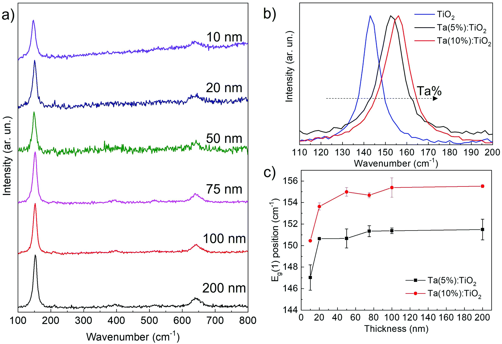 | ||
| Fig. 3 (a) Raman spectra of Ta(5%):TiO2 films with different thicknesses, i.e. from 10 up to 200 nm; (b) magnification of the Eg(1) peak of Raman spectra of films with different Ta content (5, 10 at% and bare TiO2) with a thickness of 200 nm; (c) centre energy of the fitted Eg(1) peak as a function of the film thickness for different Ta contents. | ||
The Ta content also affects the position of the Eg(1) peak, as demonstrated in Fig. 3b; for 200 nm films, the Eg(1) peak shifts from 144 cm−1 to 152 and to 155 cm−1 for Ta(5%):TiO2 and Ta(10%):TiO2, respectively, while the peak FWHM broadens from about 10 to 13–14 cm−1. This trend has been already observed in the literature and is associated with the correlation between the Eg(1) peak position and the measured charge carrier density, independently of the type and amount of extrinsic doping, or the specific deposition and annealing conditions.32Fig. 3c highlights the evolution of the Eg(1) peak position as a function of film thickness. At a fixed Ta content, the Eg(1) energy does not significantly depend on the thickness, at least down to 20 nm (in agreement with the measured charge carrier density, see the next section). On the other hand, for 10 nm-thick films the Eg(1) energy shifts for both Ta contents, namely to 147 and 150 cm−1, respectively, while the peak FWHM increases up to 17–18 cm−1. This behaviour can be associated with a larger film defectivity, size confinement as well as a smaller charge carrier density.29
Electrical properties
Fig. 4 reports the resistivity (ρ), charge carrier density (Ne), and Hall mobility (μ) measured for Ta:TiO2 specimens as a function of thickness (from 10 to 200 nm) and Ta content. Measurements on bare TiO2 films (thicknesses of 50, 100 and 200 nm), synthetized and annealed in a vacuum under the same conditions as that of the Ta:TiO2 films, are reported as reference (blue triangles). Notably, stoichiometric TiO2 is expected to be insulating, as confirmed from the measurements on PLD TiO2 films annealed in air (for which the resistivity was too high for the accessible range of our experimental setup). In this case, TiO2 films obtained by PLD at 1 Pa O2 after vacuum annealing treatment display a resistivity of about 10−2 Ω cm and a charge carrier density of 5–7 × 1019 cm−3, in agreement with the work of Mazzolini et al.15 This behaviour can be associated with a TiO2 anatase phase with oxygen vacancies induced by the atmospheric conditions during deposition and annealing, which represent an effective doubly negative charged donor state.15,33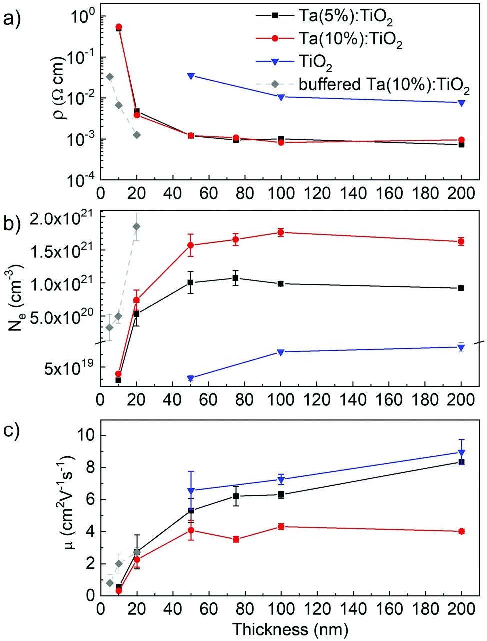 | ||
| Fig. 4 (a) Resistivity (ρ), (b) charge carrier density (Ne) and (c) Hall mobility (μ) as a function of film thickness (from 10 to 200 nm) and Ta content: Ta(5%):TiO2 (black squares), Ta(10%):TiO2 (red circles), bare TiO2 (blue triangles) and Ta(10%):TiO2 ultra-thin films deposited on a buffer layer of insulating 50 nm-thick TiO2 (grey rhombus). | ||
For Ta:TiO2 films, the resistivity is up to one order of magnitude lower than that of bare TiO2 for both Ta contents, i.e. down to 10−3 Ω cm, because of conduction electrons from the Ta active dopants (see Fig. 4a). Focusing on Ta(5%):TiO2 films, the resistivity is almost constant for thicknesses ranging from 200 down to 50 nm, with a slight increase from 8 × 10⁻⁴ up to 1 × 10⁻³ Ω cm, while a more evident increment occurs for 20 nm-thick films, where the resistivity reaches 3 × 10⁻³ Ω cm. The same trend is found for Ta(10%):TiO2, where resistivity is around 1 × 10⁻³ Ω cm for films in the 50–200 nm thickness range, while it increases to about 2 × 10⁻³ Ω cm for 20 nm-thick films.
As for resistivity, the charge carrier density does not significantly vary with thickness down to 50 nm for both doping contents (Fig. 4b). The values of ρ and n of Ta(5%):TiO2 films are in agreement with the previous work of Mazzolini et al., where polycrystalline Ta:TiO2 150 nm-thick films with the same Ta content were synthetized under the optimal oxygen sub-stoichiometric conditions.15 However, the resistivity of this work is slightly higher (the lowest one is around 8 × 10⁻⁴ Ω cm instead of 5 × 10⁻⁴ Ω cm) likely due to a slight decrease of the Hall mobility (see below). In addition, the same order of magnitude of resistivity was found for polycrystalline Nb:TiO2 thin films with thickness above 100 nm.8,34–36
On the other hand, the stability of the electrical properties down to a thickness of 50 nm is a novel and interesting result. Indeed, in a previous work, Liu et al. synthetized thin films of Nb and Ta co-doped TiO2 (nominal content of 3 at% for both Nb and Ta) and the effect of the thickness was studied in the range of 50–500 nm.31 They found an increase of the resistivity by more than one order of magnitude when reducing the film thickness from 500 to 200 nm (i.e. from about 9 × 10⁻⁴ to 1 × 10⁻² Ω cm), and even worse with a further reduction in thickness. In addition, even if the doping content was kept constant, the charge carrier density varied with the thickness, i.e. 2.3 × 10²⁰, 3.1 × 10²⁰ and 1.1 × 1021 cm−3 for thicknesses 50, 200 and 500 nm, respectively, and this behavior was associated with crystalline defects.
In our films, the carrier density Ne varies with the Ta content in the 50–200 nm thickness range. Indeed, the Ne of the Ta(10%):TiO2 films is almost twice that of Ta(5%):TiO2, with average values in the 50–200 nm thickness range of about 1.65 × 10²¹ and 9.95 × 1020 cm−3, respectively. For 20 nm-thick films, the charge carrier density is slightly smaller than in thicker films for both Ta contents, but Ta(10%):TiO2 films still show a higher value than Ta(5%):TiO2 (7.4 × 1020 cm−3 against 5.3 × 1020 cm−3, respectively). These results indicate that the charge carrier density increases proportionally with the Ta content under the condition of high dopant activation efficiency (calculated values of 74% and 68% for Ta(5%):TiO2 and Ta(10%):TiO2, respectively, with respect to the measured EDS concentrations) as observed for thicker films as well.18,32 In addition, the measured charge carrier density is in good agreement with the observed energy shift of the Eg(1) Raman peak, which increases with the Ta content and decreases for films thinner than 20 nm.
For 200 nm-thick films, the Ta content significantly affects the Hall mobility (Fig. 4c). Indeed, while the mobility μ measured for Ta(5%):TiO2 is almost the same as that for bare TiO2 (i.e. around 8 cm2 V−1 s−1), the Hall mobility of Ta(10%):TiO2 is reduced by a factor of about 2. This behaviour is mostly related to the higher concentration of ionized impurities in the crystal lattice, which affects electron scattering as well as the higher probability of carrier–carrier and carrier–defect interaction at larger values of Ne.8,32 Moreover, the Hall mobility for Ta(5%):TiO2 decreases gradually from about 8 down to about 5 cm2 V−1 s−1 for thicknesses varying from 200 down to 50 nm, while it reaches a value of about 1.5 cm2 V−1s−1 for 20 nm-thick films. On the other hand, the mobility remains almost constant and around 4 cm2 V−1 s−1 for Ta(10%):TiO2 films down to 50 nm and decreases to about 2 cm2 V−1 s−1 for 20 nm-thick films. This trend can be related to the reduction of the characteristic grain size as well as to the presence of defects such as grain boundaries or dislocations affecting the mobility.37 Indeed, the mean crystalline domain size calculated from XRD measurements (76 nm and 68 nm for Ta(5%):TiO2 and Ta(10%):TiO2, respectively) confirms that the higher Hall mobility of Ta(5%):TiO2 is also accompanied by larger grains; moreover, a significant decrease of μ for decreasing thicknesses is expected for thicknesses much smaller than the calculated mean domain size, such as in 20 nm-thick films, where crystalline grains cannot develop completely.
On the other hand, 10 nm-thick films display a radically different electrical behaviour, almost independent of the Ta content. Indeed, for both Ta(5%):TiO2 and Ta(10%):TiO2 10 nm-thick films, the resistivity measured is about 0.5 Ω cm, i.e. more than two orders of magnitude higher than in thicker Ta:TiO2 films (see Fig. 4a). Hall effect measurements on these films were less reliable and reproducible, probably because of the higher resistance of the film as well as the difficulty to measure such a thin film with our setup. The measured charge carrier density was 2.3 and 3.5 × 1019 cm−3 for 5 and 10 at% Ta contents, respectively, namely around 2 orders of magnitude smaller than in thicker films (Fig. 4b). At the same time, the Hall mobility decreases by one order of magnitude with μ = 0.56 cm2 V−1 s−1 for Ta(5%):TiO2 and μ = 0.31 cm2 V−1 s−1 for Ta(10%):TiO2 films (Fig. 4c). This behavior can be explained with the presence of defects at the film surface and at the interface with the substrate, causing electron trapping and scattering that become dominant in ultra-thin films with a thickness below 20 nm, as already observed in previous studies on ultra-thin films of AZO,37–39 together with the smaller domain size as discussed before.
The electrical properties of ultra-thin Ta:TiO2 films can be enhanced by exploiting an appropriate buffer layer that improves the wettability and the interface quality and reduces the high defectivity promoted by growing the films on lattice-mismatched substrates (e.g. glass and silicon).39–43 In this case, we investigated the effect of a 50 nm-buffer layer of polycrystalline stoichiometric TiO2 (air-annealed) in the anatase phase on the growth of Ta(10%):TiO2 films with 5, 10 and 20 nm thicknesses. The TiO2 buffer layer alone is insulating and the measured electrical properties of the buffered films are reported in Fig. 5 (grey diamonds), showing an improvement for both 10 and 20 nm thick films. In particular, the buffered 20 nm-thick film displays a decrease in resistivity and an increase in charge carrier density up to values similar to the unbuffered Ta(10%):TiO2 films with 50–200 nm thickness, while the buffered 10 nm-thick films show improvement in all the measured electrical properties to values similar to those of the unbuffered 20 nm-thick films. Finally, since the buffer layer favours a better wettability of the growing film onto the substrate, we were able to deposit conductive Ta(10%):TiO2 films with a thickness as low as 5 nm, which is unaffordable by depositing directly on glass, even though the electrical properties show a deterioration. These results highlight the possibility of designing devices with ultra-thin conductive films, replacing metals which present a percolation threshold.22
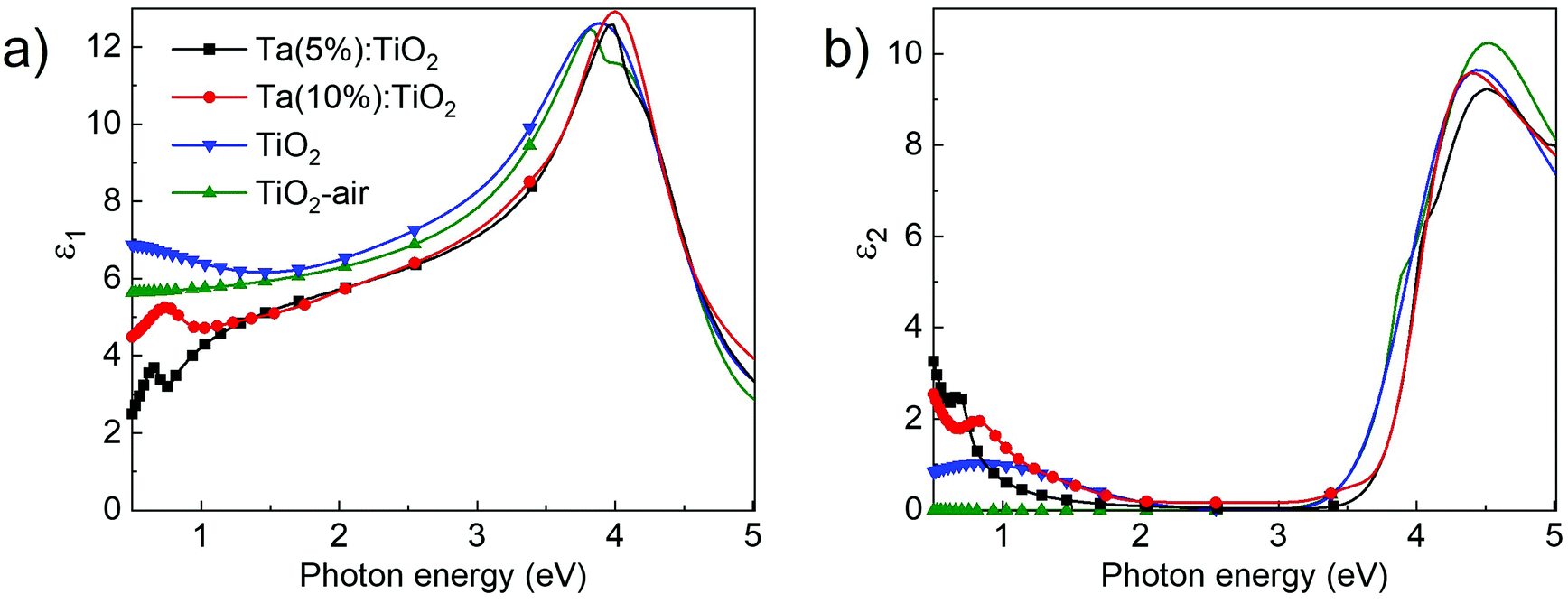 | ||
| Fig. 5 (a) Real and (b) imaginary parts of the dielectric constant of Ta:TiO2 films with different doping levels (5 and 10 at%) compared with those of bare vacuum-annealed (TiO2) and air-annealed (TiO2–air). | ||
Optical properties
Ellipsometric measurements were performed on Ta:TiO2 films with 200 nm nominal thickness, grown on Si substrates covered by a few-nm thick native SiO2 layer as described in the Experimental section. The corresponding ψ and Δ measurements are shown in Fig. S5 of the ESI.†Fig. 5a and b report the real (ε1) and the imaginary (ε2) part of the dielectric functions extracted by means of the optical model described in the Experimental section. The results of Ta:TiO2 films with Ta contents 5 and 10 at% are compared to those of bare TiO2 with the same nominal thickness, both air-annealed and vacuum-annealed. The corresponding refractive index and extinction coefficient are reported in Fig. S5 (ESI†).For the real part (ε1, Fig. 5a), air-annealed TiO2 shows two humps in the high-energy region (3.5–4.5 eV), while vacuum-annealed TiO2 shows a unique band in the same range. In the visible range, ε1 decreases with decreasing energy for both air- and vacuum-annealed TiO2 with almost the same slope. For both samples, ε1 values are in accordance with those reported in the literature for the anatase phase over the investigated spectral range, with a maximum around 12.5 at 3.8–3.9 eV and a value between 6 and 9 in the visible range (1.7–3.3 eV).44–47 In the near-IR range, ε1 is flat for air-annealed TiO2, while its value increases for decreasing energy for vacuum-annealed TiO2. On the other hand, Ta doping leads to blue-shifted and narrowed features in the UV range, while the maximum values of ε1 are close to those of bare TiO2. In the visible range, the ε1 curves of Ta:TiO2 films almost overlap and decrease as in bare TiO2 films but at lower values (this behaviour has been already reported by Manole et al. for the Nb-doped anatase phase),48 while in the near-IR range ε1 decreases, as expected by the free-carrier contribution that sets the plasma frequency in the mid-IR spectral range.
In Fig. 5b, ε2 of air-annealed TiO2 exhibits a band in the UV range associated with optical band gap absorption with a peak around 4.5 eV and a shoulder around 3.8 eV. This shape is associated with the anisotropy of the crystal structure in the anatase phase, which results in the optical properties being strongly dependent on the polarization direction of the incident light beam. Indeed, the shoulder and the peak are associated with the perpendicular and parallel components (with respect to the c-axis) of the dielectric tensor.44,45,49 Similar to ε1, also ε2 shows a single feature in the UV range for vacuum-annealed TiO2 at the same energy as that of air-annealed TiO2, but with a slightly smaller value. The effect of Ta doping is the shift of the absorption band in the UV range towards higher energy values, suggesting a larger optical band gap with respect to bare TiO2 films, due to the Moss–Burstein effect (see next section).50,51 In the visible range, all ε2 curves are close to zero, suggesting no absorption as expected for TiO2 and TiO2-based TCOs. In the lower-energy region of the visible range (below 2 eV) and in the near-IR range, ε2 of air-annealed TiO2 curve is close to zero, while for vacuum-annealed TiO2 it increases to a maximum around 0.84 eV. The different behaviour of vacuum-annealed TiO2 with respect to air-annealed TiO2 in this range can be associated with the oxygen vacancy concentration in the anatase structure (as already discussed in the previous section).52,53 On the other hand, Ta:TiO2 films show a larger increase of ε2 in this range, which is again consistent with a prominent plasma response in the mid-IR region.
The behavior of the real and imaginary parts of the dielectric constant of both Ta:TiO2 films is in accordance with previous studies where the refractive index and the extinction coefficient in the UV and visible ranges of Ta:TiO2, Nb:TiO2 and Ta and Nb co-doped thin films are reported.19,48,54,55 The optical properties in the near-IR range show an absorptive behavior associated with the tail of free carrier (plasma) oscillations that play a role below the screened plasma frequency range. This trend was observed in the work of Neubert et al., who performed ellipsometry on polycrystalline anatase Ta:TiO2 films synthetized by means of DC magnetron sputtering (Ta = 2 at%, thickness 300–400 nm),19 and in the theoretical work of Muhammady et al., regarding the calculation of the dielectric function of Ta:TiO2 (Ta = 6.25 at%) in anatase phase by employing the Drude–Lorentz model.56 In both cases this behavior was associated with the free carrier contribution, as already observed for other TCOs in thin film forms (e.g. ITO, AZO and Ga-doped ZnO), for which the occurrence of plasmonic excitations has been verified.57,58 Finally, the onset of the metallic behavior is expected to blue-shift with charge carrier density,59 as observed on comparing Ta(5%) and Ta(10%):TiO2.
Notably, both Ta:TiO2 films show a peak in the near-IR range in ε2 curves at 0.68 and 0.82 eV for Ta contents of 5 and 10 at%, respectively, that correspond to dispersive features in the ε1 curve in the same range. The explanation of the weak features in the near-IR range is not straightforward. A tentative hypothesis is the establishment of a strong interaction between plasma oscillation of free carriers and phonons, with a formation of longitudinal optical phonon–plasmon coupled modes. This phenomenon is typical for polar semiconductors and it occurs in the IR dielectric response,60,61 which can be described by a harmonic oscillator function with a Lorentzian line shape.62 Although Ta:TiO2 is not a polar material, the large carrier density due to Ta doping as well as the large degree of lattice defects could induce an increase in the ionic character of the Ti–O covalent bond.
The optical constants extracted from ellipsometry were directly applied to the modelling of normal-incidence transmission spectra, by allowing only for small adjustments in the oscillator parameters to account for the different soda-lime substrate compared to the silicon one. In Fig. 6, experimental data from the transmission measurements are shown (squares) along with the fit data (continuous lines), which are the outcomes of the modelling. The respective dielectric constants, refractive index and extinction coefficients that came out of the modelling of this system are shown in Fig. S6 (ESI†). Indeed, transmittance spectra confirm the optical behaviour observed with the previous analysis of the dielectric function. For all the spectra, the transmittance goes to zero in the UV range due to interband absorption, while it increases in the visible and near-IR ranges. The oscillations in this range are due to thin-film interference and are related to the film optical path length.8,63 Vacuum-annealed TiO2 displays lower transmittance intensity than air-annealed TiO2 in the energy range from visible to near-IR associated with absorption by oxygen vacancies, while both Ta:TiO2 films show a stronger decrease in the transmittance in the near-IR range due to free carrier absorption related to the response of the conduction plasma. Furthermore, the effect of increasing the Ta content is observed as a blue-shift of the absorption edge in the UV range, because of the Moss–Burstein effect, as previously explained.
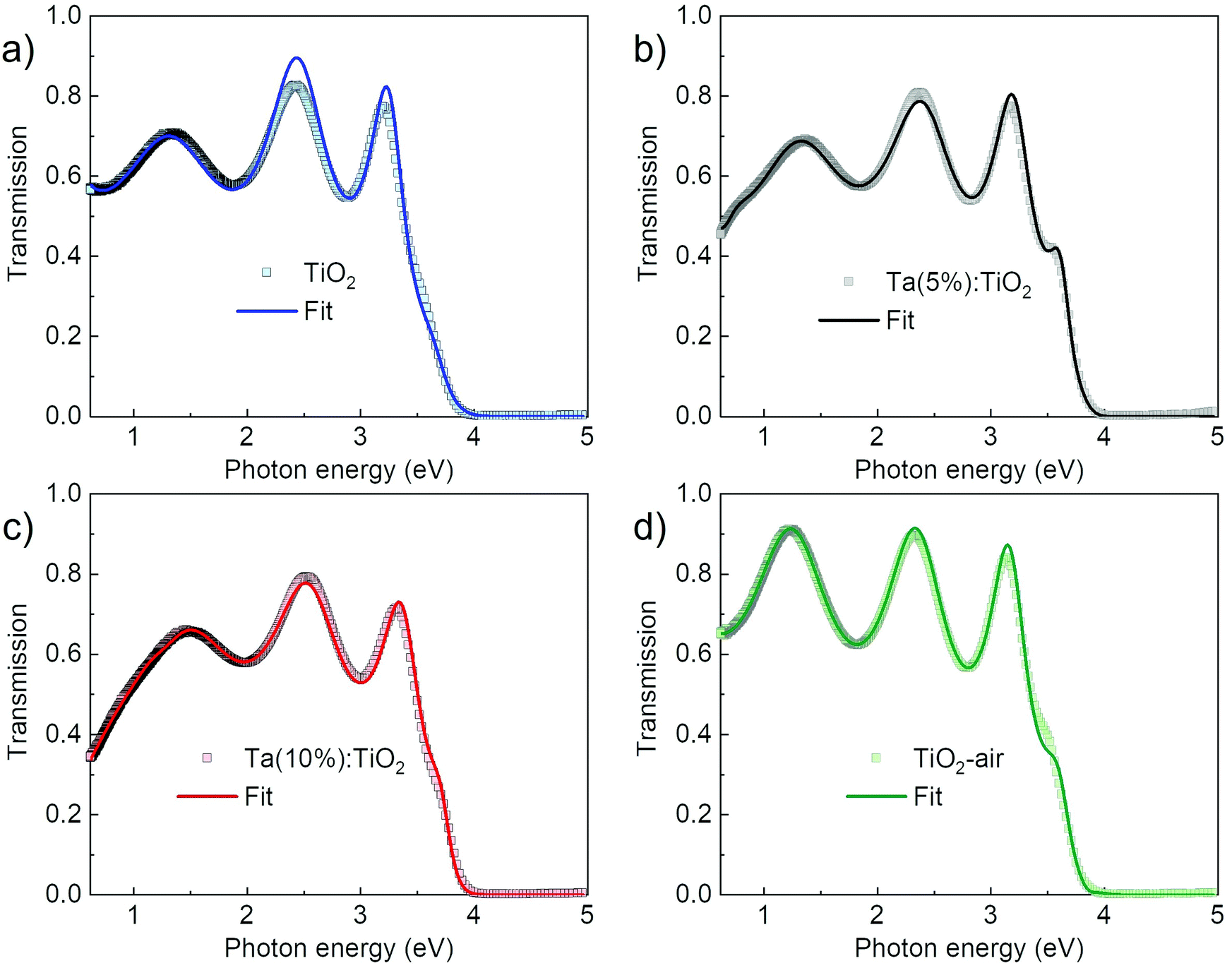 | ||
| Fig. 6 Transmission measurements of vacuum-annealed (a) TiO2, (b) Ta(5%):TiO2, (c) Ta(10%):TiO2 and (d) air-annealed TiO2 films of 200 nm thickness, grown on soda-lime glass substrates. Squares represent the experimental data while lines represent the theoretical fit, as extracted from ellipsometry measurements. | ||
Fig. 7a and c show the optical transmittance spectra as a function of film thickness, from 10 nm up to 200 nm, of Ta(5%):TiO2 and Ta(10%):TiO2 films. Thickness reduction leads to an increase in transmittance in the visible and near-IR ranges because of the reduced absorption, according to the Lambert–Beer law, while interference fringes change according to the optical path length.63 This modulation of fringe position is a feature that can be exploited in applications in which TCO films are employed as transparent electrodes and a fine tuning of the film transparency at specific wavelengths is required. The effect of thickness in the UV range is more appreciable looking at the absorption coefficient (α), reported in Fig. 7b and d as a function of energy, as evaluated from the Lambert–Beer law (see the Experimental section). The absorption coefficient shows the onset of the absorption band, which does not depend on the thickness down to 50 nm, while it redshifts for 10 and 20 nm-thick films.
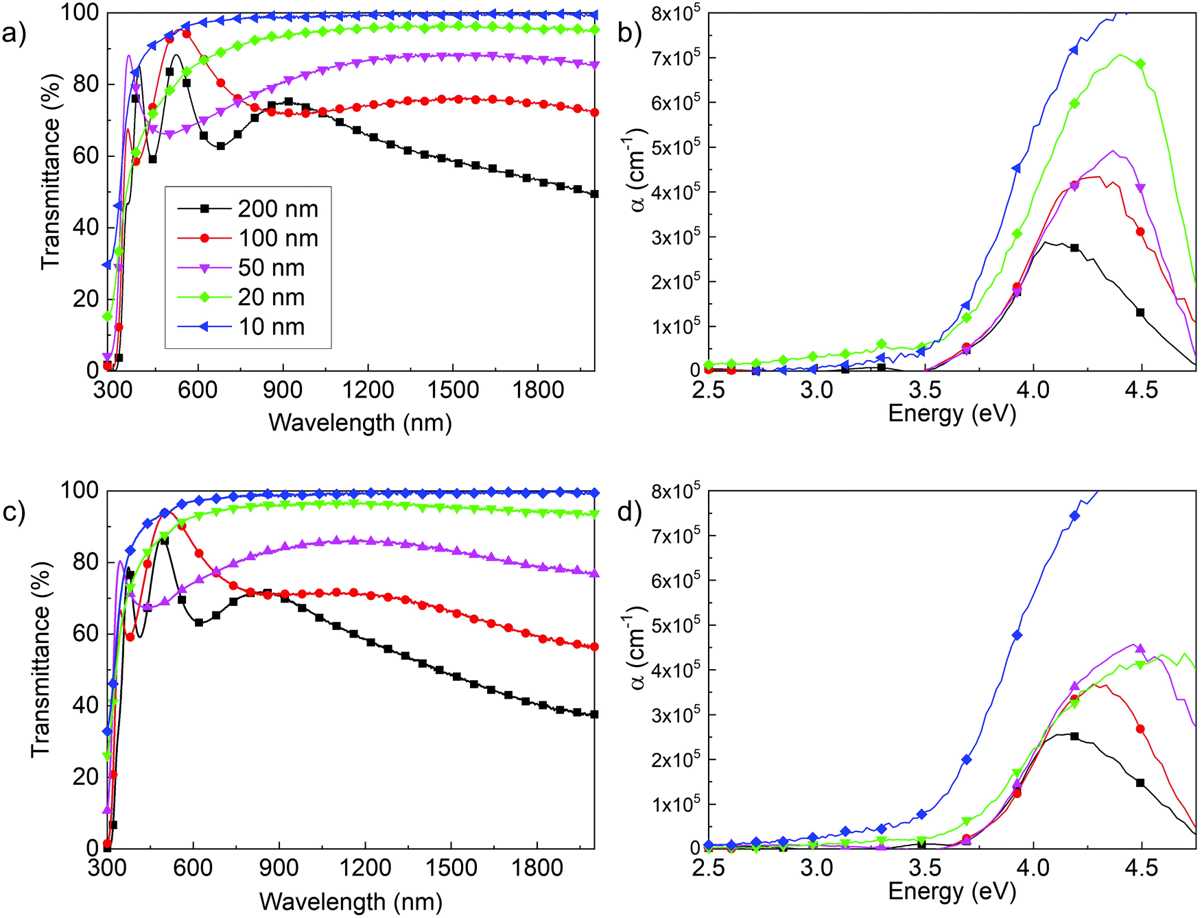 | ||
| Fig. 7 Optical transmittance and absorption coefficient (α) as a function of thickness (10–200 nm) of (a and b) Ta(5%):TiO2 and (c and d) Ta(10%):TiO2 films; the legend of all images is in figure (a). | ||
Discussion
The optical gap (Egap) of Ta:TiO2 thin films was calculated by means of a Tauc plot of the absorption coefficient (see the Experimental section) and the results are reported in Fig. 8 as a function of Ta content and thickness. As a reference, the results of 20, 50 and 200 nm-thick vacuum-annealed TiO2 films are also reported and the calculated band gap is about 3.29 eV, in line with the band gap of the anatase phase, namely 3.2–3.4 eV.10,46 A very similar value of Egap was obtained for air-annealed TiO2 films.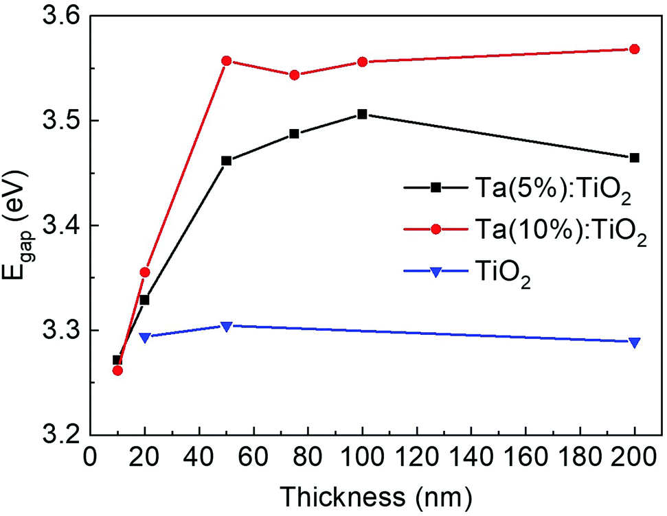 | ||
| Fig. 8 Optical band gap as a function of thickness (10–200 nm) and Ta content (bare TiO2, 5 and 10 at%) calculated via the Tauc plot. | ||
For the thickest Ta:TiO2 films, i.e. in the 50–200 nm range, Egap increases with the Ta content as a consequence of the Moss–Burstein effect, where free carriers partially fill the conduction band forcing higher energy optical transitions.50 Indeed, the measured charge carrier density of Ta(10%):TiO2 is almost twice that of Ta(5%):TiO2. Congruently, the average band gap calculated for 50–200 nm TiO2 films doped with 5 and 10 at% of Ta was 3.48 and 3.56 eV, respectively. The value of Egap of Ta(5%):TiO2 films agrees with the work of Mazzolini et al., in which a gap of 3.46 eV was found for the optimal synthesis conditions.15 In addition, the blue-shift of the Egap in this energy range with doping content has been already observed in other studies on Ta:TiO2 and Nb:TiO2 thin films when considering a similar amount of dopant atoms.36,54,64,65 Specifically, the Moss–Burstein effect responsible for the Egap blue-shift occurs because of the increase of charge carrier density, and it is typical for TCOs. Indeed, in the work of Bin-Bin et al., Ta:TiO2 thin films were deposited by PLD with a fixed Ta content (4 at%) and the Egap was found to vary with the post-deposition thermal treatment because of the different amounts of measured charge carrier density.66 Even in this case, for the same measured value of carrier density, the Egap agrees with the ones of this work. Finally, Liu et al. found an increase of Egap from 3.53 to 3.78 eV with the thickness from 50 to 500 nm for their Ta and Nb co-doped TiO2 films (already described in the Electrical properties section) because of the increase of charge carrier density,31 while in our study the charge carrier density and, as a consequence, the Egap of the films of thickness 50–200 nm is almost constant. On the other hand, Egap calculated for 10–20 nm-thick films decreases down to the value expected for an undoped film, in agreement with the trend of the charge carrier density which starts to decrease for 20 nm films, down to a value typical of undoped TiO2 for 10 nm-thick films.
To support this analysis, the optical band gap was calculated from ellipsometric measurements as well. The Tauc plot with α extracted from ellipsometry for 200 nm-thick films gives results in agreement with the previous findings, i.e. 3.28 eV for bare TiO2, as well as 3.46 and 3.53 eV for Ta(5%):TiO2 and Ta(10%):TiO2, respectively.
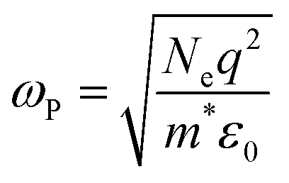
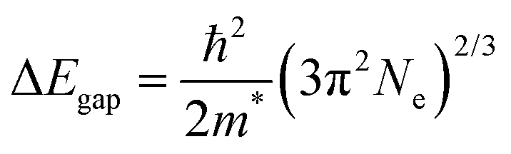
Another important property for a TCO is the effective mass (m*) of electrons in the conduction band. For the calculation of m* we used the Drude model, which describes the motion of free electrons moving against a fixed background of positive ions, while the overall lattice potential effect is taken into account by m*:
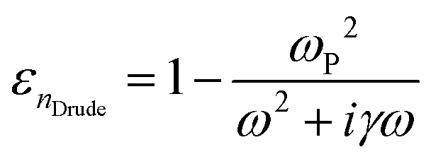 | (1) |
 | (2) |
 and a parallel one
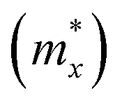
 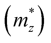 with respect to the tetragonal axis, which are equal to 0.4–0.6 me and >3.5 me, respectively. Moreover, the calculations predict an increase of
  with the charge carrier concentration.16 Taking into account that the Ta:TiO2 films reported in this study are polycrystalline, our m* results are consistent with the reported calculated
  and
and  values and, at the same time, m* shows an increase with the Ta content.
An independent estimate of m* can also be obtained from the optical bandgap increase as a function of the charge carrier density due to the Moss–Burstein effect. In a simplified parabolic-band picture, the shift in the optical band gap follows the equation:69
 | (3) |
Finally, we provide an estimate for the screened plasma energy (EP) by revisiting the ellipsometric fitting in the IR range and introducing a real-valued offset, indicated as ε∞, to take the contribution of the bound electrons of the semiconductor into account. The value of ε∞ (equal to about 5.9 and 6.0 for Ta(5%):TiO2 and Ta(10%):TiO2, respectively, in good agreement with the literature),73,74 allows calculating the screened plasma energy as 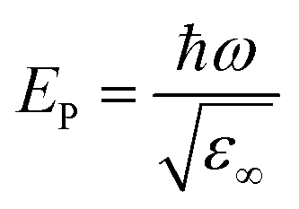 . The estimated EP value is about 0.2 eV for both Ta(5%):TiO2 and Ta(10%):TiO2. It should be noted that this estimate is obtained by extrapolating the ellipsometry model out of the measured range and, thus, must be considered only as a rough indication of the expected plasma energy values. However, these findings can be crosschecked against reflectance and trasmittance spectra collected in the 0.1–1.49 eV range by means of Fourier Transform infrared spectroscopy (FTIR, see Fig. S7 of the ESI†). For both doping levels, a reflectivity increase, which is a typical signature of the onset of the plasmonic behavior, is observed in the 0.2–0.3 eV range, in good agreement with the ellipsometric extrapolation. No reflectance decrease is instead observed for bare TiO2 films. These EP values in the near- and mid-IR ranges are expected for a TCO with the charge carrier density of the order of 1021 cm−3.59,75 Unfortunately, no straightforward and physically meaningful combination of Drude and Lorentz contributions allows fitting the FTIR data, a fact that reveals a possibly higher level of complexity and will be the subject of future studies.
Conclusions
In this work, Ta-doped TiO2 thin films were investigated as a function of Ta content (5 and 10 at%) and thickness (in the 10–200 nm range), focusing on their structural, electrical, and optical properties, while comparing the results with those of bare TiO2. Homogeneous and compact Ta:TiO2 films were synthetized via pulsed laser deposition followed by a vacuum thermal treatment, obtaining poly-crystalline films in the anatase phase with preferential growth along the (101) direction.The effect of the Ta content on the electrical properties is found to depend on the thickness. For films in the 50–200 nm range, the measured resistivity is between 8 × 10⁻⁴ and 1 × 10⁻³ Ω cm for both Ta contents, while the charge carrier density Ne increases proportionally to the Ta content, suggesting a condition of high dopant activation efficiency. On the other hand, the Hall mobility decreases with the Ta content due to a higher concentration of ionized impurities in the crystal lattice, which affects the electron scattering at higher values of Ne. The electrical properties deteriorate for films thinner than 20 nm almost independently of the Ta content, but still conductive films are obtained with 10 nm thickness (with a resistivity of about 0.5 Ω cm). In addition, the electrical properties of ultra-thin films demonstrated an enhancement by employing a 50 nm-thick buffer layer of polycrystalline and stoichiometric TiO2. In this case, conductive films were obtained down to a thickness of 5 nm. This result highlights the possibility of designing devices with ultra-thin conductive films, which is a thickness difficult to achieve with metals.
Optical characterization shows that the Ta doping changes the optical response as a consequence of the increased charge carrier density. Indeed, the optical absorption in the UV range blue-shifts with the Ta content, according to the Moss–Burstein effect, while the absorption in the IR range increases because of free carriers.
The estimated optical band gaps increase with the Ta content for films of 50–200 nm thickness, while it starts to decrease for films of 20 nm thickness, down to a value typical for undoped TiO2 films with 10 nm thickness.
Notably, both the electrical and the optical properties demonstrated no relevant changes in the thickness range from 200 nm down to 50 nm.
The effective mass of Ta:TiO2 films was estimated as well, and the results are in accordance with theoretical calculations from the literature for a Ta-doped anatase phase. Moreover, the predicted increment of the effective mass with the Ta content is confirmed. Finally, the plasma energy was calculated to be in the near/mid-IR range, as expected for a TCO with a charge carrier density of the order of 1021 cm−3.
The overall results, especially the fine tunability of the electrical and optical properties by means of the Ta content and the investigation of the thickness dependence of the film properties, show that Ta:TiO2 films could be suitable as transparent conductive components in optoelectronic applications as well as for plasmonic applications in the IR range.
Experimental section
PLD was performed in a vacuum chamber equipped with mass flow controllers to tune the partial gas pressure. Ablation was performed with a ns-pulsed laser (Nd:YAG, 2nd harmonic, λ = 532 nm) with pulse duration in the 5–7 ns range and a repetition rate of 10 Hz. The laser pulses were focused on the target material through a viewport and the target was mounted on a roto-translational manipulator ensuring a uniform ablation. Ta:TiO2 thin films with a nominal content of Ta = 5, 10 at% were grown by ablating 2 inch targets of Ta2O5:TiO2 with a molar ratio equal to 0.025![[thin space (1/6-em)]](https://www.rsc.org/images/entities/char_2009.gif) :0.975 and 0.05:0.95, respectively (99.99% pure, provider “Testbourne Ltd”), while pure TiO2 films were obtained from a 99.9% pure TiO2 target (provider “Kurt J. Lesker”). We name the doped films Ta(5%):TiO2 and Ta(10%):TiO2, according to their nominal content of Ta. The laser fluence (F) on the target was set at 2.27 J cm−2 for the deposition of TiO2 and Ta(5%):TiO2, while F = 2.73 J cm−2 was employed for Ta(10%):TiO2. Depositions were performed at room temperature and in a pure O2 background at a pressure of 1 Pa. The employed substrates were Si(100) and soda-lime glass cleaned in an ultrasonic bath with isopropanol and mounted on a rotating sample holder at a fixed target-to-substrate distance of 50 mm. Thin films with different nominal thicknesses, from 10 to 200 nm, were deposited by varying the deposition duration and the actual thickness values were evaluated by means of a field emission scanning electron microscope (FEG-SEM, Zeiss SUPRA 40) on samples grown on silicon. The deposition rate is related to the laser fluence and was estimated around 11 nm min−1 for TiO2 and Ta(5%):TiO2 and 18 nm min−1 for Ta(10%):TiO2. The FEG-SEM microscope is equipped with an Oxford Instruments Si(Li) detector for energy-dispersive X-ray spectroscopy (EDS), which was employed in this work to estimate the tantalum atomic percentage (at%) with an accelerating voltage of 10 kV.
:0.975 and 0.05:0.95, respectively (99.99% pure, provider “Testbourne Ltd”), while pure TiO2 films were obtained from a 99.9% pure TiO2 target (provider “Kurt J. Lesker”). We name the doped films Ta(5%):TiO2 and Ta(10%):TiO2, according to their nominal content of Ta. The laser fluence (F) on the target was set at 2.27 J cm−2 for the deposition of TiO2 and Ta(5%):TiO2, while F = 2.73 J cm−2 was employed for Ta(10%):TiO2. Depositions were performed at room temperature and in a pure O2 background at a pressure of 1 Pa. The employed substrates were Si(100) and soda-lime glass cleaned in an ultrasonic bath with isopropanol and mounted on a rotating sample holder at a fixed target-to-substrate distance of 50 mm. Thin films with different nominal thicknesses, from 10 to 200 nm, were deposited by varying the deposition duration and the actual thickness values were evaluated by means of a field emission scanning electron microscope (FEG-SEM, Zeiss SUPRA 40) on samples grown on silicon. The deposition rate is related to the laser fluence and was estimated around 11 nm min−1 for TiO2 and Ta(5%):TiO2 and 18 nm min−1 for Ta(10%):TiO2. The FEG-SEM microscope is equipped with an Oxford Instruments Si(Li) detector for energy-dispersive X-ray spectroscopy (EDS), which was employed in this work to estimate the tantalum atomic percentage (at%) with an accelerating voltage of 10 kV.
All the as-deposited TiO2-based thin films were amorphous, therefore post deposition annealing treatments in a vacuum atmosphere (p < 4 × 10⁻⁵ Pa) in a homemade furnace at 550 °C (10 °C min−1 ramp, 1 h dwell) were employed to obtain polycrystalline anatase films, according to previous studies.76
The thin film surfaces were investigated by means of optical microscopy (Leitz orthoplan-pol). Structural characterization was carried out by X-ray diffraction (XRD) and Raman spectroscopy. XRD patterns were collected using a Bruker D8 Advance X-ray diffractometer at 293 K (Cu Kα1 radiation – 1.5406 Å). The measurements were carried out in a Bragg–Brentano geometry with a step-scan technique and a 2θ range of 10–70°. Data were acquired by using a Lynx Eye detector in continuous scanning mode with a step size of 0.038° and a time step of 0.15 s. The mean crystallite size domain (τ) along the film growth direction and the lattice parameters of the samples were determined by using the full profile fitting Pawley method.77 The Pawley method was carried out using the program-suite TOPAS from Bruker. Raman spectra of the samples were collected using a Renishaw InVia micro Raman spectrometer with an argon ion laser (514 nm), with a laser power of 0.13 mW and a spectral resolution of about 3 cm−1.
Electrical characterization and Hall effect measurements were performed on TiO2 and Ta:TiO2 films deposited on soda-lime glass in a four-point probe configuration with a Keithley K2400 source/measure unit as a current generator (from 100 nA to 10 mA), an Agilent 34970A voltage meter, and a 0.57 T Ecopia permanent magnet.
Optical transmittance (T) and reflectance (R) spectra in the spectral range of 250–2000 nm were evaluated on samples deposited on soda-lime glass with a UV-vis-NIR PerkinElmer Lambda 1050 spectrophotometer with a 150 mm diameter integrating sphere. All the acquired spectra were normalized with respect to the glass substrate contribution. The absorption coefficient (α) was evaluated from the Lambert–Beer law α = −1/d[T/(1 − R)], where d is the film thickness. The optical energy gap (Egap) was calculated by means of a Tauc plot, where (αhν)nversus hν was plotted in the proximity of the absorption onset of the films in the UV range and the exponent n was chosen equal to 0.5 because of the indirect band gap of anatase; Egap was extrapolated with the intercept in the energy axis using a linear fit.
Fourier transform infrared spectroscopy (FTIR) was performed both in transmission and reflection geometries with a commercial instrument (INVENIO-R by Bruker), employing a halogen lamp emitting in the near-IR range and a globar source emitting in the mid-IR spectral range, together with a mercury cadmium telluride (MCT) detector to acquire spectra in the 0.1–1.49 eV spectral range. The beam incidence on the sample is almost normal (about 10° incidence angle) and the diameter of the beam in the focus is about 1 mm. For these measurements, films with a thickness of 670 nm (in order to have enough transmittance contrast in the measured range) were deposited on CaF2 substrates.
Spectroscopic ellipsometry (SE) was performed by means of a J. A. Woollam V-VASE ellipsometer (0.5–5.05 eV energy range, incidence angle of 60°). The analysis involves evaluating the ellipsometric angles ψ(λ) and Δ(λ), defined as 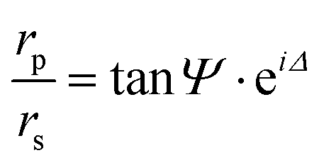 , where rp(s) is the Fresnel reflection coefficient for p(s)-polarized radiation. The measurement of amplitude and phase-related quantities adds a degree of precision, useful for deducing the dielectric function of materials, even with complex nanoscale morphology.78 From the optical point of view, the system was modelled as a stack of dielectric layers, with each of them being characterized by its thickness and complex dielectric function. The optical response of the system was calculated assuming Fresnel boundary conditions at the interface between the layers. Bottom to top, the model included: (i) a semi-infinite Si substrate, (ii) a native oxide layer, (iii) the Ta:TiO2 film and (iv) a roughness layer (the latter modelled as a Bruggemann effective-medium layer composed of 50% of Ta:TiO2 and 50% of voids). For the modelling of the optical properties of Ta:TiO2 films, we employed a combination of Lorentz, Lorentz–Gaussian and so-called PSEMI oscillators, along with a Drude-type contribution to take the doping-induced free carriers into account. PSEMI oscillators are parameterized functions widely employed to model the optical response of crystalline semiconductors.79,80 The oscillator parameters of the undoped TiO2, and the Ta:TiO2, layers, as well as the thickness of all the optical layers, were carefully fitted in order to achieve the best agreement between the experimental data and the simulated SE spectra. The thickness of the SiO2 native oxide was assessed by SE measurements on a bare substrate and was found to be around 2 nm.
Author contributions
Beatrice R. Bricchi: writing – original draft, writing – review & editing, data curation, formal analysis, investigation and conceptualization. Maria Sygletou and Giancarlo Terraneo: formal analysis, investigation and writing – review & editing. Luca Ornago: formal analysis, investigation, conceptualization and writing – review & editing. Cristina Mancarella, Lorenzo Stasi, Francesco Rusconi, Erika Mogni and Matteo Ghidelli: investigation and writing – review & editing. Andrea Li Bassi, Francesco Bisio and Paolo Biagioni: supervision, conceptualization writing – review & editing.Conflicts of interest
There are no conflicts to declare.Acknowledgements
The authors thank Prof. M. Canepa and Dr M. Magnozzi for useful discussion. This project has received funding from the European Union's Horizon 2020 research and innovation programme under the Marie Skłodowska-Curie grant agreement no. 799126.References
- S. C. Dixon, D. O. Scanlon, C. J. Carmalt and I. P. Parkin, J. Mater. Chem. C, 2016, 4, 6946–6961 RSC.
- D. H. Kim, S. Lee, J. H. Park, J. H. Noh, I. J. Park, W. M. Seong and K. S. Hong, Sol. Energy Mater. Sol. Cells, 2021, 96, 276–280 CrossRef.
- S. Dias, S. Chirakkara, N. Patel and S. B. Krupanidhi, J. Mater. Sci.: Mater. Electron., 2018, 29, 2131–2139 CrossRef CAS.
- T. Hanada, T. Negishi, I. Shiroishi and T. Shiro, Thin Solid Films, 2010, 518, 3089–3092 CrossRef CAS.
- S. H. Park, J. B. Park and P. K. Song, Curr. Appl. Phys., 2010, 10, S488–S490 CrossRef.
- D. S. Ginley and J. D. Perkins, Handbook of Transparent Conductors, Springer, Boston, MA, 2011 Search PubMed.
- F. Wang, M. Z. Wu, Y. Y. Wang, Y. M. Yu, X. M. Wu and L. J. Zhuge, Vacuum, 2013, 89, 127–131 CrossRef CAS.
- G. Wan, S. Wang, X. Zhang, M. Huang, Y. Zhang, W. Duan and L. Yi, Appl. Surf. Sci., 2015, 357, 622–625 CrossRef CAS.
- R. L. Moss, E. Tzimas, H. Kara, P. Willis and J. Kooroshy, Assessing Rare Metals as Supply-Chain Bottlenecks in Low-Carbon Energy Technologies, JRC Scientific and Technical Reports, EUR 24884, 2011.
- H. Tang, K. Prasad, R. Sanjinès, P. E. Schmid and F. Lévy, J. Appl. Phys., 1994, 75, 2042–2047 CrossRef CAS.
- A. Fujishima, T. N. Rao and D. A. Tryk, J. Photochem. Photobiol., C, 2000, 1, 1–21 CrossRef CAS.
- T. Bak, J. Nowotny, M. Rekas and C. C. Sorrell, Int. J. Hydrogen Energy, 2002, 27, 991–1022 CrossRef CAS.
- A. Hagfeldt, G. Boschloo, L. Sun, L. Kloo and H. Pettersson, Chem. Rev., 2010, 110, 6595–6663 CrossRef CAS PubMed.
- J. Osorio-Guillén, S. Lany and A. Zunger, Phys. Rev. Lett., 2008, 100, 036601 CrossRef PubMed.
- P. Mazzolini, P. Gondoni, V. Russo, D. Chrastina, C. S. Casari and A. Li, Bassi, J. Phys. Chem. C, 2015, 119, 6988–6997 CrossRef CAS.
- H. Anh Huy, B. Aradi, T. Frauenheim and P. Deák, J. Appl. Phys., 2012, 112, 016103 CrossRef.
- Y. Furubayashi, T. Hitosugi, Y. Yamamoto, K. Inaba, G. Kinoda, Y. Hirose, T. Shimada and T. Hasegawa, Appl. Phys. Lett., 2005, 86, 252101 CrossRef.
- T. Hitosugi, Y. Furubayashi, A. Ueda, K. Itabashi, K. Inaba, Y. Hirose, G. Kinoda, Y. Yamamoto, T. Shimada and T. Hasegawa, Jpn. J. Appl. Phys., 2005, 44, L1063 CrossRef CAS.
- M. Neubert, S. Cornelius, J. Fiedler, T. Gebel, H. Liepack, A. Kolitsch and M. Vinnichenko, J. Appl. Phys., 2013, 114, 083707 CrossRef.
- D. C. Qi, A. R. Barman, L. Debbichi, S. Dhar, I. Santoso, T. C. Asmara, H. Omer, K. Yang, P. Krüger, A. T. Wee and T. Venkatesan, Phys. Rev. B: Condens. Matter Mater. Phys., 2013, 87, 245201 CrossRef.
- H. Kamisaka, T. Hitosugi, T. Suenaga, T. Hasegawa and K. Yamashita, J. Chem. Phys., 2009, 131, 034702 CrossRef.
- S. A. Maier, Curr. Nanosci., 2005, 1.1, 17–22 CrossRef.
- A. V. Kildishev, A. Boltasseva and V. M. Shalaev, Science, 2013, 339, 6125 CrossRef PubMed.
- G. V. Naik, V. M. Shalaev and A. Boltasseva, Adv. Mater., 2013, 25, 3264–3294 CrossRef CAS PubMed.
- Z. Wang, C. Chen, K. Wu, H. Chong and H. Ye, Phys. Status Solidi A, 2019, 216, 1700794 CrossRef.
- A. V. Chichagov, Information-calculating system on crystal structure data of minerals (MINCRYST), Mater. Sci. Forum, 1994, 193–198 CAS.
- P. M. Oliver, G. W. Watson, E. T. Kelsey and S. C. Parker, J. Mater. Chem., 1997, 7, 563–568 RSC.
- C. Yang, Y. Hirose, S. Nakao and T. Hasegawa, J. Cryst. Growth, 2013, 376, 66–69 CrossRef CAS.
- A. Li Bassi, D. Cattaneo, V. Russo and C. E. Bottani, J. Appl. Phys., 2005, 98, 074305 CrossRef.
- U. Balachandran and N. G. Eror, J. Solid State Chem., 1982, 42, 276–282 CrossRef CAS.
- Y. Liu, Y. D. Qiao and G. Yang, Appl. Phys. A: Mater. Sci. Process., 2018, 124, 530 CrossRef.
- P. Mazzolini, V. Russo, C. S. Casari, T. Hitosugi, S. Nakao, T. Hasegawa and A. Li Bassi, J. Phys. Chem. C, 2016, 120, 18878–18886 CrossRef CAS.
- P. Deák, B. Aradi and T. Frauenheim, Phys. Rev. B: Condens. Matter Mater. Phys., 2012, 86, 195206 CrossRef.
- T. Hitosugi, A. Ueda, S. Nakao, N. Yamada, Y. Furubayashi, Y. Hirose, T. Shimada and T. Hasegawa, Appl. Phys. Lett., 2007, 90.21, 212106 CrossRef.
- N. Yamada, T. Hitosugi, N. L. H. Hoang, Y. Furubayashi, Y. Hirose, S.i Konuma, T. Shimada and T. Hasegawa, Thin Solid Films, 2008, 516.17, 5754–5757 CrossRef.
- Y. Sato, H. Akizuki, T. Kamiyama and Y. Shigesato, Thin Solid Films, 2008, 516.17, 5758–5762 CrossRef.
- B. Z. Dong, G. J. Fang, J. F. Wang, W. J. Guan and X. Z. Zhao, J. Appl. Phys., 2007, 101, 033713 CrossRef.
- D. C. Look, K. D. Leedy, A. Kiefer, B. Claflin, N. Itagaki, K. Matsushima and I. Suhariadi, Opt. Eng., 2013, 52, 033801 CrossRef.
- D. C. Look, Mater. Sci. Semicond. Process., 2017, 69, 2–8 CrossRef CAS.
- S. Agarwal, M. S. Haseman, K. D. Leedy, D. J. Winarski, P. Saadatkia, E. Doyle, L. Zhang, T. Dang, V. S. Vasilyev and F. A. Selim, J. Electron. Mater., 2018, 47, 2271–2276 CrossRef CAS.
- T. Okada, T. Kawashima, T. Mori and K. Washio, Thin Solid Films, 2020, 701, 137954 CrossRef CAS.
- J. Nomoto, J. Oda, T. Miyata and T. Minami, Thin Solid Films, 2010, 519, 1587–1593 CrossRef CAS.
- C. Lin, X. Li and C. Xu, J. Mater. Sci.: Mater. Electron., 2019, 30, 721–730 CrossRef CAS.
- G. E. Jellison, L. A. Boatner, J. D. Budai, B. S. Jeong and D. P. Norton, J. Appl. Phys., 2003, 93, 9537–9541 CrossRef CAS.
- S. Tanemura, L. Miao, P. Jin, K. Kaneko, A. Terai and N. Nabatova-Gabain, Appl. Surf. Sci., 2003, 212–213, 654–660 CrossRef CAS.
- N. Martin, C. Rousselot, D. Rondot, F. Palmino and R. Mercier, Thin Solid Films, 1997, 300, 113–121 CrossRef CAS.
- L. Sun and P. Hou, Thin Solid Films, 2004, 455–456, 525–529 CrossRef CAS.
- A. V. Manole, M. Dobromir, M. Gîrtan, R. Mallet, G. Rusu and D. Luca, Ceram. Int., 2013, 39, 4771–4776 CrossRef CAS.
- Y. R. Park and K. J. Kim, Thin Solid Films, 2005, 484, 34–38 CrossRef CAS.
- E. Burstein, Phys. Rev., 1954, 93, 632–633 CrossRef CAS.
- W. Zhao, L. He, X. Feng, C. Luan and J. Ma, CrystEngComm, 2018, 20, 5395–5401 RSC.
- H. Poelman, H. Tomaszewski, D. Poelman, D. Depla and R. D. Gryse, Surf. Interface Anal., 2004, 36, 1167–1170 CrossRef CAS.
- A. Brudnik, H. Czternastek, K. Zakrzewska and M. Jachimowski, Thin Solid Films, 1991, 199, 45–58 CrossRef CAS.
- C. M. Maghanga, G. A. Niklasson and C. G. Granqvist, Thin Solid Films, 2009, 518.4, 1254–1258 CrossRef.
- Y. Liu, Q. Peng, Y. Qiao and G. Yang, J. Electron. Mater., 2018, 47.9, 5334–5343 CrossRef.
- S. Muhammady, E. Nurfani, R. Kurniawan, I. M. Sutjahja, T. Winata and Y. Darma, Mater. Res. Express, 2017, 4.2, 024002 CrossRef.
- G. V. Naik, J. Kim and A. Boltasseva, Opt. Mater. Express, 2011, 1.6, 1090–1099 CrossRef.
- J. Kim, G. V. Naik, N. K. Emani, U. Guler and A. Boltasseva, IEEE J. Sel. Top. Quantum Electron., 2013, 19.3, 4601907 Search PubMed.
- A. Agrawal, R. W. Johns and D. J. Milliron, Annu. Rev. Mater. Res., 2017, 47, 1–31 CrossRef CAS.
- B. B. Varga, Phys. Rev., 1965, 137, 1896–1902 CrossRef CAS.
- A. Mooradian and G. B. Wright, Phys. Rev. Lett., 1966, 16, 999–1001 CrossRef CAS.
- M. Schubert, Infrared Ellipsometry on Semiconductor Layer Structures: Phonons, Plasmons, and Polaritons, Springer Science & Business Media, 2004 Search PubMed.
- M. Bass, E. W. Van Stryland, D. R. Williams and W. L. Wolfe, Handbook of Optics: Fundamentals, techniques, and design, McGraw-Hill, 1995 Search PubMed.
- W. Zhao, L. He, X. Feng, H. Xiao, C. Luan and J. Ma, Ceram. Int., 2018, 44.17, 21114–21119 CrossRef.
- E. Nurfani, I. M. Sutjahja, T. Winata, A. Rusydi and Y. Darma, AIP Conf. Proc., 2015, 1677, 1 CrossRef.
- W. Bin-Bin, P. Feng-Ming and Y. Yu-E, Chin. Phys. Lett., 2011, 28.11, 118102 Search PubMed.
- H. A. Huy, B. Aradi, T. Frauenheim and P. Deák, Phys. Rev. B: Condens. Matter Mater. Phys., 2011, 83, 155201 CrossRef.
- Y. Hirose, N. Yamada, S. Nakao, T. Hitosugi, T. Shimada and T. Hasegawa, Phys. Rev. B: Condens. Matter Mater. Phys., 2009, 79, 165108 CrossRef.
- T. J. Coutts, D. L. Young and X. Li, MRS Bull., 2000, 25, 58–65 CrossRef CAS.
- A. Abdolahzadeh Ziabari and S. M. Rozati, Phys. B, 2012, 407, 4512–4517 CrossRef CAS.
- A. Jain, P. Sagar and R. M. Mehra, Solid-State Electron., 2006, 50, 1420–1424 CrossRef CAS.
- B. E. Sernelius, K. F. Berggren, Z. C. Jin, I. Hamberg and C. G. Granqvist, Phys. Rev. B: Condens. Matter Mater. Phys., 1988, 37, 10244–10248 CrossRef CAS PubMed.
- R. J. Gonzalez, R. Zallen and H. Berger, Phys. Rev. B: Condens. Matter Mater. Phys., 1997, 55, 7014–7017 CrossRef CAS.
- M. Eldlio, F. Che and M. Cada, IAENG Transactions on Engineering Technologies, 2014, pp. 41–49 Search PubMed.
- T. Taliercio and P. Biagioni, Nanophotonics, 2019, 8.6, 949–990 Search PubMed.
- P. Mazzolini, T. Acartürk, D. Chrastina, U. Starke, C. S. Casari, G. Gregori and A. Li Bassi, Adv. Electron. Mater., 2016, 2, 1500316 CrossRef.
- G. S. Pawley, J. Appl. Crystallogr., 1981, 14, 357–361 CrossRef CAS.
- C. Toccafondi, S. Uttiya, O. Cavalleri, G. Gemme, E. Barborini, F. Bisio and M. Canepa, J. Phys. D: Appl. Phys., 2014, 47.48, 485301 CrossRef.
- B. Johs, C. M. Herzinger, J. H. Dinan, A. Cornfeld and J. D. Benson, Thin Solid Films, 1998, 313–314, 137–142 CrossRef CAS.
- M. Magnozzi, S. Terreni, L. Anghinolfi, S. Uttiya, M. M. Carnasciali, G. Gemme, M. Neri, M. Principe, I. Pinto, L.-C. Kuo, S. Chao and M. Canepa, Opt. Mater., 2018, 75, 94–101 CrossRef CAS.
Footnote |
| † Electronic supplementary information (ESI) available. See DOI: 10.1039/d1ma00584g |
| This journal is © The Royal Society of Chemistry 2021 |