DOI:
10.1039/D1MA00471A
(Paper)
Mater. Adv., 2021,
2, 5672-5685
Microstructural intra-granular cracking in Cu2ZnSnS4@C thin-film anode enhanced the electrochemical performance in lithium-ion battery applications†
Received
26th May 2021
, Accepted 18th July 2021
First published on 6th August 2021
Abstract
Cu2ZnSnS4 (CZTS) has demonstrated excellent performance as an anode material for lithium-ion batteries. However, the repeated lithiation and delithiation create a cracking pattern and lead to island formation in the thin-film electrode, resulting in a capacity fading over cycling in lithium-ion batteries (LIB's). In order to control this crack behaviour, we introduce carbon into CZTS thin-films by a hydrothermal method to form CZTS@C composite. CZTS@C significantly reduced the crack pattern formation on the electrode surface as well as improved the conductivity of the CZTS@C electrode. At the early stages of lithiation and delithiation, the volume expansion and contraction of Li–CZTS@C create intra-granular cracking only at the surface level, and it offers a high capacity of about 785 mA h g−1 after 150 cycles at 1000 mA g−1 charging rate, excellent rate capability (942 mA h g−1, 678 mA h g−1 and 435 mA h g−1 at 500 mA g−1, 2000 mA g−1 and 5000 mA g−1), and superior cyclability (925 mA h g−1 even after 200 cycles at 500 mA g−1). The excellent electrochemical performance at high-current rates can be attributed to intra-granular cracking together with carbon coating that provides a short transportation length for both lithium ions and electrons. Moreover, the controlled cracking pattern formation in CZTS@C facilitates faster reaction kinetics, which open up a new solution for the development of high-power thin-film anodes for next-generation LIBs applications.
1. Introduction
For last several years, Cu2ZnSnS4 (CZTS) as an anode material has been applied in Li-ion battery applications as it is cost-effective, environmentally friendly, and has chemical/structural stability; however, the long-term cycling process leads to the conversion reaction in CZTS, which causes severe volume expansion, structural instability and a sharp capacitance decay of CZTS anodes. Therefore, to overcome these challenges in CZTS anode material in LIBs, recently, thin-film anodes are considered one of the promising approaches for the significant promotion of performance in LIBs due to their well-defined structure, safety, high capacity, and excellent stability even at high-current rates. Thin-film anodes have been used in high-performing anodes in thin-film microbatteries (TFB's), which serve as energy supply units for micro/nanodevices, microelectromechanical systems (MEMS), chip-integrated circuits, micro-sensors, smart medicine, radio, and frequency identification.1 Mechanical degradation and loss of the electrical contact between the electro-active material has long been noticed as one of the major causes for the capacity fading in thin-film lithium-ion battery (LIBs) electrodes.1,2 Therefore, a brief perception of the mechanical degradation mechanism of electrode materials in Li-ion batteries is an emergent step for growing better electrode material with high capacity, rate capability and durability for next-generation LIBs. Although commercial graphite anode is widely used as an electrode material, it suffers from the low specific capacity (374 mA h g−1) and poor rate capability, that cannot meet the world's increasing demand for next-generation LIBs.3,4 In the last few years to achieve the demand associated with new advanced LIBs anode electrodes, new materials such as silicon (Si), tin (Sn), germanium (Ge) and their alloys have been explored extensively.5–8 Among those LIBs anode materials, Si and Sn have generated distinct interest because of their high theoretical capacity of around 4200 and 985 mA h g−1 for Si and Sn, respectively. Unfortunately, these materials undergo severe volume expansion and contraction issues during the lithiation/delithiation process (for example, volume expansion is about 300–400% in silicon and 300% in tin over the cycling process). Consequently, it shows a significant impact on the crack pattern formation at the surface of electrode materials, which leads to an electrical disconnection between the active particles and possesses fast capacity fading.9,10 In order to solve these issues, some research groups have paid adequate attention to nanofilms and nanoparticles to control crack pattern formation at the anode surface at some stage in the lithiation/delithiation process.1,11–13
In the early stage of LIBs development, some pioneering works revealed that adopting nanoscale design (critical thickness 200–300 nm) allows the electrode to endure from crack pattern formation leading to a stable cyclic performance with relatively low areal mass loading (<0.2 mg cm−2).10,14 However, concerning practical interest, a thicker electrode with high mass loading is crucial for high-performance LIB applications. Nevertheless, the durability of thicker electrodes is still inadequate due to the uncontrolled crack pattern formation and crumbling behavior, which was corroborated by other studies on various electrodes of thickness within the range from 250–1000 nm growth on the polycrystalline copper foil substrate.9,14 In order to understand the crack pattern formation mechanism, some research groups conducted detailed modeling and simulation studies on various electrode materials. For example, Ryu et al. demonstrated that in silicon nanowire electrodes, stress evolution during the lithiation/delithiation process causes crack formation on the electrode surface.15 Their complete study revealed that silicon nanowires with diameters <300 nm can resist the crack formation on the surface of the electrode during the lithiation/delithiation cycling process. Recently, Wu et al. also demonstrated that the silicon film with 1 μm thickness showed fast capacity fading due to the formation of lithium–copper–silicon ternary phase between the Si film and Cu substrate.14 Furthermore, in the LIB cycling process, complete delamination from the Cu substrate and mechanical degradation of the corresponding silicon film are well discussed by other researchers.9,16 It has been reported that a surface with a small amount of tin results in developing large cracks and delamination of the film from the Cu substrate and leading to mechanical failure of the electrode.13,17 Therefore, building cracks and crumbling (pulverization) free anode material during lithiation/delithiation over a cycling process is one of the fundamental challenges to develop a new electrode for advanced LIB applications. So, in order to resolve the above-said problems, Cu2Zn1Sn1S4 based (CZTS) thin-film material might also be a higher preference to keep away from the crack formation while controlling volume expansion problems during a long cyclic period. CZTS thin-film possesses a well-defined structure, and it is strongly connected to the substrate without binder and additives. Hence it improves the conductivity of the electrode, shortens lithium-ion diffusion and strengthens the structural stabilization, which improves the electrochemical performance as compared to the conventional carbon anode (graphite) in traditional lithium-ion batteries. Moreover, integration of multi-metal (Cu and Zn and Sn) based sulphide-like CZTS can enhance the electrical conductivity of the electrode as well as provide high capacity through LixSn and LixZn alloy-based reaction mechanism.18
Recently, several research groups deposited CZTS thin films on the current collector and demonstrated a high capacity anode at a low current rate.19,20 Although, there is good electrical contact between CZTS thin film and current collector, still it reveals fast capacity fading upon the lithium insertion/extraction process. The moderate volume changes of the CZTS thin film anode can generate cracks on the electrode surface, leading to mechanical failure and eventually poor cyclic performance at a higher current rate in LIB applications. In order to improve the stability issue of CZTS based thin film anode material for LIBs, our group also introduced the seed layer CZTS hybrid nanostructure anode and demonstrated a high capacity of around 1200 mA h g−1 over long cyclic performance.21 However, the limited low mass loading attains low areal capacity, which is far away from practical applications. Hence, the development of thin films with high mass loading and controlled crack pattern formation with high capacity and stability at higher current rates is highly needed for high-energy-density LIB applications. To meet the requirements for high energy-density LIBs application, the combined strategies of the CZTS nanostructured thin film, followed by subsequent tinny carbon coating is a promising approach.
In this report, we have studied the effect of crack pattern evolution on the surface of CZTS and carbon-coated CZTS thin films (CZTS@C) with different thicknesses (∼1.75–3.2 micron) using scanning electron microscopy. Later, their electrochemical kinetic behavior was systematically studied on pure CZTS and CZTS@C thin films by using cyclic voltammetry (CV) and electrochemical impedance spectroscopy (EIS). The generation of intra-granular cracks from different thicknesses of carbon coatings on CZTS@C thin films shows a great impact on the capacity and durability behavior of the electrode for LIB. We believe that this study can provide guidelines for the future development of better electrode materials that can control the crack pattern formation during cycling performance. To the best of our knowledge, this is the first report revealing the crack pattern formation on CZTS and CZTS@C thin films during lithiation and delithiation processes in LIB applications.
2. Experimental
2.1. Material synthesis (carbon coated CZTS NW's thin films by hydrothermal method)
All chemicals or materials were used directly without any further purification. Ethylene glycol (C2H6O2, 99.9%, Arcos), copper(II) acetate dehydrate (Cu(OAC)2·xH2O, 98%, Aldrich), zinc(II) acetate (Zn(OAC)2, 99.99%, Aldrich), tin(IV) chloride (SnCl4, 99.995%, Aldrich), thiourea (CH4N2S, 99%, Alfa Aesar) and the molybdenum foil (0.05 mm (0.002 inch) thick, 99.95%, Alfa Aesar), metallic Li foil (99.9%, Aldrich) were used.
2.2. Preparation of CZTS and CZTS@C nanostructures on Mo foil
All CZTS anode films were fabricated using the hydrothermal method and the overall process is schematically illustrated in Scheme 1. Here, we used molybdenum as a substrate, which was initially cleaned by sonication in acetone, isopropanol, and deionized (DI) water in a sequence for 15 min each. In a typical synthesis, 2 mM copper(II) acetate dehydrate (Cu(OAC)2·xH2O), 1 mM zinc(II) acetate (Zn(OAC)2), 1 mM tin(IV) chloride (SnCl4), 5 mM thiourea (CH4N2S) were dissolved in 70 mL of ethylene glycol under constant stirring. After 30 min, the homogeneous transparent mixture was transferred into Teflon-lined stainless steel autoclaves. Thereafter a piece of clean Mo foil (2 × 2 cm2) was immersed into the above solution and sealed the autoclave reactor. The reactor was heated in an electric oven at 200 °C for 12 h, 24 h and 48 h (labelled as sample A, sample B and sample C, respectively). After completion of the reaction the autoclave was cooled naturally to room temperature, and the substrates were taken out from the solution mixture, washed with DI water, and finally blow-dried with nitrogen gas. In the second method, carbon-coated CZTS thin films were prepared by a typical hydrothermal process in the presence of the glucose precursor. Herein, we dissolved 0.5 g of glucose into DI water and ethanol (1![[thin space (1/6-em)]](https://www.rsc.org/images/entities/char_2009.gif) :1 ratio) mixture under constant stirring for 30 minutes and transferred both, the glucose solution and as-prepared CZTS films on the Mo substrate to the autoclave reactor and maintain 200 °C temperature for 6 h. After the completion of the reaction, the autoclave was cooled naturally to room temperature inside a fume hood. Finally, the substrates were taken out from the solution and washed with DI water followed by drying under vacuum at 70 °C for 24 hours. Finally, carbon-coated CZTS nanostructures on the substrate were obtained after annealing at 400 °C under N2 atmosphere for 1 hour. Similarly, a pristine CZTS thin film was grown on a Mo substrate without the use of a carbon precursor (labelled as sample A1, sample B1 and sample C1). The as-prepared pristine Cu2Zn1Sn1S4 thin film and carbon-coated Cu2Zn1Sn1S4 samples in this work were denoted as CZTS and CZTS@C, respectively.
:1 ratio) mixture under constant stirring for 30 minutes and transferred both, the glucose solution and as-prepared CZTS films on the Mo substrate to the autoclave reactor and maintain 200 °C temperature for 6 h. After the completion of the reaction, the autoclave was cooled naturally to room temperature inside a fume hood. Finally, the substrates were taken out from the solution and washed with DI water followed by drying under vacuum at 70 °C for 24 hours. Finally, carbon-coated CZTS nanostructures on the substrate were obtained after annealing at 400 °C under N2 atmosphere for 1 hour. Similarly, a pristine CZTS thin film was grown on a Mo substrate without the use of a carbon precursor (labelled as sample A1, sample B1 and sample C1). The as-prepared pristine Cu2Zn1Sn1S4 thin film and carbon-coated Cu2Zn1Sn1S4 samples in this work were denoted as CZTS and CZTS@C, respectively.
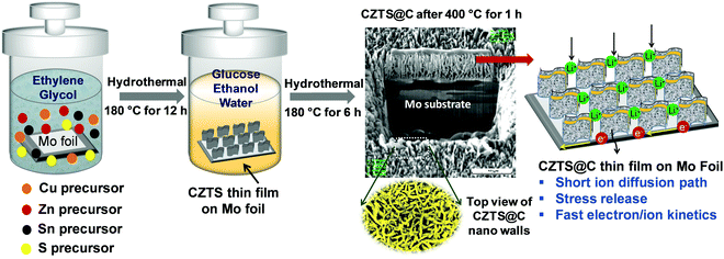 |
| | Scheme 1 Synthesis of CZTS@C films on a Mo substrate. | |
2.3. Material characterizations
Small pieces with a size of 10 mm × 10 mm were cut from the as-prepared CZTS thin-film nanostructure samples. The effective mass of CZTS thin film deposited on Mo substrate is ∼0.3–0.8 mg. The crystal structure of CZTS thin film before and after LIBs cycling processes were studied by X-ray diffraction (XRD) (Bruker D8) with Cu Kα radiation. The surface morphology of CZTS and CZTS@C thin films was investigated using field emission scanning electron microscopy (FE-SEM, JSM-6500) with an energy-dispersive X-ray (EDX) analyser. Microstructure and elemental distribution of CZTS@C thin-film were analysed using high-resolution transmission electron microscopy (HRTEM, JEOL2000FX) with an FEI Tecnai G2 electron microscope-coupled X-ray energy dispersive spectrometer (EDS, BRUKER AXS). The XPS technique is used to find the oxidation state of carbon-coated CZTS constituting elements with monochromatic Al Kα source (1486.6 eV) operated under ultra-high vacuum and analyzed by XPSPEAKS41 software, all the binding energy peak positions were calibrated by the C 1s peak 284.6 eV. The carbon amount in CZTS@C was analysed by the elemental analysis (EA) technique. Raman measurements were also performed to understand the detailed carbon coating information on CZTS at different carbon coating conditions.
2.4. Surface characterization of cycled electrodes
Field emission scanning electron microscopy (FE-SEM, JSM-6500) was used to study the surface morphology of CZTS and CZTS@C before and after cycling. In addition, scanning electron microscopy (SEIKO SMI3050SE Modular Cross Beam workstation, equipped with a focused ion beam, FIB) was also used to examine the cross-section images of CZTS and CZTS@C electrodes before and after long term cycling. Before the SEM analysis, the coin cells were de-assembled in an argon-filled glovebox (H2O and O2 content <0.1 ppm) and washed cycled electrodes with dimethyl carbonate (DMC) to remove the residual amount of electrolyte solvent on the electrode surface.
2.5. Electrochemical measurements
The electrochemical performances of the prepared CZTS thin films were measured in a coin cell (CR2032) assembled in an argon-filled glove box. The as-prepared CZTS thin-film samples on Mo substrate were chosen as the working electrodes, lithium metal foils as the counter electrodes, a polypropylene film (Celgard 2325) as the separator, and 1.0 M LiPF6 mixed with ethylene carbonate, dimethyl carbonate and diethyl carbonate (EC/DMC/EMC + 1% VC, 1:1:1 + 1% VC in volume) as the electrolyte. The electrolyte volume added to each cell was 40 microlitres. After the cells were shelved for ∼12 h, galvanostatic charge/discharge tests were conducted using a battery tester (AcuTec Systems, Taiwan) with a voltage range of 5 mV–3 V. Herein, every cell was tested at various C-rates and achieved reproducibility more than three times. Cyclic voltammetry (CV) tests were performed on the Solatron electro-voltammetry workstation in the voltage range 5 mV to 3.0 V at a scanning rate of 0.5 mV s−1. Electrochemical impedance spectroscopy (EIS) was performed on cycled electrodes on a PARSTAT MC multi-channel electrochemical workstation with an amplitude potential of 10 mV and a frequency range of 0.01 Hz to 1 MHz. All electrochemical tests were conducted at room temperature. After cycling performance, cells were disassembled under an argon-filled glove box and CZTS electrodes were washed with DMC solutions to remove electrolytes for further characterization.
3. Results and discussion
3.1. Structural and morphological studies
The carbon-coated CZTS thin films of different thicknesses were fabricated by a two-step hydrothermal process. The phase identification of the carbon-coated CZTS samples was performed from powder X-ray diffraction patterns as shown in Fig. 1a. From XRD patterns, diffraction peaks at 2θ = 28.4, 47.3 and 56.4 of carbon-coated CZTS samples were corresponding to (112) and (220) lattice planes of CZTS, and the structure matched well with the kesterite structure of CZTS (JCPDS no. 26-0575).18,22 Moreover, there is no information for specific crystalline carbon peaks in all carbon-coated CZTS samples, indicating that the carbon has been reduced, and as well existing in an amorphous form. Besides, there is a broad peak at around 26.96° (2θ) was observed for all samples, revealing the (100) plane of metastable wurtzite CZTS. The observed metastable wurtzite CZTS peak intensity gradually increases with the increase in the thickness of the CZTS film. The 100 plane corresponding to CZTS peak evolution is well-matched with previous reports.22 Similar kinds of diffraction peaks were observed in the case of pure CZTS thin films [see in Fig. S1, ESI†]. In order to confirm the phase purity of all the prepared CZTS thin-film samples and to find out the quality of carbon layer coating over CZTS, Raman spectroscopy was performed and the data is shown in Fig. 1b. The observed major intense peak at around 335 cm−1 for all carbon-coated CZTS thin-film samples corresponded to the A1 symmetry revealing vibrations of the S atom in the single-phase kesterite structure of CZTS.23 Additionally, Raman spectra of corresponding samples A, B and C showed characteristic G and D bands at 1585 and 1355 cm−1 revealing sp2 graphitic carbon and sp3 disordered carbon from the carbon coating of CZTS@C.24 The high intensity of the G band in the Raman spectra represents graphitic carbon-rich layer coated on CZTS films and may aid to improve electronic conductivity as well as the buffer the volume expansion.
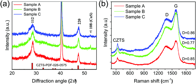 |
| | Fig. 1 (a) XRD and (b) Raman spectra for carbon-coated CZTS thin-films deposited on Mo substrate at different time intervals. | |
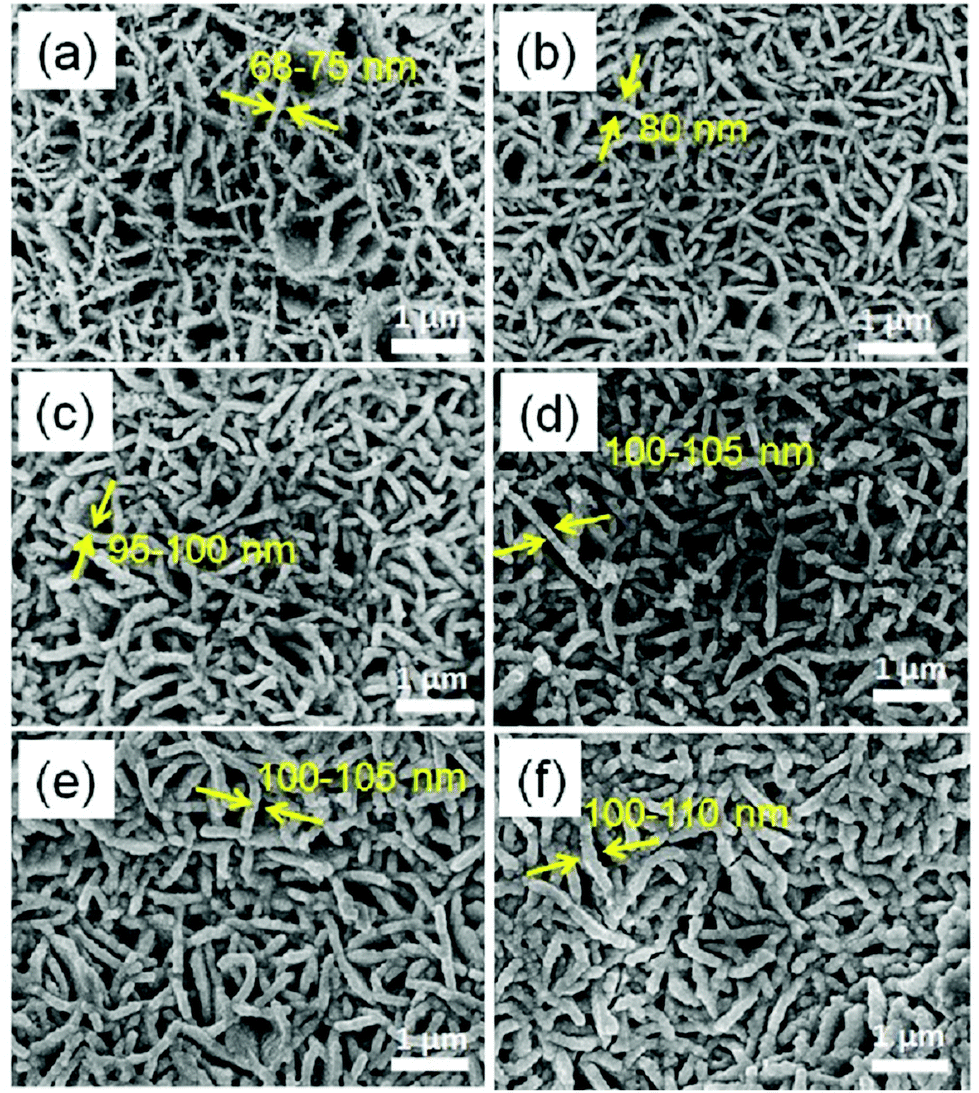
SEM analysis was performed to study the morphology of pure CZTS and carbon-coated CZTS thin films, and the data are shown in Fig. 2. The cross-sectional SEM images of carbon-coated CZTS samples can also be seen in Fig. S2 [see in ESI†]. From SEM images, we can observe CZTS is in the nanowall structure, and they are interconnected with wall thickness in the range of 75–105 nm, as shown in Fig. 2a, c and e. After carbon coating, CZTS nanowall thickness slightly increases to around 3–5 nm, as seen in Fig. 2b, d and f. From SEM images, the CZTS@C nanowall structure with very thin carbon-coating endows the material with short diffusion pathways and is easier for Li+/electron transportation for enhanced electrochemical performance.
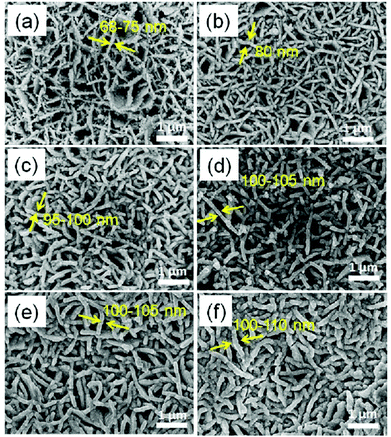 |
| | Fig. 2 SEM images of (a, c and e) CZTS thin film samples A1, B1 and C1, (b, d and f) corresponding carbon-coated CZTS thin film samples A, B and C, respectively. | |
The detailed morphology, crystallographic structure together with the elemental distribution of sample A were analysed using high-resolution transmission electron microscopy. As shown in Fig. 3, from the HRTEM image, we observed that the entire CZTS surface was uniformly coated with carbon with around 3 nm thickness, as shown in Fig. 3a. The carbon content measured from EA is around 4.5 wt% [see ESI† in Table S1], we believe that the obtained uniform carbon-coating can enhance the conductivity of the CZTS electrode to achieve faster rate kinetics. From the cross-sectional image of sample A in Fig. 3b, the CZTS thin film was deposited on the Mo substrate with a thickness of 1.7 μm, and CZTS nanowalls are well interconnected (see in Fig. 3c). The tightly interconnected structures revealed good mechanical properties as well as fast electronic transport between the tightly connected CZTS nanowalls. Further, the pore size distribution in the CZTS film (see in Fig. 3d) can facilitate the penetration of electrolytes easily, shorten the lithium ion diffusion pathways, and it can help in controlling volume expansion problems during the lithiation–delithiation process. The HRTEM image clearly showed lattice fringe with an interplanar spacing of 0.315 nm and 0.19 nm as the (112) and (220) crystal planes, respectively, of kesterite CZTS (PDF-26-0575) as shown in Fig. 3e. These results are in good agreement with the selective area electron diffraction (SAED) pattern (see Fig. 3f) as well as XRD results.18,21 From TEM and XRD results, we believe that CZTS films with high-quality nanocrystals and smaller grains can be successfully prepared by a solution-based low-cost hydrothermal method. The additional EDS spectrum of particle region (in Fig. 3g) confirms the presence of Cu, Zn, Sn, S and C elements (see ESI† in Fig. S3). The corresponding EDS elemental mapping results in Fig. 3(h–l) demonstrated that five elements, such as Cu, Zn, Sn S, and C were homogeneously distributed in the CZTS system.
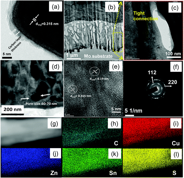 |
| | Fig. 3 TEM images of sample A (a) HR-TEM image of carbon film with CZTS (b and c) cross-section image (d) pore size distribution (e) HR-TEM images (f) SAED (g–l) TEM image and the corresponding C, Cu, Zn, Sn and S elemental mapping images of sample A, respectively. | |
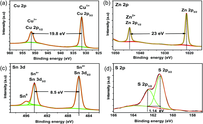
Furthermore, X-ray photoelectron spectroscopy (XPS) measurement is also used to confirm the expected oxidation states of elements in sample A (CZTS@C). After careful fitting, the copper 2p peaks located at 932.03 and 951.78 eV with a peak separation of 19.76 eV, representing Cu (1+) state (see in Fig. 4a), and is in good agreement with the standard separation energy gap 19.9 eV state for all CZTS based samples.25,26 Zn spectrum core-level peaks 2p3/2 and 2p1/2 of sample A were positioned at 1021.3 and 1045.1 eV with peaks splitting of 23 eV, respectively, indicating Zn (2+) state (Fig. 4b) for all sulfurized samples.26,27 The binding energies of Sn 3d5/2 and 3d3/2 core level peaks at 486.0 and 494.48 eV, respectively, with a peak separation of 8.45 eV, corresponding to Sn (4+) state (see in Fig. 4c).28 Moreover, we found a smaller shoulder peak at 495.23 eV from SnO2 due to the partial oxidation of Sn during the synthesis process. However, the obtained SnO2 peaks of sample B could not be confirmed from XRD due to either it is minimal or in the amorphous form. On the other hand, sulphur 2p spectrum core-level peaks were located at 161.31 and 162.5 eV with an energy gap separation of about 1.14 eV, and another peak was observed at 163.74 eV, all these peaks are consistent with the sulphide phases of S in the range from 160 to 164 eV (Fig. 4d).21,25
 |
| | Fig. 4 High-resolution Cu 2p, Zn 2p, Sn 3d, and S 2p XPS spectra of sample A. | |
3.2. Electrochemical performance studies
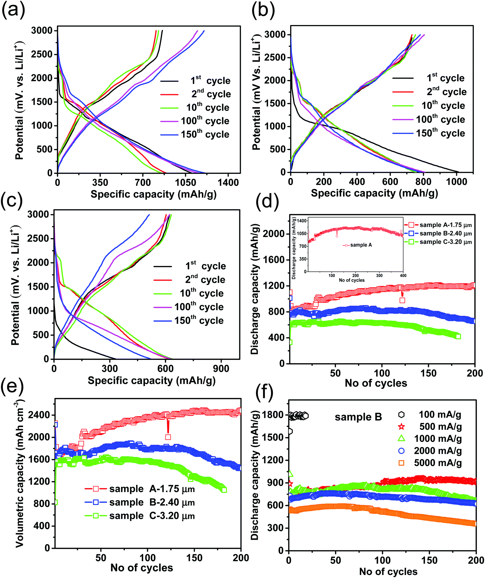
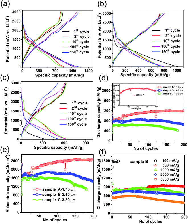
In order to understand the lithium-ion storage behaviour for different thicknesses of samples, electrochemical charge/discharge voltage profiles of the pure CZTS and CZTS@C samples were tested at a current density of 1000 mA g−1 in the potential range from 0.005 to 3 V. The complete charge/discharge profiles of samples A, B and C are shown in Fig. 5(a–c). From charge/discharge profiles, all CZTS@C samples from the 2nd to 10th cycle possess a major steep discharge curve at 1.2 V and 0.5 V, which are associated with Li–Sn and Li–Zn alloy, respectively.18,19 In the charging process, the observed charge plateau at 2.2 V is mainly attributed to the reversible reaction for Cu1−xS materials in CZTS@C. Meanwhile, the above-mentioned voltage plateaus of pure CZTS samples are slightly disappeared especially after the 10th cycle [see ESI† in Fig. S4], which represented partial reversibility of pure CZTS. Even after 100 cycles, the reversibility of all CZTS@C thin-film samples exhibited almost similar behaviour, but it is completely disappeared in pure CZTS samples. The electrochemical charge/discharge voltage profiles clearly represented that carbon-coating could successfully control the volume expansion problems and maintain the reversibility of CZTS, and thereby improve the cyclic performance during the lithiation–delithiation process.24 The cyclic performances of all samples are demonstrated in Fig. 5d. Herein, CZTS@C samples with different film thicknesses have a great impact on cyclic performance compare to pure CZTS samples. Among those, sample A showed a high initial discharge capacity around 1100 mA h g−1 and charge capacity of 860 mA h g−1 with coulombic efficiency of 78%, and eventually, it increases to 99–100% with progressive cycling as shown in Fig. S5 (ESI†). Besides, its discharge capacity slightly increases from 25 cycles to 150 cycles due to the gradual activation of metal sulfide electrodes as well as the charge plateau at ∼2.35 V (Fig. 5a). The discharge capacity of sample A becomes stable from 150th cycle to 300 cycles and then decreases slowly from 300 to 450 cycles, see inset figure in Fig. 5d.29 Interestingly, sample B with a higher thickness also showed excellent capacity retention, i.e., above 85% over 200 cycles as shown in Fig. 5d. On the other hand, sample C exhibited low discharge capacity as compared to samples A and B. The gradual decaying cyclic performance of sample C after 150 cycles is due to uncontrolled volume expansion problems of thicker electrodes during the lithiation/delithiation process. Further, we measured volumetric capacities of all CZTS@C samples as shown in Fig. 5e. Based on tap densities of all samples, the volumetric capacities were estimated to be around 2470, 1726 and 1300 mA h cm−3 for samples A, B and C, respectively (see ESI† for calculation details). The calculated volumetric capacity of the CZTS@C anode is almost 4–6 times higher than that of commercial graphite anodes (441 mA h cm−3).30 Impressively, it is even higher than recently reported Si anodes,31–33 but lower than the volumetric capacity of Si–CNT film.34 The mass loading of CZTS thin-film plays an important role in practical micro battery applications. The CZTS mass loading in this present study is in the range of around 0.35–0.8 mg cm−2, which is higher than that in previous reports.18,20,35 We noted that the typical anodic mass loading amount of 0.5–0.8 mg cm−2 is used in this present study, which may meet practical microbattery applications. Based on comparable areal capacity and stability performance, sample B was chosen for the stability test at different current rates and compared with the rate capability test. In the electrochemical battery performance, sample B reveals a high and stable discharge capacity around 925, 655, 625 and 351 mA h g−1 even after 200 cycles at current densities 500, 1000, 2000 and 5000 mA g−1, respectively, as shown in Fig. 5f. The observed discharge capacity performance is well consistent with the rate capability test results [see ESI† in Fig. S5]. Meanwhile, for comparison studies, we carried out a cyclic performance test for pure CZTS samples [see ESI† in Fig. S4], and observed that their capacity was quickly fading with the progressive cycling process due to the uncontrollable volume expansion problems during charge/discharge. The areal capacity also is another important factor for commercial LIB's applications. In the present work, the areal capacity of the thicker electrode (sample C – thickness 3.2 μm) delivered a high areal capacity of around 0.51 mA h cm−2 after 100 cycles at high current density 0.8 mA cm−2 [see ESI† shown in Fig. S5]. However, the areal capacity of sample C decreases gradually after 150 cycles as compared to other electrodes (sample A – thickness 1.75 μm and sample B – thickness 2.4 μm). The improved cyclic performance and volumetric capacities of CZTS@C electrode are due to the uniform carbon coating, which could successfully enhance the conductivity as well as controlled the crack pattern formation of the CZTS electrode will be discussed in the later section.
 |
| | Fig. 5 (a–c) Charge and discharge profiles (d) cyclic performance at a current density 1000 mA g−1 (e) corresponding volumetric capacities of carbon-coated CZTS samples A, B and C, respectively (f) cyclic performance of sample B at various current densities. | |
3.3. Morphological evolution after cycling
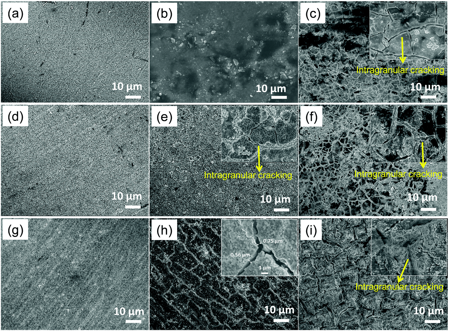
The cracking behaviour of thin-film was studied by SEM to better understand the reversible capacity fading for different thicknesses of both CZTS@C and CZTS after selected cycles as shown in Fig. 6. The SEM analysis shows that all CZTS@C films are free from cracks before cycling (Fig. 6a, d, g for 1.75 μm, 2.48 μm and 3.42 μm, respectively). However, the growth of cracks progressively increased with an increase of CZTS thin-films thickness as well as the cycle number regardless of film thickness (shown in Fig. 6c, e, f, h, and i). Especially for the thinner electrode (sample A – 1.75 μm film thickness), there is no crack pattern formation after 10 cycles, but the thin layer became fine cracks and dense after 100 cycles as compared with other films, and it is in good agreement with previous reports.9,36 Although, the behavior of the crack pattern formation is still observed in highly porous and less dense CZTS@C thin-film anode, however, the generation of cracks are well controlled due to the carbon coating on the top of CZTS and form intra-granular cracks at a deeper level and are strongly connected with the substrate. Interestingly, we observed a high density of intra-granular cracks on the electrode surface, inducing more active sites on the surface for lithium storage that enhanced capacity from 10 cycles to 100 cycles. Moreover, intra-granular cracks diffuse electrolytes easily among the active particles and shorten the lithium-ion diffusion length, which reveals excellent stability of up to 350 cycles.37 Therefore, carbon coating over the CZTS surface could successfully control the crack pattern formation during the lithiation/de-lithiation process over cycling. On other hand, in pure CZTS (sample A1), the evolution of deep cracks takes place immediately after 10 cycles and is gradually separated into isolated Islands after 100 cycles due to the severe uncontrolled volume expansion problems during the charge/discharge process. From a higher magnification SEM image of the deep crack on the electrode surface (inset) in Fig. S6(b) (ESI†), we observed that there is around a 1 μm gap between the islands. The observed huge volume expansion-induced severe cracking patterns on the electrode surface revealing the instability of LIB anode during cyclic performance. The volume expansion-induced deep crack pattern formation on the surface of anode possesses (1) poor grain-to-grain connections, (2) leading electrical disconnection between the particles, (3) loss of active sites due to structural disintegration; (4) forming new surfaces on the electrode substrate, and finally (5) react with electrolyte, where it is decomposing and forms an insulating layer between the current collector and active materials that isolated CZTS grains from the substrate. Additionally, deep crack pattern formation decays the stability of the electrode gradually over the cycling process in LIB [see ESI† in Fig. S4]. Moreover, the observed cracks in pure CZTS are well consistent with those in other anode materials such as Si, Ge and Sn thin films, where severe cracks pattern formation leading to fast capacity fading, which occurs with the film thickness of above 1 μm.9,17,37 Although, the evolution of intra-granular cracks takes place after 100 cycles in sample B (thickness 2.4 μm), they are still strongly connected with the current collector similar to sample A, as shown in Fig. 6f. Meanwhile, sample C (3.2 μm film thickness) generates cracks from 10 cycles onwards (see in Fig. 6h), and it is gradually becoming big branches after 100 cycles. Even though cracks appear between grains at the surface level, but they are still interconnected with each other at a deeper level, see inset figure in Fig. 6(f and i), and it caused minute capacity decay after 100 cycles (see Fig. 5d). Based on SEM images of all cycled electrodes, it is concluded that the generation of cracks on the CZTS@C thin films surface is well controlled and it creates new active sites for lithium storage as compared with pure CZTS. Moreover, the moderate generation of cracks from cycled electrodes of carbon-coated samples maintained the CZTS@C phase, but severe crack pattern formation in pure CZTS collapses their crystallinity [see supporting information in Fig. S8, ESI†].
 |
| | Fig. 6 SEM images of as-deposited (a, d and g) CZTS thin film samples A, B, C, and (b and c) cycled electrode of sample A, (e and f) cycled electrode sample B, (h and i) cycled electrode of sample C after 10th and 100th cycle was charged to 3 V. | |
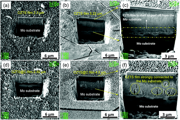
3.4. Study of volume expansion and electrode stability after cycling
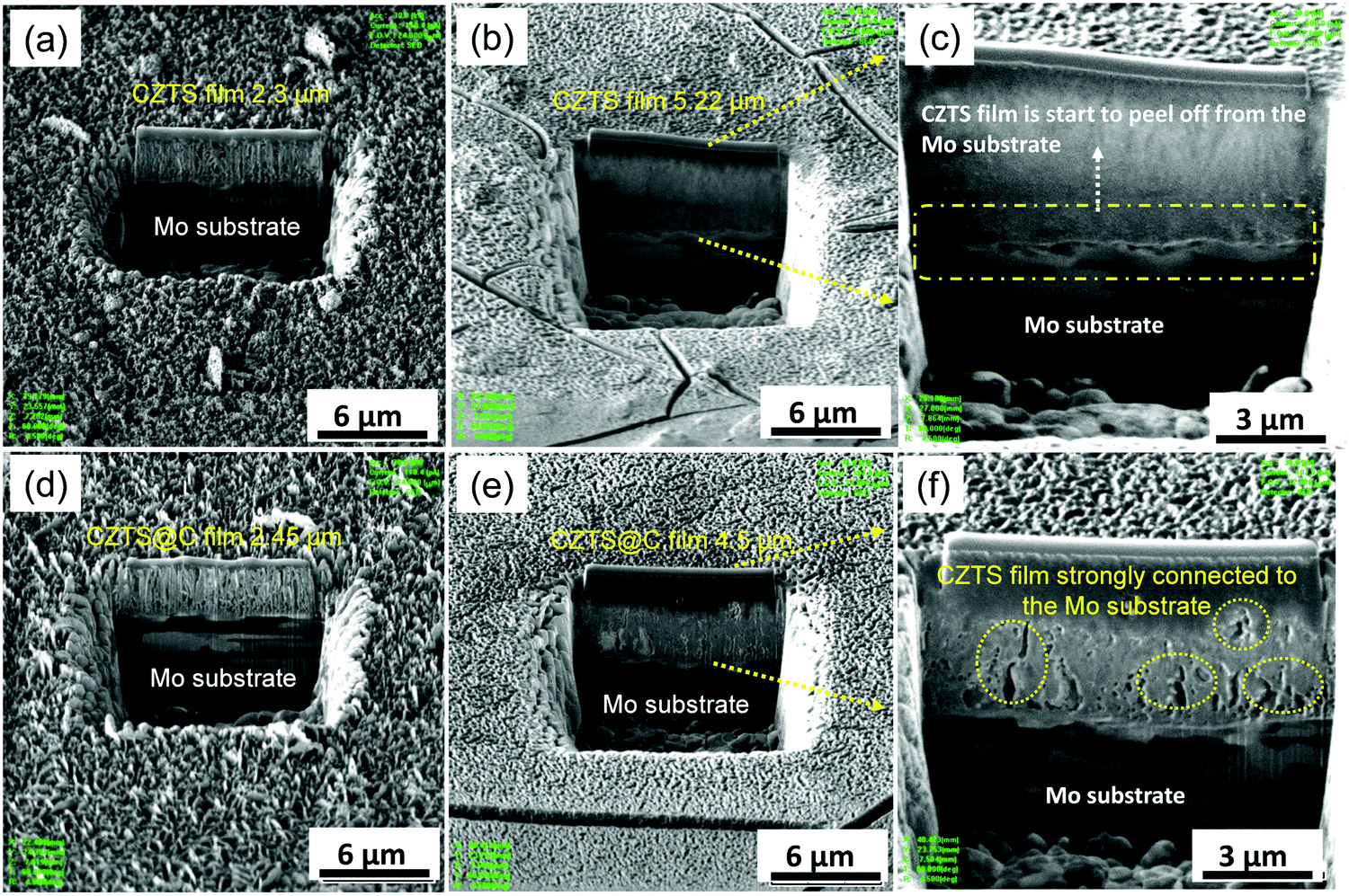
Fig. S7 (ESI†) and Fig. 7 show top view and cross-sectional SEM micrographs of sample B1 (CZTS-2.3 μm) and sample B (CZTS@C-2.45 μm) electrodes before and after 100 cycles. The pristine CZTS shows a homogenous porous structure as shown in Fig. S7 (ESI†). Unexpectedly, after 100 cycles, the repeated lithiation/de-lithiation process over cycling possesses CZTS volume expansion/contraction issues, and it is leading to the creation of cracks at a deeper level as well as small island formation takes place (see in marked circles in Fig. S7, ESI†). Thereafter, the electrolyte can easily pass through these deeper cracks on the surface of the electrode, and it further decomposes, leading to the formation of thicker SEI in between the porosity of CZTS particles as well as at the interfaces of bare CZTS/electrolyte and CZTS/Mo substrate. As a result, the porosity of CZTS disappears and electrode thickness increases to 5.22 μm, as also clearly observed at cross-sectional SEM micrographs in Fig. 7b, and eventually, it is starting to peel off from the Mo substrate (see Fig. 7c). Consequently, the thicker SEI layer blocking lithium-ion transport as well as responding to the electrical disconnection between CZTS particles, causing decaying of the stability of sample B1 electrode slowly over cycling. On other hand, the sample B electrode film thickness increases to 4.5 μm after 100 cycles, as shown in Fig. 7e. Here, the evolution of shallow cracks mainly takes place only at the surface level and the formation of islands was totally controlled because of carbon coating is as shown in Fig. S7 (ESI†). Moreover, the availability of pores on the surface of electrodes (see marked circles in Fig. 7f) can easily allow the electrolyte and enhance the reaction kinetics over cycling. Therefore, the structure and integrity of sample B electrode are maintained, which is strongly attached to the Mo substrate even after 100 cycles (see in Fig. 7f). From these investigations, it is revealing that the volume expansion of sample B1 is about 225%, while sample B electrode performs only 185% after 100 cycles. Interestingly in the present work, the alloying reaction (below 1 V) and conversion reaction mechanism (above 1 V) in the CZTS system are involved in the crack pattern formation, which is different from other anode systems such as alloying reactions based on Si and SnO2 as well as the conversion reaction based on MoS2 and SnS2. It has been reported that mostly the alloying reaction-based anodes undergo huge volume expansion problems during cycling, for example, silicon has more than 400% volume change for Li3.75Si38 and SnO2 around 300% volume change for Li4.4Sn.13 The huge volume expansion induced the pattern of a severe crack on the electrode surface, which reveals the electrical disconnection between the active particles, and thus it causes instability of LIB anodes during cyclic performances. Interestingly, in the case of the CZTS system, the evolution of cracks well controlled the volume expansion of CZTS@C around 185% as compared with the pure CZTS (225%) during the cycling process. We believe that in CZTS, the formation of metals such as Cu and Zn during the cycling process primarily leads to enhanced conductivity of the electrode and finally facilitating adsorption of Li+ despite the crack pattern formation during cycling.21 Thus, we believe that CZTS can be a promising choice as a high-performance anode material for next-generation lithium-ion battery applications.
 |
| | Fig. 7 FIB cross-sectional micrographs of pristine sample B1 (a) before (b and c) after 100 cycles and sample B (d) before cycling (e and f) after 100 cycles. | |
3.5. Cyclic voltammetry studies
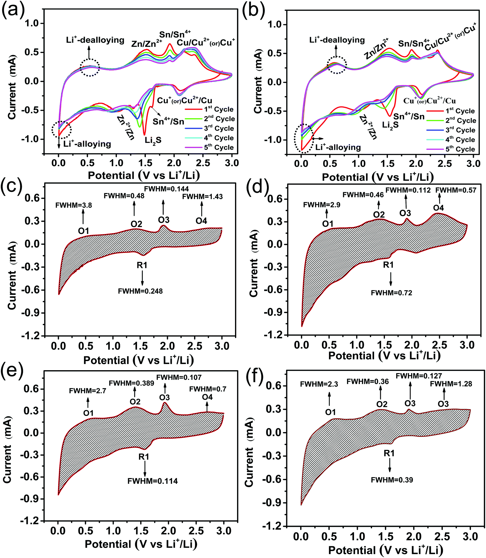
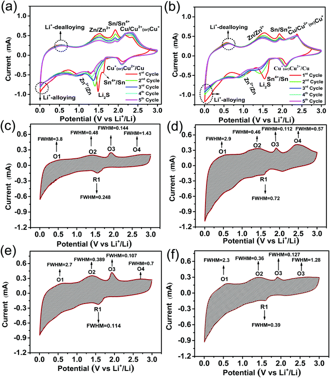
In order to investigate the lithium storage reaction mechanism, the cyclic voltammogram (CV) was carried out for the sample A1 and A. Fig. 8a and b shows the specific CV profiles for the first five cycles of sample A1 and A in the potential range from 0.005 V to 3 V at a scan rate of 0.5 mV s−1. The cyclic voltammogram reveals characteristic four broad reduction peaks during the cathodic scan upon the first lithiation, which is similar to the reported metal sulphide electrode behaviour. Specifically observed, first reduction peaks at around 2.1 V, correspond to the lithiation of Li–CuxS alloys, and other two peaks around 1.4–1.5 and 1.1 V are mainly ascribed to the multistep reactions of Sn and Zn species as well as the formation of a solid electrolyte interface (SEI).19,39–41 Furthermore, the observed final reduction peak at around 0.4–0.5 V is ascribed to the conversion reaction between Sn and Zn.19 Whereas, in the anodic scan of sample A1, four oxidation peaks at around 0.55, 1.5, 1.9 and 2.34 V are observed, in which the peak at ∼0.55 V is related to the de-lithiation of Sn and Zn alloy, and the peaks at 1.5 and 1.9 V are related to the reversible reactions between Sn, Zn, and Li. The observed broad peak from 2.3 to 2.4 V can be assigned to delithiation of Li–CuxS alloys and oxidation of Li2S to S and lithium ions.41–43 Sample A also followed a similar electrochemical reaction mechanism in sample A1, as shown in Fig. 8b and its good match with our expectation. Moreover, CV curves of sample A at the 2nd, 3rd, 4th and 5th cycles are coinciding very well with each other as compared with sample A1, indicating that carbon coating could successfully control the growth of the SEI layer formation during the electrochemical cycling process.44,45 Even after 100 cycles, CV results of three electrodes (Fig. 8d–f) demonstrated that the reversibility of CZTS is maintained very well because of carbon coating. On other hand, the reversibility of pure CZTS (see in Fig. 8c) is diminished due to the crack pattern formation from volume expansion problems during cycling. Furthermore, after the calculation of FWHM values of both the oxidation (O1) and reduction (R1) peaks of the pure CZTS and carbon-coated CZTS samples, it is found that the FWHM values of oxidation peaks were smaller in the case of carbon-coated CZTS samples. Hence, it indicates that the carbon coating could not only accelerate the electrode reaction but also improved lithium storage in CZTS as compared with pure CZTS.46 Overall, CV results demonstrated the progressive development of cracks in pure CZTS resulting in sluggish electrode reactions after 100 cycles. Interestingly, in CZTS@C samples, carbon coating not only controls the crack pattern formation but also improves the electronic conductivity of CZTS, together with moderate stability of the CZTS electrode, which has been discussed in the previous section.
 |
| | Fig. 8 Cyclic voltammogram for (a) sample A1 (b) sample A for the first 5 cycles, and (c–f) after 100 cycles for sample A1, sample A, sample B and sample C. | |
Based on the above electrochemical performance, we anticipate the following microstructure evolution upon lithiation/delithiation during cycling, as shown in Fig. 7, pure CZTS nanostructure suffers from severe volume expansion upon lithiation/delithiation during cycling, and finally the relatively large size LixCZTS makes it vulnerable to cracking at a deeper level [see ESI† in Fig. S6]. These severe deep crack pattern formations reveal the collapse of CZTS morphology after 100 cycles see in Fig. 9(a and b). Finally, the deep crack pattern formations (Fig. S6, ESI†) cause the collapse of CZTS morphology after 100 cycles, as shown in Fig. 9(a and b). Eventually, the deterioration of the film from the substrate (Fig. 7c) reveals the increased charge transfer resistance (Fig. S9, ESI†) and sluggish electrochemical kinetics as cyclic voltammetry as shown in Fig. 8c, and by which, stability of pure CZTS electrode failed gradually over cycling. In CZTS@C thin-film, the intra-granular cracks propagating radially from surface level due to carbon coating, which controlled the volume expansion (see in Fig. 6c, f, i and Fig. S7, ESI†). Hence, we observed that the reactive species of LixCZTS@C maintained their morphology and crystal structure even after 100 cycles, as shown in Fig. 9(b and c). Moreover, based on the above observations, CZTS@C possesses an extraordinary electrochemical performance even at higher current rates as compared to other literature reports, as shown in Fig. 9d.
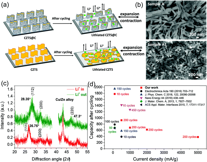 |
| | Fig. 9 (a) Schematic illustration for structure changes after cycling (b) morphology evolution after 100 cycles (c) XRD of sample A after 100 cycles (d) comparison of electrochemical performance of our work with other literature reports. | |
3.6. Electrochemical impedance spectroscopy studies
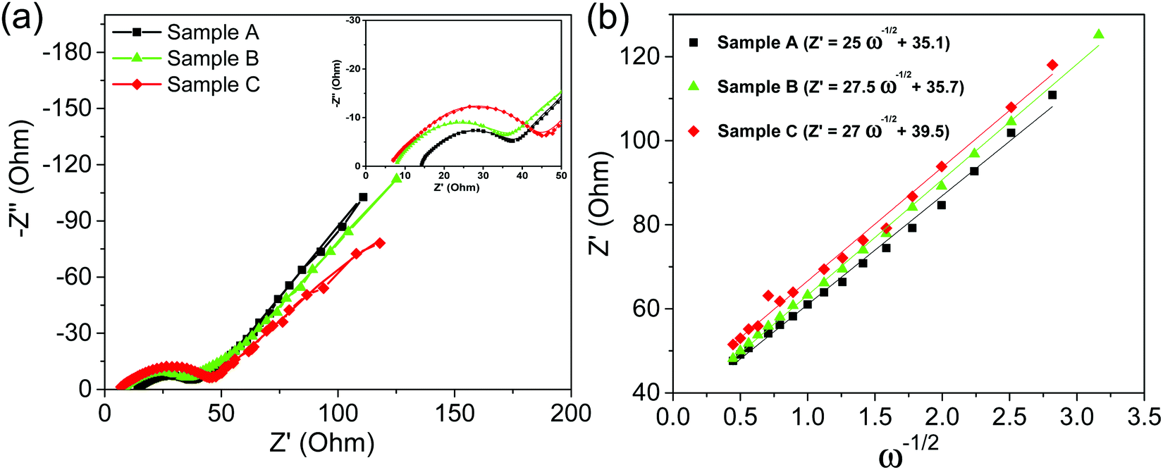
Finally, in order to study the effect of cracks formation over charge transfer resistance of CZTS and CZTS@C, EIS was carried out on all cycled electrodes as shown in Fig. 10(a and b). EIS spectra show two characteristic semi-circles in the high-frequency region and an inclined straight line in the low-frequency range. The three impedance spectra of sample A, B, C coin cells show similar features: a medium-to-high-frequency depressed semicircle and a low-frequency inclined line, which is well consistent with previous sulphur-based materials. The observed first semicircle at the high-frequency region represents contact resistance (Rf) and resistance of Li+ ion's transfer through the SEI layer (RSEI) and the second semicircle at the medium-frequency region represents the charge-transfer resistance (Rct) at the interface between the electrode and electrolyte.47 The inclined straight lines in the low-frequency section are corresponding to the Warburg impedance (Zw), which is related to the diffusion of Li+ ions within the electrode.48,49 After fitting EIS spectra, we found that charge transfer of CZTS@C samples (see in Fig. 10a) was enhanced compared with pure CZTS samples [see ESI† in Fig. S9 and fitted EIS parameters in Table S2]. We believe that the carbon coating could successfully have enabled CZTS to improve the charge transfer at the electrode–electrolyte interface via intragranular crack formation, which is responsible for fast reaction kinetics. Furthermore, the inclined lines of the low-frequency region in the EIS spectra were corresponding to the Warburg impedance (Zre) is related to Li+ ion diffusion in the active material.50 At the low-frequency region of the Nyquist plot, an almost vertical straight line was observed for carbon-coated CZTS samples as compared with pure CZTS samples; which revealed that an ultra-thin carbon coating over CZTS particles enabled improved electrical conductivity and ion transfer during the controlled crack formation of CZTS@C, thus leading to the enhancement of Li+ diffusion into the inner spaces of the electrode materials. The lithium-ion diffusion coefficient can be calculated from the following equations below.50,51| | 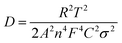 | (1) |
| | | Zre = Rct + Re + σω−1/2 | (2) |
where D is the diffusion coefficient of Li+, R is the gas constant, T is the absolute temperature, C is the concentration of Li+ in the electrode, n is the number of electrons transferred during the reaction, F is the Faraday constant, A is the surface area of the electrode, and σ is the Warburg factor. Based on above eqn (2), the Warburg factor can be obtained from the slope between Zre and ω−1/2 plots (see in Fig. 10b), which can provide insight into the charge kinetic behaviour in CZTS@C electrodes.52 By keeping C as a constant in eqn (1), the results demonstrated that it is almost the same Li-ion diffusion coefficient value for all CZTS@C electrodes, and is higher compared with pure CZTS (see ESI† in Fig. S9). Based on the above results, the CZTS@C electrodes possess better ionic conductivity from controlled crack pattern formation than pure CZTS. Hence, as we expected, the improved conductivity, ion transfer and enhanced Li+ diffusion resulted in better rate capability and long cyclic performance for carbon-coated CZTS thin-film electrodes.
 |
| | Fig. 10 (a) Nyquist plots of sample A, sample B and sample C after 100 cycles, and (b) their corresponding linear fitting between Zre and ω−1/2 in the low-frequency region. | |
4. Conclusion
The interconnected nanowalls of CZTS@C thin-films prepared using the hydrothermal method exhibited high lithium-ion storage through microstructural intra-granular cracks. In the present work, a systematic microscopic and electrochemical study has been carried to understand the effect of crack formation upon LIB electrochemical performance for pure CZTS and carbon-coated CZTS samples, respectively. The islands of pure CZTS formed during the repeated cycling are leading to a severe capacity decay over cycling. On the other hand, the uniform carbon coating on the CZTS surface plays a major role in controlling crack's pattern formation and maintains the reversibility of CZTS, which could lead to high volumetric capacity 2477, 1726 and 1300 mA h cm−3 and gravimetric capacity 1210, 785 and 520 mA h g−1 for different thicknesses of CZTS@C films at the current density 1000 mA g−1 after 150 cycles. Among them thinner electrodes showing high capacity from 1210–970 mA h g−1 over 400 cycles. Further, post-SEM analysis reveals that intra-granular cracking formation from repeated lithiation and delithiation is enhanced electrochemical kinetics of carbon-coated CZTS thin-films in subsequent cycles, and this argument is well supported by CV and EIS studies. We strongly believe that a better understanding of critical island and control-cracking mechanisms of different thicknesses is urgently needed for designing high-performance anodes for next-generation lithium-ion batteries.
Conflicts of interest
The authors declare that they have no known competing financial interests or personal relationships that could have appeared to influence the work reported in this paper.
Acknowledgements
We thank the Ministry of Science and Technology (MOST 107-2113-M-001-010-MY3 and MOST 109-2124-M-001-004), Academia Sinica, National Taiwan University, and the Ministry of Education (MOE) of Taiwan for financial support. A joint project between Academia Sinica and the Industrial Technology Research Institute (ITRI) and technical support from the Nano Core Facility of Academia Sinica (Taiwan) are also acknowledged.
References
- J. B. Bates, N. J. Dudney, B. Neudecker, A. Ueda and C. D. Evans, Solid State Ionics, 2000, 135, 33–45 CrossRef CAS.
- C. K. Chan, H. Peng, G. Liu, K. McIlwrath, X. F. Zhang, R. A. Huggins and Y. Cui, Nat. Nanotechnol., 2008, 3, 31–35 CrossRef CAS PubMed.
- J. Zhang, T. Huang, Z. Liu and A. Yu, Electrochem. Commun., 2013, 29, 17–20 CrossRef CAS.
- X. Zhou, L. J. Wan and Y. G. Guo, Adv. Mater., 2013, 25, 2152–2157 CrossRef CAS.
- A. M. Gaikwad, B. V. Khau, G. Davies, B. Hertzberg, D. A. Steingart and A. C. Arias, Adv. Energy Mater., 2015, 5, 1401389 CrossRef.
- L. Liu, F. Xie, J. Lyu, T. Zhao, T. Li and B. G. Choi, J. Power Sources, 2016, 321, 11–35 CrossRef CAS.
- H. Tian, F. Xin, X. Wang, W. He and W. Han, J. Materiomics, 2015, 1, 153–169 CrossRef.
- G.-H. Lee, S. Lee, C. W. Lee, C. Choi and D.-W. Kim, J. Mater. Chem. A, 2016, 4, 1060–1067 RSC.
- J. P. Maranchi, A. F. Hepp, A. G. Evans, N. T. Nuhfer and P. N. Kumta, J. Electrochem. Soc., 2006, 153, A1246 CrossRef CAS.
- L. Y. Beaulieu, K. W. Eberman, R. L. Turner, L. J. Krause and J. R. Dahn, Electrochem. Solid-State Lett., 2001, 4, A137 CrossRef CAS.
- Y.-T. Cheng and M. W. Verbrugge, J. Appl. Phys., 2008, 104, 083521 CrossRef.
- X. H. Liu, H. Zheng, L. Zhong, S. Huang, K. Karki, L. Q. Zhang, Y. Liu, A. Kushima, W. T. Liang, J. W. Wang, J. H. Cho, E. Epstein, S. A. Dayeh, S. T. Picraux, T. Zhu, J. Li, J. P. Sullivan, J. Cumings, C. Wang, S. X. Mao, Z. Z. Ye, S. Zhang and J. Y. Huang, Nano Lett., 2011, 11, 3312–3318 CrossRef CAS PubMed.
- S. M. Hwang, Y.-G. Lim, J.-G. Kim, Y.-U. Heo, J. H. Lim, Y. Yamauchi, M.-S. Park, Y.-J. Kim, S. X. Dou and J. H. Kim, Nano Energy, 2014, 10, 53–62 CrossRef CAS.
- Q. Wu, B. Shi, J. Bareno, Y. Liu, V. A. Maroni, D. Zhai, D. W. Dees and W. Lu, ACS Appl. Mater. Interfaces, 2018, 10, 3487–3494 CrossRef CAS PubMed.
- I. Ryu, J. W. Choi, Y. Cui and W. D. Nix, J. Mech. Phys. Solids, 2011, 59, 1717–1730 CrossRef CAS.
- S. Pal, S. S. Damle, P. N. Kumta and S. Maiti, Comput. Mater. Sci., 2013, 79, 877–887 CrossRef CAS.
- M. Winter and J. O. Besenhard, Electrochim. Acta, 1999, 45, 31–50 CrossRef CAS.
- X. Yin, C. Tang, M. Chen, S. Adams, H. Wang and H. Gong, J. Mater. Chem. A, 2013, 1, 7927 RSC.
- J. Lin, J. Guo, C. Liu and H. Guo, ACS Appl. Mater. Interfaces, 2015, 7, 17311–17317 CrossRef CAS.
- G. Bree, H. Geaney, K. Stokes and K. M. Ryan, J. Phys. Chem. C, 2018, 122, 20090–20098 CrossRef CAS.
- J.-M. Chiu, T.-C. Chou, D. P. Wong, Y.-R. Lin, C.-A. Shen, S. Hy, B.-J. Hwang, Y. Tai, H.-L. Wu, L.-C. Chen and K.-H. Chen, Nano Energy, 2018, 44, 438–446 CrossRef CAS.
- B. Zhou, D. Xia and Y. Wang, RSC Adv., 2015, 5, 70117–70126 RSC.
- M. Zubair Ansari and N. Khare, J. Appl. Phys., 2015, 117, 025706 CrossRef.
- A. Ponrouch, A. R. Goñi, M. T. Sougrati, M. Ati, J.-M. Tarascon, J. Nava-Avendaño and M. R. Palacín, Energy Environ. Sci., 2013, 6, 3363 RSC.
- D. Tang, Q. Wang, F. Liu, L. Zhao, Z. Han, K. Sun, Y. Lai, J. Li and Y. Liu, Surf. Coat. Technol., 2013, 232, 53–59 CrossRef CAS.
- V. T. Tiong, Y. Zhang, J. Bell and H. Wang, CrystEngComm, 2014, 16, 4306–4313 RSC.
- X. Liu, Y. Hao, J. Shu, H. M. K. Sari, L. Lin, H. Kou, J. Li, W. Liu, B. Yan, D. Li, J. Zhang and X. Li, Nano Energy, 2019, 57, 414–423 CrossRef CAS.
- B. Venugopal, B. Nandan, A. Ayyachamy, V. Balaji, S. Amirthapandian, B. K. Panigrahi and T. Paramasivam, RSC Adv., 2014, 4, 6141 RSC.
- J. Lin, J. Guo, C. Liu and H. Guo, ACS Appl. Mater. Interfaces, 2016, 8, 34372–34378 CrossRef CAS PubMed.
- Q. Xiao, Y. Fan, X. Wang, R. A. Susantyoko and Q. Zhang, Energy Environ. Sci., 2014, 7, 655–661 RSC.
- T. Ma, X. Yu, H. Li, W. Zhang, X. Cheng, W. Zhu and X. Qiu, Nano Lett., 2017, 17, 3959–3964 CrossRef CAS PubMed.
- B. Wang, X. Li, T. Qiu, B. Luo, J. Ning, J. Li, X. Zhang, M. Liang and L. Zhi, Nano Lett., 2013, 13, 5578–5584 CrossRef CAS PubMed.
- S. Jeong, J. P. Lee, M. Ko, G. Kim, S. Park and J. Cho, Nano Lett., 2013, 13, 3403–3407 CrossRef CAS.
- X. Wang, L. Sun, R. Agung Susantyoko, Y. Fan and Q. Zhang, Nano Energy, 2014, 8, 71–77 CrossRef CAS.
- J.-M. Chiu, T.-C. Chou, D. P. Wong, Y.-R. Lin, C.-A. Shen, S. Hy, B.-J. Hwang, Y. Tai, H.-L. Wu and L.-C. Chen, Nano Energy, 2018, 44, 438–446 CrossRef CAS.
- J. Li, A. K. Dozier, Y. Li, F. Yang and Y.-T. Cheng, J. Electrochem. Soc., 2011, 158, A689 CrossRef CAS.
- B. Laforge, L. Levan-Jodin, R. Salot and A. Billard, J. Electrochem. Soc., 2008, 155, A181 CrossRef CAS.
- A. Reyes Jimenez, R. Klopsch, R. Wagner, U. C. Rodehorst, M. Kolek, R. Nolle, M. Winter and T. Placke, ACS Nano, 2017, 11, 4731–4744 CrossRef CAS PubMed.
- C. Zhai, N. Du, H. Zhang, J. Yu and D. Yang, ACS Appl. Mater. Interfaces, 2011, 3, 4067–4074 CrossRef CAS.
- Y. Jiang, Y. Feng, B. Xi, S. Kai, K. Mi, J. Feng, J. Zhang and S. Xiong, J. Mater. Chem. A, 2016, 4, 10719–10726 RSC.
- Q. Jiang, X. Chen, H. Gao, C. Feng and Z. Guo, Electrochim. Acta, 2016, 190, 703–712 CrossRef CAS.
- J. Zhou, J. Qin, X. Zhang, C. Shi, E. Liu, J. Li, N. Zhao and C. He, ACS Nano, 2015, 9, 3837–3848 CrossRef CAS PubMed.
- H. Wan, G. Peng, X. Yao, J. Yang, P. Cui and X. Xu, Energy Storage Mater., 2016, 4, 59–65 CrossRef.
- B. Wang, X. Li, X. Zhang, B. Luo, M. Jin, M. Liang, S. A. Dayeh, S. Picraux and L. Zhi, ACS Nano, 2013, 7, 1437–1445 CrossRef CAS PubMed.
- J. Qin, C. He, N. Zhao, Z. Wang, C. Shi, E.-Z. Liu and J. Li, ACS Nano, 2014, 8, 1728–1738 CrossRef CAS PubMed.
- P. Krtil and D. Fattakhova, J. Electrochem. Soc., 2001, 148, A1045 CrossRef CAS.
- Y. Xu, Q. Liu, Y. Zhu, Y. Liu, A. Langrock, M. R. Zachariah and C. Wang, Nano Lett., 2013, 13, 470–474 CrossRef CAS PubMed.
- Y. Yu, L. Gu, C. Wang, A. Dhanabalan, P. A. Van Aken and J. Maier, Angew. Chem., Int. Ed., 2009, 48, 6485–6489 CrossRef CAS PubMed.
- X. Wu, S. Xia, Y. Huang, X. Hu, B. Yuan, S. Chen, Y. Yu and W. Liu, Adv. Funct. Mater., 2019, 29, 1903961 CrossRef.
- H. Hu, H. Cheng, J. Zhou, Q. Zhu and Y. Yu, Mater. Today Phys., 2017, 3, 7–15 CrossRef.
- Q. Li, L. Li, P. Wu, N. Xu, L. Wang, M. Li, A. Dai, K. Amine, L. Mai and J. Lu, Adv. Energy Mater., 2019, 9, 1901153 CrossRef CAS.
- C. Li, Int. J. Electrochem. Sci., 2017, 12, 11701–11714 CrossRef CAS.
Footnote |
| † Electronic supplementary information (ESI) available: Additional figures including charge and discharge curves, FE-SEM images, ex situ XRD spectra, Nyquist plots of CZTS after 100 cycles as well as EIS parameters values are mentioned in tables. See DOI: 10.1039/d1ma00471a |
|
| This journal is © The Royal Society of Chemistry 2021 |
Click here to see how this site uses Cookies. View our privacy policy here. 
 Open Access Article
 This Open Access Article is licensed under a
  abc,
Indrajit
Shown
abc,
Indrajit
Shown