
 Open Access Article
 This Open Access Article is licensed under a Creative Commons Attribution-Non Commercial 3.0 Unported Licence
High-performance wide bandgap perovskite solar cells fabricated in ambient high-humidity conditions†
Ugur Deneb
Menda
 *,
Guilherme
Ribeiro
,
Daniela
Nunes
,
Tomás
Calmeiro
,
Hugo
Águas
,
Elvira
Fortunato
,
Rodrigo
Martins
and
Manuel J.
Mendes
*
*,
Guilherme
Ribeiro
,
Daniela
Nunes
,
Tomás
Calmeiro
,
Hugo
Águas
,
Elvira
Fortunato
,
Rodrigo
Martins
and
Manuel J.
Mendes
*
i3N/CENIMAT, Department of Materials Science, Faculty of Science and Technology, Universidade NOVA de Lisboa and CEMOP/UNINOVA, Campus de Caparica, 2829-516 Caparica, Portugal. E-mail: u.menda@fct.unl.pt; mj.mendes@fct.unl.pt
First published on 27th August 2021
Abstract
Lead-halide perovskite solar cells (PSCs) are currently the most promising emergent thin-film photovoltaic technology, having already reached power conversion efficiency (PCE) levels of state-of-the-art wafer-based silicon cells. The class of wide bandgap PSCs has also demonstrated high PCE values, thus becoming highly attractive for top sub-cells in tandem devices constructed with silicon or other types of bottom sub-cells. In this study, wide bandgap double-halide (Cs0.17FA0.83PbI3−xBrx) perovskite absorbers were developed with different bromine content, aiming to obtain bandgap values between 1.66 to 1.74 eV, by a glovebox-free (ambient) procedure. Low-cost inorganic materials, i.e. TiO2 and CuSCN, were used for the electron and hole transport layers, respectively. The 1.70 eV bandgap perovskite resulted in the highest reproducibility and stability (>80% initial PCE after 3500 hours) properties of the PSCs, remarkably attaining 16.4% PCE even with ambient and high humidity (∼70%) fabrication conditions.
1. Introduction
Inorganic–organic metal-halide perovskite solar cells (PSCs) have become the most attractive class of thin-film photovoltaic (PV) technology in the last decade, due to the astonishingly fast rise of their power conversion efficiency (PCE) values from 3.8 to 25.5% within 10 years only.1,2 Besides, this emergent PV technology has shown enormous potential for cost savings, due to the non-vacuum low-temperature deposition and crystallization3 of the cell layers, enabling also application on inexpensive flexible substrates.4–8The inorganic–organic hybrid perovskites have the general formula ABX3, where A is a monovalent cation composed of methylammonium (MA: CH3NH3+), formamidinium (FA: CH3(NH2)2+), and/or cesium (Cs+)),9 B is a divalent metal cation (e.g. Pb2+, Ge2+, Sn2+) and X is a halide anion (I−, Br−, and/or Cl−).10 The highest PCEs for single-junction devices have been attained with perovskite absorbers with ∼1.55 eV bandgap. Nonetheless, their easy bandgap tuning favours PSC application in tandem (double-juction) architectures, not only with wide-bandgap PSC/low-bandgap PSC configurations11,12 but also with wide-bandgap PSCs13,14 coupled to distinct types of bottom cells based on silicon15–17 or CIGS materials.18,19 In this work we fabricated wide-bandgap perovskite layers with different bandgap values by changing the bromine (Br) to iodine (I) ratio at the halide anion site, while a mixture of FA and Cs was used for the A cations.
Albeit PSCs are already competitive with other PV technologies in terms of PCE values, the commercialisation of perovskite-based PV modules is still in suspense; not only because of the well-known stability issues but also due to the presently high fabrication costs. However, techno-economic assessments indicate that PSCs hold the promise of becoming one of the most affordable PV technologies with low levelized cost of energy (LCOE) in the near future.20,21 Yet, state-of-the-art solution-processed PSCs are commonly fabricated in temperature and humidity controlled glovebox systems, mainly due to the highly environmentally-sensitive organic materials composing the structure.22,23 This adds critical processing costs and strong limitations in the scalability of this PV technology, thus hindering its industrial exploitation. Therefore, there is a strong motivation to develop the production of high-efficient and stable PSCs in ambient atmosphere conditions, as achieved in this work.
Previous studies in the literature24–28 explored this possibility, but mainly employing MA-based perovskites with conventional (∼1.55 eV) bandgap for single-junction cells. These and many other works have analysed the influence of the ambient humidity on the deposition and annealing of the perovskite layers. Even though it has been generally believed that humidity is an adverse detrimental factor in the PSCs’ processing, some contributions have challenged this view. For instance, Pathak et al. reported that the humidity can improve the perovskite crystallinity, and thus enhance the PSCs’ efficiency.29 Trughton et al. fabricated PSCs in high relative humidity (RH) conditions, up to 75%, by applying solvent engineering using ethyl acetate as an antisolvent to absorb moisture during the perovskite layer deposition.30 In 2019, Wang et al. published a detailed study concerning the humidity impacts on MAPbI3 PSCs, presenting methods for deposition of the perovskite layers in high-mid and low humidity conditions.31 The authors claimed that, by preheating the substrates before the perovskite layer deposition, the humidity effect on the layer quality and properties can be minimized, thus naming this a humidity-insensitive antisolvent method. Preheating the substrate before the perovskite layer deposition in high humidity levels has also been investigated by Sveinbjörnsson et al. for (FAPbI3)1−x(MAPbBr3)x perovskite films, showing that preheating has a strong influence on the thickness and the uniformity of the perovskite layer.32 Cheng et al. fabricated MAPbI3 PSCs with inverted layer structure via a two-step deposition method, observing that moisture and oxygen can be removed by preheating the substrate after the first step of PbI2 deposition.33
Nevertheless, despite all the great developments thus far, at present there is still no agreement in the literature regarding the favorable PSC processing conditions in air/humid conditions. Besides, up to the authors’ knowledge, the present study is the first report demonstrating highly efficient wide-bandgap PSCs deposited in ambient air conditions with high humidity.
Another critical limitation to the commercialization of PSCs concerns the material costs of the present highly efficient devices. In PSCs, the perovskite absorber is sandwiched between selective contacts for the photo-generated carriers extraction: the electron (ETL)34 and hole (HTL)35 transport layers, which block the opposite charges to avoid recombination and current loss. TiO2 has been the most commonly used ETL material, benefiting from a favorable band alignment with the perovskite, either in compact form for planar cells,36 in mesoporous films with pristine TiO2 crystalline layers37 as employed in this work, or even with further ETL improvements.38–40 Being an inexpensive abundant material, TiO2 does not significantly affect the PSCs’ material costs, but the same cannot be said for the conventional HTL materials. Namely, the common organic compounds (Spiro-MeOTAD, PTAA or P3HT) used to synthesize the HTLs are quite expensive. One of the most costly is the typically employed Spiro-MeOTAD, whose price is currently above 300 € per g mainly due to the high number of synthesis and purification steps, as well as reaction steps down to −78 °C required for its production.37,41–43 This also strongly boosts the CAPEX (capital expenditure) and LCOE of PSC technology.
As such, in view of enabling the market deployment of perovskite-based PV, it is extremely desirable to replace such expensive organic-based HTL materials by inexpensive compounds. There is a recent strong interest towards alternative inorganic-based HTLs, such as CuSCN (copper(I) thiocyanate) or NiOx, not only due to their much lower material cost (e.g. CuSCN costs ∼300 times less than Spiro-MeOTAD),35,44 but also because they are much more chemically and thermally robust, thus enabling improved PSC stability under environmental conditions. CuSCN revealed to be one the most efficient and less expensive material for the conventional n–i–p PSC structure, while NiOx has been mainly used in inverted (p–i–n) PSCs.45–47
Here, we present wide-bandgap (WBG) PSCs using low cost, inorganic CuSCN, as the hole transport material, and each step of the synthesis, depositions (except back contact evaporation) and analysis are performed in ambient enviroment with high humidity conditions (>70%). Our best performing cell exhibits 16.4% PCE with Voc = 1.08 V, Jsc = 21.0 mA cm−2, FF = 0.72. The PSCs also exhibit long term stability, maintaining >80% of the initial PCE for 3500 hours without any encapsulation. Fig. 1 shows the schematic of the solar cells’ layers and energy band diagram of the devices’ structure.
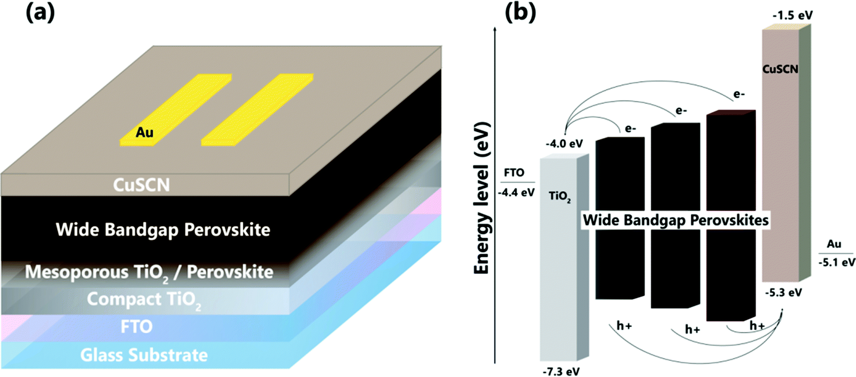 | ||
| Fig. 1 Architecture (a) and energy band diagram (b) of the wide-bandgap (WBG) perovskite solar cells (PSCs) fabricated in this work, with a superstrate (n–i–p) layer structure, under ambient environment with high humidity conditions (>70%). | ||
2. Results and discussion
2.1 Analysis of wide-bandgap (WBG) perovskite layers
WBG perovskite films of the type Cs0.17FA0.83PbI3−xBrx were first deposited on FTO-coated glass substrates for optical, structural and morphological characterization. The thicknesses of the layers measured by profilometry are approximately 550 ± 50 nm. It was observed that the change in Br content influences the layers’ morphology, causing surfaces wrinkles with roughness up to 45 nm as presented further below, but it does not have a considerable impact on the average thickness of the perovskite layers.Fig. 2a shows that the absorbance of the perovskite layers on the FTO substrates is more than 80% for the visible region and, depending on the bandgap value (determined by Br content, x), the absorbance onset changes in the near-infrared wavelength range. The energy bandgap (EG) values displayed in Fig. 2c were determined via the steady-state photoluminescence (PL) peaks (see Fig. 2b) and the Tauc plot method (see inset of Fig. 2a) for direct bandgap semiconductors. It can be clearly seen that the EG values increase linearly with higher Br content ratio, as expected. The slope of the linear regression displaying this characteristic is dEG/dx = 0.2–0.23 eV, which proves a facile tuning of the perovskite layer bandgap. The EG values obtained from absorbance and PL concur well, with slight differences that reduce as the Br content increases. Besides, the observed stronger PL intensities with increasing Br content (see Fig. S1 in ESI†) is in agreement with the crystallinity measurements described below.48
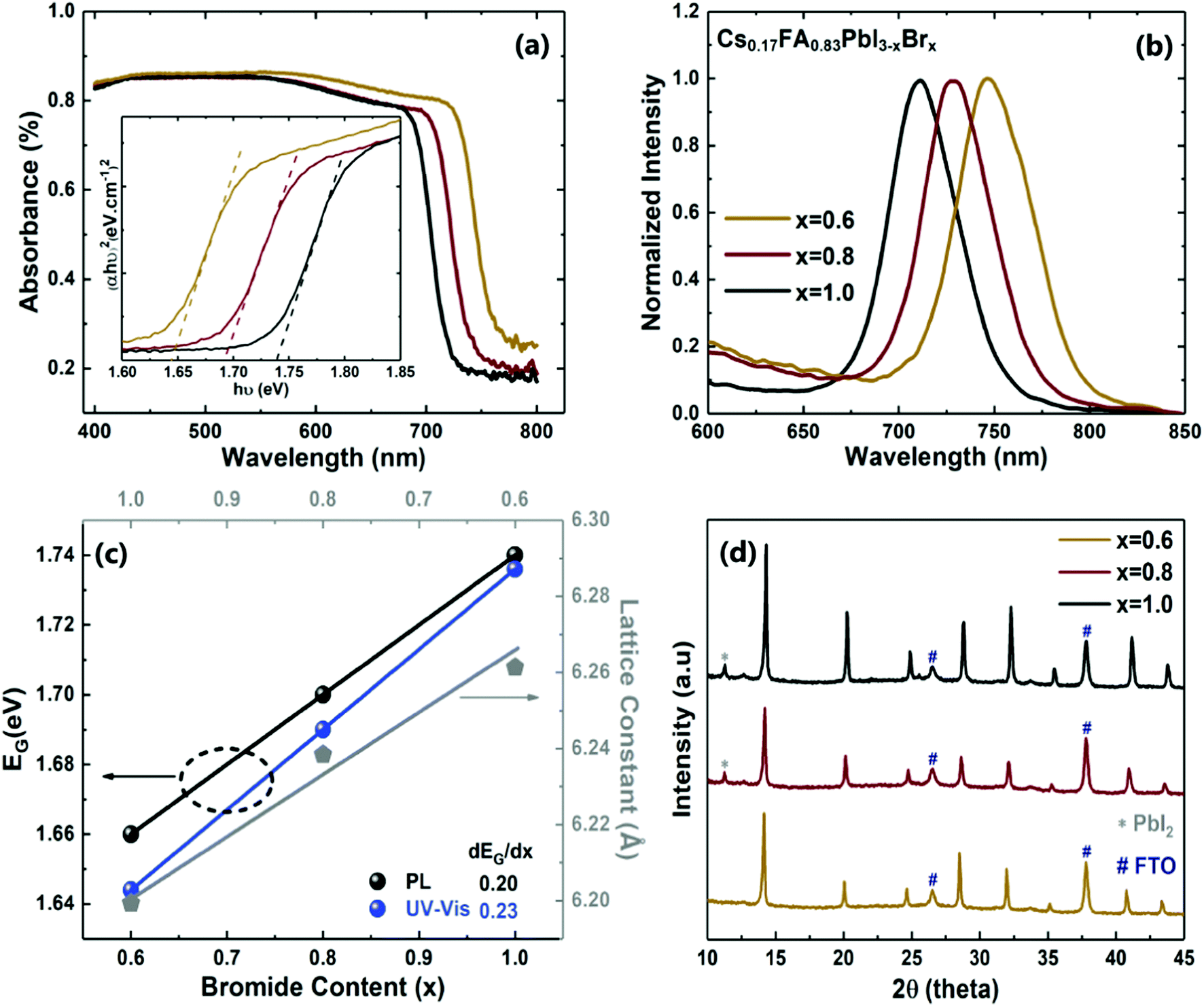 | ||
| Fig. 2 Optical and structural results of Cs0.17FA0.83PbI3−xBrx perovskite layers on FTO-coated glass substrates, with different Br content (x = 0.6, 0.8, 1.0). (a) Absorbance spectra with Tauc plots [(αhν)2vs. hν] in inset. (b) Normalized steady-state PL measurements. (c) Relation between the perovskite bandgap, EG, and the lattice constant, as a function of Br content. (d) X-Ray diffraction plots of the WBG perovskite layers, whose peaks are shown in further detail in Fig. S2 of the ESI.† | ||
The crystallinity of the perovskite layer is a key factor for the PSCs’ efficiency. To scrutinize the crystalline properties of the perovskite absorbers depending on Br content, we calculated the Urbach energies (EU) of the perovskite layers from the absorption spectra viaeqn (1):
| α = α0 + ehν/EU | (1) |
| x (Br content ratio) | 0.6 | 0.8 | 1.0 |
|---|---|---|---|
| Urbach energy (EU, meV) | 63 | 57 | 53 |
| RMS roughness (nm) | 29.68 | 42.29 | 45.02 |
| Mean grain size (nm) | 137.3 | 190.1 | 205.6 |
The aforementioned impact of Br content in the perovskite crystallization is confirmed by X-ray diffractometry (XRD) measurements shown in Fig. 2d. All samples display the perovskite peak around 2θ = 14.2°, referring to the (100) perovskite plane. Additionally, the peaks at 20°, 24.8°, 28° and 41.5° are also found in wide-bandgap perovskite layers.50 In general, with the increase of Br content the XRD peak intensities increase, indicating improved crystallinity. On the other hand, the perovskite layer with the lowest Br content (x = 0.6) does not exhibit any photoinactive PbI2 peaks (∼12.6°), which can be attributed to the lower precursor concentration, and thus better dissolubility and homogeneity of the perovskite solution. This sample also has a pronouncedly lower surface roughness determined from AFM measurements, as presented in Table 1 and discussed further below.
The XRD results show that, when increasing the Br![[thin space (1/6-em)]](https://www.rsc.org/images/entities/char_2009.gif) :I ratio, a slight shift to higher angle values occurs, as presented in further detail in Fig. S2 of ESI.† It is known that higher Br content causes the lattice to shrink, due to the smaller size of the bromide ion when compared with the iodide ion,17,51 which transforms the tetragonal phase of MAPbI3 into the cubic phase of pure MAPbBr3. The same behaviour occurs in FA and Cs mixed-cation perovskites.52 The lattice constant calculations (see Fig. 2c) for the main perovskite peak of 2θ = 14.2° confirm such lattice contraction, and the linear relation between the lattice constant and Br content matches Vegard's law.17
:I ratio, a slight shift to higher angle values occurs, as presented in further detail in Fig. S2 of ESI.† It is known that higher Br content causes the lattice to shrink, due to the smaller size of the bromide ion when compared with the iodide ion,17,51 which transforms the tetragonal phase of MAPbI3 into the cubic phase of pure MAPbBr3. The same behaviour occurs in FA and Cs mixed-cation perovskites.52 The lattice constant calculations (see Fig. 2c) for the main perovskite peak of 2θ = 14.2° confirm such lattice contraction, and the linear relation between the lattice constant and Br content matches Vegard's law.17
The AFM images (shown in Fig. S3, ESI†) indicate that when increasing x, the RMS surface roughness also increases (Table 1). The reduced roughness of the perovskites with lowest x should be caused by the homogeneity of the precursor solutions and Br:I ratio in the layers. Also, the change in the roughness with Br content is attributed to the wrinkled morphology of the layers, as visualized by scanning electron microscopy (SEM, see Fig. 3). As suggested in the literature, the wrinkled-shaped structures are a consequence of compact stress during the film formation, depending on the precursor solution, antisolvent washing and annealing step.53–55
 | ||
| Fig. 3 Low magnification SEM images of the WBG perovskite layers on FTO-coated glass substrates, composed with different Br content: (a) x = 0.6, (b) x = 0.8, (c) x = 1.0. It can be seen that the overall homogeneity is better for the perovskite with the lower Br content (and lower EG, displayed in top-right corner), while increased wrinkling is observed with higher x. | ||
Although the wrinkled surface morphology does not significantly affect the optical properties of the films, the device performance was reduced mainly due to the less conformal deposition of the hole transport layer.49,56 As shown in ESI† (Fig. S3), higher x leads to relatively deeper cracks in the films, which causes higher density of recombination centers, short-circuits and overall loss in the PSCs’ performance.57 Therefore, even though the perovskite layer with the highest Br content has better crystallinity properties and lower Urbach energy values, the resulting solar cell parameters were worse than the other cells, as shown in the next section.
Besides, as shown in the SEMs of Fig. 4 with higher magnification and in Table 1, with the increment of bromide content the average grain size of the perovskite films increases, mainly due to the appearance of large (>300 nm) grains causing a higher positive skewness (i.e. lower homogeneity) of the size distribution.
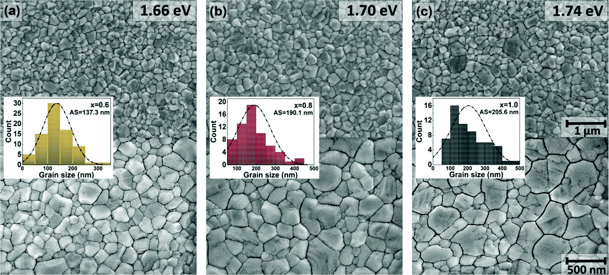 | ||
| Fig. 4 Top-view SEM images of the WBG perovskite layers on FTO-coated glass substrates, composed with different Br content: (a) x = 0.6, (b) x = 0.8, (c) x = 1.0. The images reveal the multi-crystalline grain structure of the films at two different magnifications. The inset histograms show the grain size distribution and average grain size (AS, also indicated in Table 1). | ||
2.2 PSCs’ optoelectronic assessment and optimization
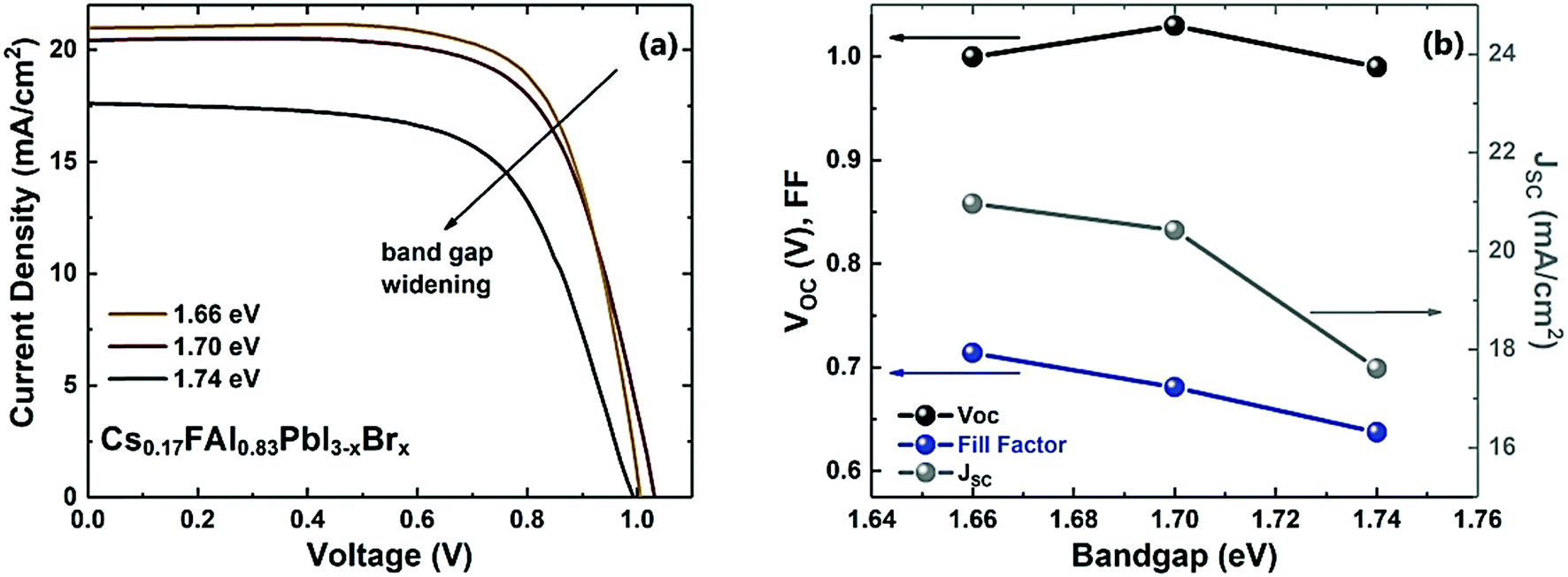 | ||
| Fig. 5 J–V curves (a) and variation of characteristic parameters (b) of the WBG PSCs with the EG values. | ||
| E g (eV) | V oc (V) | J sc (mA cm−2) | FF | PCE (%) | R series (Ω) | R shunt (Ω) |
|---|---|---|---|---|---|---|
| 1.66 | 1.00 | 20.96 | 0.71 | 15.1 | 62.8 | 25517 |
| 1.70 | 1.03 | 20.43 | 0.68 | 14.4 | 86.6 | 32335 |
| 1.74 | 0.99 | 17.61 | 0.64 | 11.1 | 120 | 13734 |
As expected, there is a reduction in the PCE with increasing EG of the perovskite absorber. However, an opposite trend should have been observed for the open-circuit voltage (Voc), but here that is not the case since the Voc deficit  increases with the bandgap widening (see Fig. S4, ESI†). This effect is attributed to inevitable phase segregation in the perovskite layer, which becomes more pronounced when the fabrication occurs in a humid environment.58,59 Also, the aforementioned non-ideal interface properties, between the perovskite and charge transport layers, cause Voc reduction and higher series resistance. As for the shunt resistance (Rshunt), it does not present a linear trend since it is higher for the mid-bandgap solar cell relative to the others.
Regarding the short-circuit current density (JSC), it decreases with higher bandgap of the perovskite layer. This is expected optically since the absorbance onset is blue-shifted, as seen in Fig. 2a.60 In addition, the increased roughness with higher Br content causes more charge recombination at the interfaces, which also justifies the decrease of the fill factor (FF) values.61
Although the highest PCE of this set was attained with the 1.66 eV bandgap perovskite, the higher Voc and Rshunt with the 1.70 eV perovskite motivated a subsequent study focused in the improvement of the 1.70 eV PSCs, in view of their promising application for tandem solar cells due to the suitable bandgap value.
| Best results: | E g (eV) | V oc (V) | J sc (mA cm−2) | FF | PCE (%) | R series (Ω) | R shunt (Ω) |
|---|---|---|---|---|---|---|---|
| 1.70 | 1.08 | 21.0 | 0.72 | 16.4 | 73.2 | 25244 |
In Fig. 6, the cross-sectional SEM shows that the perovskite layer thickness is in the 560–600 nm range, exhibiting some defects in the layer bulk and at both interfaces with the ETL and HTL. This reveals that there is still room for improvement in order to further increase the performance, and reach that of state-of-the-art cells produced in a controlled glovebox environment. Moreover, the dark I–V characteristic (Fig. S5, ESI†) shows a high leakage current in reverse bias, causing a worse diode character, and thus reduced efficiency, compared to the record literature values with similar WBG–PSC structures. This also contributes to the commonly observed hysteresis effect of PSCs, shown in Fig. S6 of ESI,† attributed to the mobile ions/ion-vacancies in the perovskite material which cause a pronounced dependence of the cell JV characteristic with the scan direction.
 | ||
| Fig. 6 Cross-sectional SEM-FIB image of FTO/TiO2/(CsI)0.17(FAI)0.83(PbI2)0.6(PbBr2)0.4/CuSCN/Au solar cell. | ||
As referred before, Wang et al.31 described a “turbid point (TP)” observed during the perovskite layer deposition when the transparent perovskite film becomes turbid during the spin coating, and this point is dependent on the humidity levels of the ambient air. In our work, the most efficient PSC was achieved by preheating the substrates and applying antisolvent (chlorobenzene, CB) dripping 1–2 seconds before the turbid point, as well as by using warm antisolvent to help the solvent evaporation process and removal of oxygen and water. When the perovskite layers were deposited in ≤50% RH, compatible with Wang's observations, the turbid point appears sooner, and as a result, a thinner layer grows. We also applied the CB washing placing the pipette tip very close (less than 5 mm) to the substrate, and noticed a significant enhancement on the perovskite layer formation. This impact can be attributed to speeding up the evaporation process, hence promoting better layer crystallization. Fig. S7 in ESI† shows the effects of key fabrication steps in the resulting JV curves of the PSCs, whose optimization essentially allows minimizing the defect density in the perovskite layer and, thereby, improving the devices’ performance. All in all, this study reinforces Wang's humidity insensitive antisolvent method, providing further understanding of the process of PSCs fabrication in humid ambient air.
To confirm the PSCs reproducibility, we fabricated more than 100 solar cells with WBG perovskite layers in the FTO/compact-TiO2/meso-TiO2/(CsI)0.17(FAI)0.83(PbI2)0.6(PbBr2)0.4/CuSCN/Au configuration, and under ∼70% RH ambient conditions. The J–V characteristics and external quantum efficiency (EQE) measurements of the best performing cell are shown in Fig. 7a and b. The integrated current density values derived from the EQE spectra match that of the J–V characteristics acquired with the solar simulator. Remarkably, without any encapsulation the best performing solar cell kept more than 80% of its initial efficiency for more than 3500 hours, and almost 70% after 4500 hours, which is shown in Fig. 7c.
In Fig. 7d, the solar cell parameters of the EG = 1.7 eV PSCs are displayed over 100 fabricated devices. The main noteworthy aspect is that, although the humidity and temperature conditions in the laboratory are not controlled, the optimized process developed in this work allows highly reproducible cells with high efficiency values. The average of the Voc, Jsc, FF and PCE values are 1.05 V, 19.9 mA cm−2, 0.70 and 14.4%, respectively. These results are among the best attained up to now in the PSCs’ field, namely in comparison with the previous reported advances attained with un-encapsulated WBG PSCs fabricated in ambient humidity conditions.62,63
 | ||
| Fig. 7 J–V characteristic under AM 1.5 illumination (a), and EQE spectrum (b) of the best performing WBG (1.70 eV) PSC, which presents remarkable stability up to 4500 hours (c) even without any cell encapsulation. (d) Distribution and statistical analysis of the solar cell parameters of over 100 fabricated cells. | ||
3. Conclusions
We present a low-cost glovebox-free procedure to contrive WBG PSCs, whose optical bandgap values were tuned between 1.66 to 1.74 eV by changing the Br content in the perovskite structure. Here, the wrinkled morphology of the surface deteriorated the interface properties, and thus caused relatively lower efficiency for higher Br:I ratio. The perovskite layer with 1.70 eV bandgap was selected for further optimization due to its potential application in tandem devices. A large set of mixed-cation mixed-halide WBG PSCs with FTO/compact-TiO2/meso-TiO2/(CsI)0.17(FAI)0.83(PbI2)0.6(PbBr2)0.4/CuSCN/Au configuration were fabricated, in which a record cell is reported with the best efficiency (16.4%) attained thus far for ambient-processed WBG PSCs. In addition, this cell presents a remarkable stability, maintaining 80% of the initial efficiency for 3500 hours, and 70% up to 4500 hours. These outcomes reveal that it is possible to reproducibly fabricate high-performing and stable WBG PSCs without a controlled glovebox environment, and employing inexpensive charge transport materials such as the one used here (CuSCN) which is much cheaper than the conventional organic-based HTLs. This was attained via a humidity-insensitive antisolvent method, in which it was found crucial to preheat the substrate before the perovskite deposition, as well as to preheat the antisolvent and apply the antisolvent washing from a very close tip-sample distance, which enhances the evaporation and crystallization process of the perovskite film by reducing the moisture effects.In addition to the set of morphological, structural and optoelectronic characterization techniques employed in this work, further insight into the role of the resulting bulk and interfaces’ properties on the PSCs’ transport mechanisms can be gained via electrochemical impedance/admittance analysis, which can also probe and provide a better understanding of the charge distribution and transfer within the PSC structure, including ion migration and, thus, hysteresis effects, as discussed in related works.38,64–68
Lastly, the main avenues that should be explored for further advances are the extended optimization of the absorber layer with wider (up to ∼2 eV) bandgap values, in view of application in tandem devices with silicon and low bandgap PSCs. Additionally, the implementation of photonic structures in the PSCs should be pursued, not only as a means to increase the photocurrent generation (and thereby the PCE) via light capturing and trapping,69 but also to improve the devices’ stability against UV70,71 and water72 penetration as demonstrated in recent contributions.
Experimental methods
Materials
All chemical reagents used in this study were purchased from commercial vendors. Formamidinium iodide (FAI) (Sigma Aldrich), lead iodide (PbI2) (Sigma Aldrich), ceasium iodide (CsI) (Acros Organics), lead bromide (PbBr2) (Sigma Aldrich), titanium IV-isopropoxide (TTIP) (Sigma Aldrich), titanium dioxide (TiO2) paste (Sigma Aldrich), copper(I) thiocyanate (CuSCN) (Alfa Aeasar), diethyl sulfide (DES) (Sigma Aldrich), dimethylformamide (DMF) (Fisher Chemical), dimethyl sulfoxide (DMSO) (Panreac), chlorobenzene (CB) (Alfa Aeasar) were used without further purification.Substrate preparation and ETL layer deposition
The wide-bandgap perovskite solar cells were fabricated with mesoscopic structure: Glass/FTO/TiO2/Cs0.17FA0.83PbI3−xBrx/CuSCN/Au. All the preparations and layer depositions were performed in ambient air with RH > 70%.FTO-coated glasses (13 Ω sq−1, 82–84.5% of transmittance) were cut into 2 × 2 cm, then a 2 mm stripe of the FTO layer was etched with zinc powder and HCl solution, and afterwards cleaned by sonication with Hellmanex II, water, acetone, isopropanol alcohol and an additional step of UV-O3 treatment to remove the organic compounds right before the deposition of the electron transport layer (ETL).
The first deposited layer of the solar cell is a very thin compact TiO2 film. The solution is prepared by a two-step method. Firstly, 180 μl of TTIP was added to 1.25 ml of absolute ethanol and placed onto a stirrer, and then 1.25 ml of absolute ethanol with 18 μl of HCL was added to the main solution. The compact TiO2 layers were deposited by spin coating for 35 seconds at 4000 rpm. After the spin coating, the layers were dried at 100 °C for 10 minutes, and then sintered in a furnace at 500 °C in ambient air. After the samples cool down to room temperature, another UV-O3 treatment was applied for 15 minutes before the mesoporous TiO2 layer deposition. For this layer, 120 mg of titania paste was dissolved in 1 ml absolute ethanol and deposited by spin coating for 20 seconds at 4000 rpm, followed by a drying step at 120 °C for 10 minutes and sintering at 450 °C for 30 minutes in ambient air.
Perovskite solutions and deposition
The perovskite precursor solutions were prepared with the composition of (CsI)0.17(FAI)0.83(PbI2)1−0.5x(PbBr2)0.5x using different bromide content by dissolving CsI (88.9 mg), FAI (285 mg) and PbI2, PbBr2 in 1 ml mixture of DMF and DMSO (with a volume ratio of 9:1). For the bandgap variation, x was chosen as 0.6, 0.8 and 1 during the precursor solution preparation. The precursor solutions were stirred at 70 °C until they reach a bright yellow colour. The solutions were filtered by a PTFE filter and the substrates coated with the ETL were heated up to 70 °C right before the deposition. The perovskite layer was deposited via a single-step deposition method with two different spin rates: 1000 rpm for 10 seconds and then increases to followed by an increase to 5000 rpm for a 20 seconds spin. Chlorobenzene was poured during the spinning at the higher spin rate to remove the solvents of the perovskite solution and improve crystallization. Soon after the deposition of the perovskite layer, the samples are annealed at 110 °C for 20 minutes on a hot plate covered by a Petri dish. As soon as the annealing process starts the layers turn to dark brown color from a light yellow one.
Hole transport layer and metal contact deposition
Following the perovskite layer deposition, CuSCN (copper(I) thiocyanate) was used as the hole transport material. Dissolving in diethyl sulfide, the solution was prepared as 0.3 M, filtered by a 0.45 μm filter and deposited by spin coating for 20 s at 4000 rpm, followed by 5 minute annealing applied at 90 °C to evaporate the HTL solvent to avoid the deterioration of the perovskite layer. The gold back contacts were deposited by e-beam evaporation under high vacuum at a low deposition rate. The cells were produced with an active area of 0.10 cm2.Characterization techniques
The optical transmission measurements were performed by UV-Vis-NIR spectrophotometry (PerkinElmer Lambda 950) in 300–800 nm wavelength range. Steady-state photoluminescence (PL) was measured by a PerkinElmer LS55, with an excitation at 400 nm. Scanning Electron Microscopy (SEM) surface images were acquired by a TM3030 Plus Hitachi for lower and a Hitachi Regulus 8220 for higher magnification observations, and the corresponding grain size analysis was performed via ImageJ software. For the cross-sectional imaging, a Carl Zeiss AURIGA Cross Beam SEM work station was used. Surface topography Atomic Force Microscopy (AFM) images were obtained by an Asylum Research MFP-3D Standalone system using commercially available silicon AFM probes (Olympus AC160TS, f0 = 300 kHz, k = 26 N m−1). The X-ray diffraction (XRD) patterns were collected on a PANalytical XPert Pro X-ray powder diffractometer using Cu-Ka radiation (λ = 1.54050 Å). The J–V measurements were performed with Newport's Oriel® VeraSol LSH-7520 LED-based Solar Simulator (100 mW cm−2) under AM 1.5 conditions, calibrated by a crystalline silicon reference cell (from VLSI Standards Inc.), in ambient conditions. A Keithley 2500 power source was used to apply voltages and collect current from the devices. The Quantum Efficiency measurements of the solar cells were carried out by Newport's QUANTX-300 system.Conflicts of interest
There are no conflicts to declare.Acknowledgements
This work was funded by FCT (Fundação para a Ciência e Tecnologia, I.P.) under the projects UIDB/50025/2020, SuperSolar (PTDC/NAN-OPT/28430/2017) and TACIT (PTDC/NAN-OPT/28837/2017). We also acknowledge the support of SYNERGY, H2020-WIDESPREAD-2020-5, CSA, proposal n° 952169. U. D. Menda and G. Ribeiro acknowledge funding from FCT through the grants UIDP/50025/2020 and SFRH/BD/151095/2021, respectively.References
- A. Kojima, K. Teshima, Y. Shirai and T. Miyasaka, Organometal halide perovskites as visible-light sensitizers for photovoltaic cells, J. Am. Chem. Soc., 2009, 131, 6050–6051, DOI:10.1021/ja809598r.
- NREL Best Research-Cell Efficiency Chart, (n.d.). https://www.nrel.gov/pv/cell-efficiency.html (accessed February 1, 2021).
- M. J. Brites, M. A. Barreiros, V. Corregidor, L. C. Alves, J. V. Pinto, M. J. Mendes, E. Fortunato, R. Martins and J. Mascarenhas, Ultrafast Low-Temperature Crystallization of Solar Cell Graded Formamidinium-Cesium Mixed-Cation Lead Mixed-Halide Perovskites Using a Reproducible Microwave-Based Process, ACS Appl. Energy Mater., 2019, 2, 1844–1853, DOI:10.1021/acsaem.8b02005.
- J. Troughton, D. Bryant, K. Wojciechowski, M. J. Carnie, H. Snaith, D. A. Worsley and T. M. Watson, Highly efficient, flexible, indium-free perovskite solar cells employing metallic substrates, J. Mater. Chem. A, 2015, 3, 9141–9145, 10.1039/c5ta01755f.
- F. Yang, J. Liu, H. E. Lim, Y. Ishikura, K. Shinokita, Y. Miyauchi, A. Wakamiya, Y. Murata and K. Matsuda, High Bending Durability of Efficient Flexible Perovskite Solar Cells Using Metal Oxide Electron Transport Layer, J. Phys. Chem. C, 2018, 122, 17088–17095, DOI:10.1021/acs.jpcc.8b05008.
- P. Docampo, J. M. Ball, M. Darwich, G. E. Eperon and H. J. Snaith, Efficient organometal trihalide perovskite planar-heterojunction solar cells on flexible polymer substrates, Nat. Commun., 2013, 4, 1–6, DOI:10.1038/ncomms3761.
- F. Fu, T. P. Weiss, F. Fu, T. Feurer, T. P. Weiss, S. Pisoni, E. Avancini, C. Andres, S. Buecheler and A. N. Tiwari, High-efficiency inverted semi-transparent planar perovskite solar cells in substrate configuration, Nat. Energy, 2016, 1, 1690, DOI:10.1038/nenergy.2016.190.
- J. Werner, C. C. Boyd, T. Moot, E. J. Wolf, R. M. France, S. A. Johnson, M. F. A. M. van Hest, J. M. Luther, K. Zhu, J. J. Berry and M. D. McGehee, Learning from existing photovoltaic technologies to identify alternative perovskite module designs, Energy Environ. Sci., 2020, 13, 3393–3403, 10.1039/d0ee01923b.
- Y. Zhou, F. Wang, H. H. Fang, M. A. Loi, F. Y. Xie, N. Zhao and C. P. Wong, Distribution of bromine in mixed iodide-bromide organolead perovskites and its impact on photovoltaic performance, J. Mater. Chem. A, 2016, 4, 16191–16197, 10.1039/c6ta07647e.
- J. H. Heo, D. H. Song and S. H. Im, Planar CH3NH3PbBr3 hybrid solar cells with 10.4% power conversion efficiency, fabricated by controlled crystallization in the spin-coating process, Adv. Mater., 2014, 26, 8179–8183, DOI:10.1002/adma.201403140.
- G. E. Eperon, T. Leijtens, K. A. Bush, R. Prasanna, T. Green, J. T. W. Wang, D. P. McMeekin, G. Volonakis, R. L. Milot, R. May, A. Palmstrom, D. J. Slotcavage, R. A. Belisle, J. B. Patel, E. S. Parrott, R. J. Sutton, W. Ma, F. Moghadam, B. Conings, A. Babayigit, H. G. Boyen, S. Bent, F. Giustino, L. M. Herz, M. B. Johnston, M. D. McGehee and H. J. Snaith, Perovskite-perovskite tandem photovoltaics with optimized band gaps, Science, 2016, 354, 861–865, DOI:10.1126/science.aaf9717.
- J. H. Heo and S. H. Im, CH3NH3PbBr3–CH3NH3PbI3Perovskite–Perovskite Tandem Solar Cells with Exceeding 2.2 V Open Circuit Voltage, Adv. Mater., 2016, 5121–5125, DOI:10.1002/adma.201501629.
- D. Forgács, D. Pérez-Del-Rey, J. Ávila, C. Momblona, L. Gil-Escrig, B. Dänekamp, M. Sessolo and H. J. Bolink, Efficient wide band gap double cation-double halide perovskite solar cells, J. Mater. Chem. A, 2017, 5, 3203–3207, 10.1039/c6ta10727c.
- C. G. Wu, C. H. Chiang and S. H. Chang, A perovskite cell with a record-high-Voc of 1.61 v based on solvent annealed CH3NH3PbBr3/ICBA active layer, Nanoscale, 2016, 8, 4077–4085, 10.1039/c5nr07739g.
- K. A. Bush, A. F. Palmstrom, Z. J. Yu, M. Boccard, R. Cheacharoen, J. P. Mailoa, D. P. McMeekin, R. L. Z. Hoye, C. D. Bailie, T. Leijtens, I. M. Peters, M. C. Minichetti, N. Rolston, R. Prasanna, S. Sofia, D. Harwood, W. Ma, F. Moghadam, H. J. Snaith, T. Buonassisi, Z. C. Holman, S. F. Bent and M. D. McGehee, 23.6%-Efficient Monolithic Perovskite/Silicon Tandem Solar Cells With Improved Stability, Nat. Energy, 2017, 2, 17009, DOI:10.1038/nenergy.2017.9.
- M. Chapa, M. F. Alexandre, M. J. Mendes, H. Águas, E. Fortunato and R. Martins, All-Thin-Film Perovskite/C-Si Four-Terminal Tandems: Interlayer and Intermediate Contacts Optimization, ACS Appl. Energy Mater., 2019, 2, 3979–3985, DOI:10.1021/acsaem.9b00354.
- D. P. McMeekin, G. Sadoughi, W. Rehman, G. E. Eperon, M. Saliba, M. T. Hörantner, A. Haghighirad, N. Sakai, L. Korte, B. Rech, M. B. Johnston, L. M. Herz and H. J. Snaith, A mixed-cation lead mixed-halide perovskite absorber for tandem solar cells, Science, 2016, 351, 151–155, DOI:10.1126/science.aad5845.
- T. J. Jacobsson, A. Hultqvist, S. Svanström, L. Riekehr, U. B. Cappel, E. Unger, H. Rensmo, E. M. J. Johansson, M. Edoff and G. Boschloo, 2-Terminal CIGS-perovskite tandem cells: A layer by layer exploration, Sol. Energy, 2020, 207, 270–288, DOI:10.1016/j.solener.2020.06.034.
- H. Shen, T. Duong, J. Peng, D. Jacobs, N. Wu, J. Gong, Y. Wu, S. K. Karuturi, X. Fu, K. Weber, X. Xiao, T. P. White and K. Catchpole, Mechanically-stacked perovskite/CIGS tandem solar cells with efficiency of 23.9% and reduced oxygen sensitivity, Energy Environ. Sci., 2018, 11, 394–406, 10.1039/c7ee02627g.
- Z. Song, C. L. McElvany, A. B. Phillips, I. Celik, P. W. Krantz, S. C. Watthage, G. K. Liyanage, D. Apul and M. J. Heben, A technoeconomic analysis of perovskite solar module manufacturing with low-cost materials and techniques, Energy Environ. Sci., 2017, 10, 1297–1305, 10.1039/c7ee00757d.
- N. L. Chang, A. W. Yi Ho-Baillie, P. A. Basore, T. L. Young, R. Evans and R. J. Egan, A manufacturing cost estimation method with uncertainty analysis and its application to perovskite on glass photovoltaic modules, Prog. Photovoltaics Res. Appl., 2017, 25, 390–405, DOI:10.1002/pip.2871.
- F. Sahli, J. Werner, B. A. Kamino, M. Bräuninger, R. Monnard, B. Paviet-Salomon, L. Barraud, L. Ding, J. J. Diaz Leon, D. Sacchetto, G. Cattaneo, M. Despeisse, M. Boccard, S. Nicolay, Q. Jeangros, B. Niesen and C. Ballif, Fully textured monolithic perovskite/silicon tandem solar cells with 25.2% power conversion efficiency, Nat. Mater., 2018, 17, 820–826, DOI:10.1038/s41563-018-0115-4.
- M. Saliba, J. P. Correa-Baena, C. M. Wolff, M. Stolterfoht, N. Phung, S. Albrecht, D. Neher and A. Abate, How to Make over 20% Efficient Perovskite Solar Cells in Regular (n–i–p) and Inverted (p–i–n) Architectures, Chem. Mater., 2018, 30, 4193–4201, DOI:10.1021/acs.chemmater.8b00136.
- N. Yaghoobi Nia, M. Zendehdel, L. Cinà, F. Matteocci and A. Di Carlo, A crystal engineering approach for scalable perovskite solar cells and module fabrication: A full out of glove box procedure, J. Mater. Chem. A, 2018, 6, 659–671, 10.1039/c7ta08038g.
- J. Yin, J. Cao, X. He, S. Yuan, S. Sun, J. Li, N. Zheng and L. Lin, Improved stability of perovskite solar cells in ambient air by controlling the mesoporous layer, J. Mater. Chem. A, 2015, 3, 16860–16866, 10.1039/c5ta02843d.
- W. H. Chen, L. Qiu, Z. Zhuang, L. Song, P. Du, J. Xiong and F. Ko, Simple fabrication of perovskite solar cells with enhanced efficiency, stability, and flexibility under ambient air, J. Power Sources, 2019, 442, 1–8, DOI:10.1016/j.jpowsour.2019.227216.
- F. Wang, Y. Zhongbiao, H. Sarvari, S. Park, K. Graham, Y. Zhao and Z. David Chen, Fabrication of Efficient CH3NH3PbI3 Solar Cells in Ambient Air, 2017 IEEE 44th Photovoltaic Specialist Conference (PVSC), 2018, 1044–1047, DOI:10.1109/pvsc.2017.8520927.
- F. P. Gokdemir Choi, H. Moeini Alishah, S. Bozar, C. Doyranli, S. Koyuncu, N. San, C. Kahveci, M. Cantürk Rodop, M. B. Arvas, M. Gencten, Y. Sahin and S. Gunes, A novel interface layer for inverted perovskite solar cells fabricated in ambient air under high humidity conditions, Sol. Energy, 2020, 209, 400–407, DOI:10.1016/j.solener.2020.08.013.
- S. Pathak, A. Sepe, A. Sadhanala, F. Deschler, A. Haghighirad, N. Sakai, K. C. Goedel, S. D. Stranks, N. Noel, M. Price, S. Hüttner, N. A. Hawkins, R. H. Friend, U. Steiner and H. J. Snaith, Atmospheric influence upon crystallization and electronic disorder and its impact on the photophysical properties of organic–inorganic perovskite solar cells, ACS Nano, 2015, 9, 2311–2320, DOI:10.1021/nn506465n.
- J. Troughton, K. Hooper and T. M. Watson, Humidity resistant fabrication of CH3NH3PbI3 perovskite solar cells and modules, Nano Energy, 2017, 39, 60–68, DOI:10.1016/j.nanoen.2017.06.039.
- F. Wang, T. Zhang, Y. Wang, D. Liu, P. Zhang, H. Chen, L. Ji, L. Chen, Z. D. Chen, J. Wu, X. Liu, Y. Li and S. Li, Steering the crystallization of perovskites for high-performance solar cells in ambient air, J. Mater. Chem. A, 2019, 7, 12166–12175, 10.1039/c9ta02566a.
- K. Sveinbjörnsson, K. Aitola, J. Zhang, M. B. Johansson, X. Zhang, J. P. Correa-Baena, A. Hagfeldt, G. Boschloo and E. M. J. Johansson, Ambient air-processed mixed-ion perovskites for high-efficiency solar cells, J. Mater. Chem. A, 2016, 4, 16536–16545, 10.1039/c6ta06912f.
- Y. Cheng, X. Xu, Y. Xie, H. W. Li, J. Qing, C. Ma, C. S. Lee, F. So and S. W. Tsang, 18% High-Efficiency Air-Processed Perovskite Solar Cells Made in a Humid Atmosphere of 70% RH, Sol. RRL, 2017, 1, 1–8, DOI:10.1002/solr.201700097.
- S. S. Shin, S. J. Lee and S. I. Seok, Exploring wide bandgap metal oxides for perovskite solar cells, APL Mater., 2019, 7, 022401, DOI:10.1063/1.5055607.
- N. Arora, M. I. Dar, A. Hinderhofer, N. Pellet, F. Schreiber, S. M. Zakeeruddin and M. Grätzel, Perovskite solar cells with CuSCN hole extraction layers yield stabilized efficiencies greater than 20%, Science, 2017, 358, 768–771, DOI:10.1126/science.aam5655.
- C. Yang, M. Yu, D. Chen, Y. Zhou, W. Wang, Y. Li, T. C. Lee and D. Yun, An annealing-free aqueous-processed anatase TiO2 compact layer for efficient planar heterojunction perovskite solar cells, Chem. Commun., 2017, 53, 10882–10885, 10.1039/c7cc01104k.
- M. Saliba, S. Orlandi, T. Matsui, S. Aghazada, M. Cavazzini, J. P. Correa-Baena, P. Gao, R. Scopelliti, E. Mosconi, K. H. Dahmen, F. De Angelis, A. Abate, A. Hagfeldt, G. Pozzi, M. Graetzel and M. K. Nazeeruddin, A molecularly engineered hole-transporting material for efficient perovskite solar cells, Nat. Energy, 2016, 1, 1–7, DOI:10.1038/nenergy.2015.17.
- H. H. Wang, Q. Chen, H. Zhou, L. Song, Z. St Louis, N. De Marco, Y. Fang, P. Sun, T. Bin Song, H. Chen and Y. Yang, Improving the TiO2 electron transport layer in perovskite solar cells using acetylacetonate-based additives, J. Mater. Chem. A, 2015, 3, 9108–9115, 10.1039/c4ta06394e.
- B. Wang, M. Zhang, X. Cui, Z. Wang, M. Rager, Y. Yang, Z. Zou, Z. L. Wang and Z. Lin, Unconventional Route to Oxygen-Vacancy-Enabled Highly Efficient Electron Extraction and Transport in Perovskite Solar Cells, Angew. Chem., Int. Ed., 2020, 59, 1611–1618, DOI:10.1002/anie.201910471.
- H. Li, Y. Xue, B. Zheng, J. Tian, H. Wang, C. Gao and X. Liu, Interface modification with PCBM intermediate layers for planar formamidinium perovskite solar cells, RSC Adv., 2017, 7, 30422–30427, 10.1039/c7ra04311b.
- C. Lu, I. T. Choi, J. Kim and H. K. Kim, Simple synthesis and molecular engineering of low-cost and star-shaped carbazole-based hole transporting materials for highly efficient perovskite solar cells, J. Mater. Chem. A, 2017, 5, 20263–20276, 10.1039/c7ta04762b.
- T. P. I. Saragi, T. Spehr, A. Siebert, T. Fuhrmann-Lieker and J. Salbeck, Spiro compounds for organic optoelectronics, Chem. Rev., 2007, 107, 1011–1065, DOI:10.1021/cr0501341.
- A. T. Murray, J. M. Frost, C. H. Hendon, C. D. Molloy, D. R. Carbery and A. Walsh, Modular design of SPIRO-OMeTAD analogues as hole transport materials in solar cells, Chem. Commun., 2015, 51, 8935–8938, 10.1039/c5cc02129d.
- I. S. Yang, S. Lee, J. Choi, M. T. Jung, J. Kim and W. I. Lee, Enhancement of open circuit voltage for CuSCN-based perovskite solar cells by controlling the perovskite/CuSCN interface with functional molecules, J. Mater. Chem. A, 2019, 7, 6028–6037, 10.1039/c8ta12217b.
- F. Ma, Y. Zhao, J. Li, X. Zhang, H. Gu and J. You, Nickel oxide for inverted structure perovskite solar cells, J. Energy Chem., 2020, 52, 393–411, DOI:10.1016/j.jechem.2020.04.027.
- T. Abzieher, S. Moghadamzadeh, F. Schackmar, H. Eggers, F. Sutterlüti, A. Farooq, D. Kojda, K. Habicht, R. Schmager, A. Mertens, R. Azmi, L. Klohr, J. A. Schwenzer, M. Hetterich, U. Lemmer, B. S. Richards, M. Powalla and U. W. Paetzold, Electron-Beam-Evaporated Nickel Oxide Hole Transport Layers for Perovskite-Based Photovoltaics, Adv. Energy Mater., 2019, 9, 1–13, DOI:10.1002/aenm.201802995.
- P. Yang, J. Wang, X. Zhao, J. Wang, Z. Hu, Q. Huang and L. Yang, Magnetron-sputtered nickel oxide films as hole transport layer for planar heterojunction perovskite solar cells, Appl. Phys. A: Mater. Sci. Process., 2019, 125, 1–6, DOI:10.1007/s00339-019-2769-4.
- R. Segovia, G. Qu, M. Peng, X. Sun, H. Shi and B. Gao, Evolution of Photoluminescence, Raman, and Structure of CH3NH3PbI3 Perovskite Microwires Under Humidity Exposure, Nanoscale Res. Lett., 2018, 13, 0–7, DOI:10.1186/s11671-018-2470-0.
- A. Tejada, S. Braunger, L. Korte, S. Albrecht, B. Rech and J. A. Guerra, Optical characterization and bandgap engineering of flat and wrinkle-textured FA0.83Cs0.17Pb(I1−xBrx)3 perovskite thin films, J. Appl. Phys., 2018, 123, 0–7, DOI:10.1063/1.5025728.
- M. Saliba, T. Matsui, J. Y. Seo, K. Domanski, J. P. Correa-Baena, M. K. Nazeeruddin, S. M. Zakeeruddin, W. Tress, A. Abate, A. Hagfeldt and M. Grätzel, Cesium-containing triple cation perovskite solar cells: Improved stability, reproducibility and high efficiency, Energy Environ. Sci., 2016, 9, 1989–1997, 10.1039/c5ee03874j.
- R. Garc, D. Ferdani, S. Pering and P. J. Baker, Influence of bromide content on iodide migration in inverted MAPb(I1−xBrx)3 perovskite solar cells, J. Mater. Chem. A, 2019, 22604–22614, 10.1039/c9ta08848b.
- W. Rehman, D. P. McMeekin, J. B. Patel, R. L. Milot, M. B. Johnston, H. J. Snaith and L. M. Herz, Photovoltaic mixed-cation lead mixed-halide perovskites: Links between crystallinity, photo-stability and electronic properties, Energy Environ. Sci., 2017, 10, 361–369, 10.1039/c6ee03014a.
- K. A. Bush, N. Rolston, A. Gold-Parker, S. Manzoor, J. Hausele, Z. J. Yu, J. A. Raiford, R. Cheacharoen, Z. C. Holman, M. F. Toney, R. H. Dauskardt and M. D. McGehee, Controlling Thin-Film Stress and Wrinkling during Perovskite Film Formation, ACS Energy Lett., 2018, 3, 1225–1232, DOI:10.1021/acsenergylett.8b00544.
- S. Braunger, L. E. Mundt, C. M. Wolff, M. Mews, C. Rehermann, M. Jošt, A. Tejada, D. Eisenhauer, C. Becker, J. A. Guerra, E. Unger, L. Korte, D. Neher, M. C. Schubert, B. Rech and S. Albrecht, CsxFA1−xPb(I1−yBry)3 Perovskite Compositions: The Appearance of Wrinkled Morphology and its Impact on Solar Cell Performance, J. Phys. Chem. C, 2018, 122, 17123–17135, DOI:10.1021/acs.jpcc.8b06459.
- B. Chen, S. W. Baek, Y. Hou, E. Aydin, M. De Bastiani, B. Scheffel, A. Proppe, Z. Huang, M. Wei, Y. K. Wang, E. H. Jung, T. G. Allen, E. Van Kerschaver, F. P. García de Arquer, M. I. Saidaminov, S. Hoogland, S. De Wolf and E. H. Sargent, Enhanced optical path and electron diffusion length enable high-efficiency perovskite tandems, Nat. Commun., 2020, 11, 1257, DOI:10.1038/s41467-020-15077-3.
- R. E. Beal, N. Z. Hagström, J. Barrier, A. Gold-Parker, R. Prasanna, K. A. Bush, D. Passarello, L. T. Schelhas, K. Brüning, C. J. Tassone, H. G. Steinrück, M. D. McGehee, M. F. Toney and A. F. Nogueira, Structural Origins of Light-Induced Phase Segregation in Organic-Inorganic Halide Perovskite Photovoltaic Materials, Matter, 2020, 2, 207–219, DOI:10.1016/j.matt.2019.11.001.
- J. Ye, G. Liu, L. Jiang, H. Zheng, L. Zhu, X. Zhang, H. Wang, X. Pan and S. Dai, Crack-free perovskite layers for high performance and reproducible devices via improved control of ambient conditions during fabrication, Appl. Surf. Sci., 2017, 407, 427–433, DOI:10.1016/j.apsusc.2017.02.135.
- D. B. Khadka, Y. Shirai, M. Yanagida, T. Masuda and K. Miyano, Enhancement in efficiency and optoelectronic quality of perovskite thin films annealed in MACl vapor, Sustain, Energy Fuels, 2017, 1, 755–766, 10.1039/c7se00033b.
- S. Mahesh, J. M. Ball, R. D. J. Oliver, D. P. McMeekin, P. K. Nayak, M. B. Johnston and H. J. Snaith, Revealing the origin of voltage loss in mixed-halide perovskite solar cells, Energy Environ. Sci., 2020, 13, 258–267, 10.1039/c9ee02162k.
- M. I. Hossain, W. Qarony, S. Ma, L. Zeng, D. Knipp and Y. H. Tsang, Perovskite/Silicon Tandem Solar Cells: From Detailed Balance Limit Calculations to Photon Management, Nano-Micro Lett., 2019, 11, 58, DOI:10.1007/s40820-019-0287-8.
- K. T. Cho, S. Paek, G. Grancini, C. Roldán-Carmona, P. Gao, Y. Lee and M. K. Nazeeruddin, Highly efficient perovskite solar cells with a compositionally engineered perovskite/hole transporting material interface, Energy Environ. Sci., 2017, 10, 621–627, 10.1039/c6ee03182j.
- I. M. Asuo, D. Gedamu, N. Y. Doumon, I. Ka, A. Pignolet, S. G. Cloutier and R. Nechache, Ambient condition-processing strategy for improved air-stability and efficiency in mixed-cation perovskite solar cells, Mater. Adv., 2020, 1, 1866–1876, 10.1039/d0ma00528b.
- P. Luo, W. Xia, S. Zhou, L. Sun, J. Cheng, C. Xu and Y. Lu, Solvent Engineering for Ambient-Air-Processed, Phase-Stable CsPbI3 in Perovskite Solar Cells, J. Phys. Chem. Lett., 2016, 7, 3603–3608, DOI:10.1021/acs.jpclett.6b01576.
- L. Contreras-Bernal, S. Ramos-Terrón, A. Riquelme, P. P. Boix, J. Idígoras, I. Mora-Seró and J. A. Anta, Impedance analysis of perovskite solar cells: A case study, J. Mater. Chem. A, 2019, 7, 12191–12200, 10.1039/c9ta02808k.
- B. Hailegnaw, N. S. Sariciftci and M. C. Scharber, Impedance Spectroscopy of Perovskite Solar Cells: Studying the Dynamics of Charge Carriers Before and After Continuous Operation, Phys. Status Solidi A, 2020, 217, 1–8, DOI:10.1002/pssa.202000291.
- H. Wang, A. Guerrero, A. Bou, A. M. Al-Mayouf and J. Bisquert, Kinetic and material properties of interfaces governing slow response and long timescale phenomena in perovskite solar cells, Energy Environ. Sci., 2019, 12, 2054–2079, 10.1039/c9ee00802k.
- R. A. Awni, Z. Song, C. Chen, C. Li, C. Wang, M. A. Razooqi, L. Chen, X. Wang, R. J. Ellingson, J. V. Li and Y. Yan, Influence of Charge Transport Layers on Capacitance Measured in Halide Perovskite Solar Cells, Joule, 2020, 4, 644–657, DOI:10.1016/j.joule.2020.01.012.
- A. Fakharuddin, L. Schmidt-Mende, G. Garcia-Belmonte, R. Jose and I. Mora-Sero, Interfaces in Perovskite Solar Cells, Adv. Energy Mater., 2017, 7, 1700623, DOI:10.1002/aenm.201700623.
- S. Haque, M. Alexandre, M. J. Mendes, H. Águas, E. Fortunato and R. Martins, Design of wave-optical structured substrates for ultra-thin perovskite solar cells, Appl. Mater. Today, 2020, 20, 100720, DOI:10.1016/j.apmt.2020.100720.
- M. Alexandre, M. Chapa, S. Haque, M. J. Mendes, H. Águas, E. Fortunato and R. Martins, Optimum Luminescent Down-Shifting Properties for High Efficiency and Stable Perovskite Solar Cells, ACS Appl. Energy Mater., 2019, 2, 2930–2938, DOI:10.1021/acsaem.9b00271.
- O. Sanchez-Sobrado, M. J. Mendes, T. Mateus, J. Costa, D. Nunes, H. Aguas, E. Fortunato and R. Martins, Photonic-structured TCO front contacts yielding optical and electrically enhanced thin-film solar cells, Sol. Energy, 2020, 196, 92–98, DOI:10.1016/j.solener.2019.11.051.
- P. Centeno, M. F. Alexandre, M. Chapa, J. V. Pinto, J. Deuermeier, T. Mateus, E. Fortunato, R. Martins, H. Águas and M. J. Mendes, Self-Cleaned Photonic-Enhanced Solar Cells with Nanostructured Parylene-C, Adv. Mater. Interfaces, 2020, 7, 1–9, DOI:10.1002/admi.202000264.
Footnote |
| † Electronic supplementary information (ESI) available. See DOI: 10.1039/d1ma00432h |
| This journal is © The Royal Society of Chemistry 2021 |