DOI:
10.1039/D1MA00155H
(Paper)
Mater. Adv., 2021,
2, 4352-4361
A synergistic approach to achieving the high thermoelectric performance of La-doped SnTe using resonance state and partial band convergence†
Received
22nd February 2021
, Accepted 12th May 2021
First published on 12th May 2021
Abstract
SnTe is an alternate variant of PbTe possessing an analogous valence band (VB) pattern. However, SnTe exhibits low thermoelectric (TE) efficiency due to Sn defects triggering very high carrier concentration (n). Thus, Sn1−xLaxTe, (x = 0.00, 0.04, 0.06, 0.08) was doped with lanthanum (La) to control the vacancy related defects. The TE performance of SnTe was considerably enhanced, where La acts as an electron donor. We propose that La at Sn sites in SnTe creates resonance levels at the VB due to hybridization of the 6s orbital of La and the 5p orbital of Te atom to form the s–p antibonding state, thereby enhancing the Seebeck coefficient and power factor. Besides, due to all-length scale hierarchical architecture, Sn0.94La0.06Te gives ∼96% higher calculated figure-of-merit (zT) than pristine SnTe. The device zT value of Sn0.92La0.08Te is ∼88% higher than that of SnTe. Thus, the significant improvement in device efficiency is encouraging for considering these materials as a suitable alternative to Pb-based chalcogenides.
1. Introduction
The ever increasing demand for energy has led to the search for alternate sources of renewable resources. Globally, approximately 65% of the total energy of various resources is rejected as waste heat to the environment and that causes global warming. This considerable amount of waste heat can be converted into clean energy by using thermoelectric devices.1 The conversion efficiency of thermoelectric materials merely depends on their dimensionless figure-of-merit (zT) of the materials which is given by eqn (1):where T is the absolute temperature, κL is the lattice thermal conductivity, κe is the electronic thermal conductivity, σ is the electrical conductivity, and S is the Seebeck coefficient. In general, an efficient thermoelectric material should have a high Seebeck coefficient, high electrical conductivity and low thermal conductivity. However, these parameters are interlinked and de-coupling of these parameters is the only option to achieve high thermoelectric performance. For most of the state-of-the thermoelectric materials, the zT was limited to ∼1 for many years due to internally connected parameters such as carrier concentration (n), mobility (μ), and effective mass (m*), etc.1–4 Nevertheless, thermal and electrical conductivities are directly related in the case of metals and these properties can be altered for semiconductors by suitable doping.1–8 Also, the Seebeck coefficient and electrical conductivity vary reciprocally, causing difficulties in achieving any drastic improvement in the zT. Hence, most of the state-of-the-art thermoelectric materials fall in the category of semiconductors, where their electronic and thermal transport properties can be easily tunable in comparison to metallic systems.7,8 Furthermore, enhancement in material performance has to be complemented with improvement in the module design to achieve a higher device level zT.
A large number of narrow bandgap materials are aimed at room temperature (300 K) to high temperatures (1100 K) for thermoelectric applications. Among them, in the mid-temperature (600–900 K) range, lead chalcogenides (PbTe, PbSe, and PbS) and their solid solutions are the most efficient thermoelectric materials, with the maximum zT of above 2.9,10 Despite their excellent thermoelectric properties, the perceived toxicity of lead chalcogenides discourage their development and large-scale application. In this context, SnTe, which resembles PbTe in many respects such as crystal structure,11 narrow bandgap, two valence band characters12–14 has attracted researchers worldwide during the last decade. Also, regarding the structural properties, there is much similarity between the SnTe and PbTe, such as microhardness 0.78 GPa and 0.76 GPa,15,16 Young's moduli 55.6 GPa and 58.1 GPa,15,16 and Shear moduli 21.7 GPa and 23.0 GPa15,16 for SnTe and PbTe, respectively. However, SnTe exhibits a low Seebeck coefficient and high electrical and thermal conductivities owing to high hole concentration which inhibits the pristine material to become an outstanding thermoelectric material. But, there are strategies such as band convergence or resonance effect which lead to the significant increase of zT by power factor enhancement using suitable dopants.
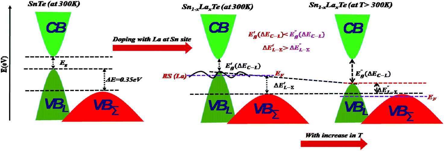
SnTe is a narrow bandgap (p-type) (∼0.18 eV) that belongs to the IV–VI family semiconductor.17 Analogous to PbTe, SnTe exhibits two valence bands (VB) (L and Σ). However, the large energy separation (ΔE = 0.35 eV)18–20 between the light and heavy holes inhibit the Σ band to contribute to the transport properties at room temperature whereas, at high temperature, the L band moves toward the Σ band, and thus band convergence occurs.18–23 Pei et al. have explained explicitly that in the two-valence band model of PbTe, the energy offset between conduction band (CB) and L-band of VB is temperature-dependent. However, the energy offset between CB and the heavy Σ band of VB is independent of temperature but moves gradually with the addition of the dopants.24 Guo et al. elucidated that the L valence band of SnTe is dominated by the antibonding state of Sn-s and Te-p orbitals. However, any addition of dopants weakens the strength of the antibonding state of pristine SnTe leading to the decrease in the energy offset between L- and Σ-valence bands. Thus, doping may induce a band convergence effect in SnTe.25 Fortunately, band convergence is beneficial as it increases the density of state effective mass ( ) of bands near the Fermi level EF and improves the Seebeck coefficient significantly.26,27 On the other hand, yet another effect known as the resonance effect may be induced at room temperature when doped with certain elements as the impurity states are created by dopants near the EF which fall either above the conduction band (CB) edge or below the valence band (VB) edge.14 As this state has the same energy as an extended state, the two states resonate to build up to two extended states of slightly different energies; these, in turn, will have the same energies as other extended states with whom they will resonate in turn,28 and so on as shown in Fig. 1. Thus, the resonant state develops a certain width Γ.28 Stoichiometric SnTe is a p-type semiconductor with a very high carrier concentration resulting from an extremely large number of Sn lattice vacancies, leading to a low Seebeck coefficient.29 Moreover, large energy separation between its light and heavy hole bands, ΔE = 0.3–0.4 eV at room temperature, significantly suppresses the contribution of heavy holes to the Seebeck coefficient at high temperatures. Zhou et al. calculated the light and heavy valence band properties as a function of chemical potential using full generalized Fermi integrals.30 The light band was assumed to be a nonparabolic, Kane band, with a non-parabolicity parameter, β, given by,
  , where Eg was assumed to be constant at 0.18 eV, while the heavy band was modeled as a parabolic band. However, transport properties can be tailored by optimizing the carrier concentration using suitable dopants. Thus, numerous attempts have been made to modify the valence band structure of SnTe resulting in a high zT value.31 Zhang et al. registered a resonant frequency below the SnTe Fermi level that was caused by indium doping and observed a significant rise in the Seebeck coefficient.32 However, Tan et al. indicated that doping should be optimized because with the increase in the doping level, the overall s–p antibonding state is enhanced and thus the resonant level is shifted upward. Consequently, the band convergence effect is hindered.33 Although the concept of valence band convergence in PbTe with increasing temperature and modification of the band structure in PbTe with a sharp peak in the density-of-states (DOS) using La as the dopant, which might be considered as a resonant state, was recognized earlier,34 using the same analogy, the current study involves doping of SnTe using La35 which considerably enhances the thermoelectric performance using two successive approaches.
 |
| | Fig. 1 Schematic band structure of SnTe and La doped SnTe at 300 K and at high temperature. | |
To the best of the knowledge, there is no report available on the solid solution synthesis of Sn1−xLaxTe for enhancing the thermoelectric performance. Here we have investigated the Sn1−xLaxTe (x = 0, 0.04, 0.06, and 0.08) compound by a vacuum melting method followed by the spark plasma sintering (SPS). Employing the current methodology, the device zT ∼ 0.17 at 823 K has been observed with increasing La content in Sn0.92La0.08Te, which is about 88% higher than the value 0.09 at 775 K of pristine SnTe. The device zT calculated for Sn0.94La0.06Te and Sn0.92La0.08Te are close to each other.
2. Experimental procedure
2.1 Starting materials
Chemicals were used as obtained: Sn chunk (99.9999%, Sigma Aldrich), Te shot (99.999%, 5 N, Sigma Aldrich), and lanthanum metal (99.999%, 5 N, Alfa aesar).
2.2 Synthesis
High-purity single elements Sn, Te, and La were weighed according to the stoichiometric compositions of Sn1−xLaxTe (x = 0, 0.04, 0.06, and 0.08) and then put inside 13 mm diameter fused quartz tubes. The tubes were sealed under a vacuum (∼10−4 torr) and slowly heated to 1223 K at 50 K per hour followed by rocking for 5 hours to form a uniform composition and then soaked for 10 h for complete homogenization. The ampoules were then slowly cooled to room temperature at a rate of 70 K per hour. The obtained ingots were then crushed and ground into powders inside the glove box (<1 ppm oxygen level) using a mortar pestle for compaction. The ground powders were filled into a 12 mm diameter graphite die and sintered by spark plasma sintering (SPS, M/s SPS Syntex, 725, Japan) at 773 K for Sn1−xLaxTe (x = 0 and 0.04) and 823 K for Sn1−xLaxTe (x = 0.06 and 0.08) by maintaining a soaking time of 5 minutes under 40 MPa load with a vacuum 10 Pa. Also, during SPS, the DC pulse ratio (current on/off time in milliseconds) 12![[thin space (1/6-em)]](https://www.rsc.org/images/entities/char_2009.gif) :2 has been maintained with a high heating rate of 200 °C min−1.
:2 has been maintained with a high heating rate of 200 °C min−1.
2.3 X-ray diffraction and electron microscopy
The before and after sintered pellets were characterized by X-ray diffraction (XRD) technique Proto AXRD Benchtop Powder diffractometer), under ambient conditions using CuKα radiation (λ = 1.5418 Å). Furthermore, a scanning electron microscope (SEM, M/s JEOL IT300 operated at 15 kV) is used to study the morphological studies and the attached EDS analyzer (M/s EDAX-Octane) is used for elemental analysis and mapping. The transmission electron microscope (JEOL JEM2100F) specimens were created by dispersing the specimen powder onto a copper grid.
2.4 Electrical transport properties
The obtained spark plasma sintered (SPS)-processed pellets were cut into bars with dimensions of 12 mm × 3 mm × 3 mm that was used for simultaneous measurement of the Seebeck coefficient and the electrical conductivity using M/s Linseis LSR-3 instrument under a helium atmosphere from room temperature to 823 K. No hysteresis was seen in heating and cooling cycles. Electrical properties measured for different slices cut from the same pellets were similar, corroborating the homogeneity of the samples. The uncertainty of the Seebeck coefficient and electrical conductivity measurements is ±3%.
2.5 Thermal conductivity
Highly dense SPS-processed pellets of diameter 12 mm were polished for thermal diffusivity measurements. The samples were coated with a thin layer of graphite to minimize errors from the emissivity of the material. The thermal conductivity was calculated from κ = D × Cp × ρ, where the thermal diffusivity coefficient (D) was measured using the laser flash diffusivity method in a Linseis, LFA-1000, the specific heat capacity (Cp) was determined by eqn (2),30| | 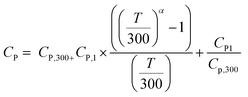 | (2) |
where T is the absolute temperature and CP,300 is the specific heat capacity at 300 K. For SnTe, CP,300 is 0.1973 J g−1 K−1, CP1 is 0.115 J g−1 K−1, and α is 0.63 and the density (ρ) was determined using the dimensions and mass of the sample and found to be >98% of its theoretical density.29 The thermal diffusivity data were analyzed using a Cowan model with pulse correction. The uncertainties in transport and other measurements are ±6% for D, ±3% for σ, ±3% for S, ±10% for Cp and ±0.5% for ρ. Unless otherwise mentioned, all the properties described in this study were measured perpendicular to the sintering pressure direction, although no directional anisotropy effects were perceived in the charge transport properties.
3. Results and discussion
3.1 Structural characterization
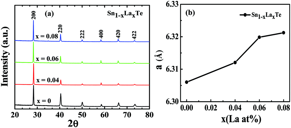
As synthesized Sn1−xLaxTe (x = 0, 0.04, 0.06, and 0.08) were initially characterized by employing XRD to confirm the crystallite size and phase purity. The presence of multiple peaks in the XRD plot suggests the sample is polycrystalline. The Fig. 2(a) of Sn1−xLaxTe (x = 0, 0.04, 0.06, and 0.08) samples were in good agreement with the standard data (JCPDF 08-0487) confirming the phase purity. It is to be noted that all the Bragg's reflections of samples correspond to SnTe which indicates the occupancy of La in the Sn-site in the lattice. No secondary phases were detected in XRD. Besides, all the samples represent the cubic structure with a space group: Fm![[3 with combining macron]](https://www.rsc.org/images/entities/char_0033_0304.gif) m. Lattice parameters were calculated for the samples and it was found that due to the occupancy of La3+ into Sn2+, the stress so developed causes an increase in the lattice parameter. From Fig. 2(b), it has been observed that when concentration was plotted against the lattice parameter obtained from the XRD plot, there is a volume expansion in the lattice with increasing La concentration. However, the change in the lattice parameter shows a negligible change (deviation from Vegard's law type behavior) as the content reaches 8 at%. Thus, the increase in the lattice parameter is expected up to the solubility limit of La in SnTe and a similar kind of behavior is observed earlier for other state-of-the-art thermoelectric materials.10 Generally, if La3Te4 were forming solid solutions with SnTe, one would expect a perpetual Vegard's law type behavior, showing a systematic increase in the band gap with the La3Te4 amount (Eg,La3Te4 ∼ 0.95 eV). The increase in the band-gap is observed only up to 6 at% fractions. It suggests that for La, >6 at% it is excluded from the SnTe matrix. Collectively, both the lattice parameter and band-gap variations suggest that the solubility limit is somewhere around 6 at%.
m. Lattice parameters were calculated for the samples and it was found that due to the occupancy of La3+ into Sn2+, the stress so developed causes an increase in the lattice parameter. From Fig. 2(b), it has been observed that when concentration was plotted against the lattice parameter obtained from the XRD plot, there is a volume expansion in the lattice with increasing La concentration. However, the change in the lattice parameter shows a negligible change (deviation from Vegard's law type behavior) as the content reaches 8 at%. Thus, the increase in the lattice parameter is expected up to the solubility limit of La in SnTe and a similar kind of behavior is observed earlier for other state-of-the-art thermoelectric materials.10 Generally, if La3Te4 were forming solid solutions with SnTe, one would expect a perpetual Vegard's law type behavior, showing a systematic increase in the band gap with the La3Te4 amount (Eg,La3Te4 ∼ 0.95 eV). The increase in the band-gap is observed only up to 6 at% fractions. It suggests that for La, >6 at% it is excluded from the SnTe matrix. Collectively, both the lattice parameter and band-gap variations suggest that the solubility limit is somewhere around 6 at%.
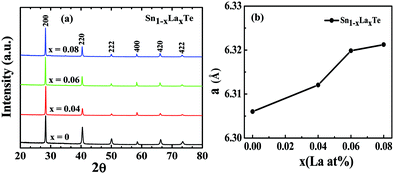 |
| | Fig. 2 (a) X-Ray diffraction patterns of Sn1−xLaxTe (x = 0, 0.04, 0.06, and 0.08) samples (b) the lattice parameter of different La contents in SnTe. | |
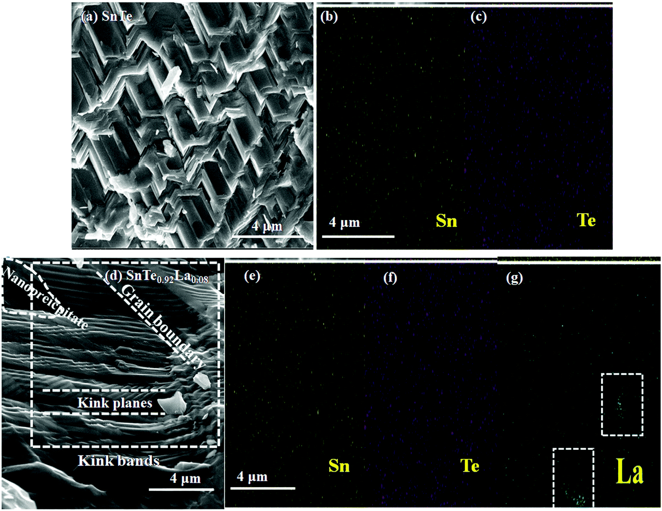
The SEM images revealing the surface morphology of (a) SnTe and (d) Sn0.92La0.08Te samples after SPS are shown in Fig. 3. The image shows that the samples exhibit dense microstructure. The SEM image reveals that kink bands are clearly visible. Moreover, these kink bands have kink planes which are seen up to few microns and are nearly parallel to each other. The uniqueness of the planes is that they are the most active planes for the slip to occur and arises due to the anisotropic growth of the sample.21 The study by Yang et al.36 reported that these kink bands serve as scattering centres for the phonons and thus suppress the thermal conductivity (Fig. 3(d)). Interestingly, a similar kind of morphology is exhibited by all the samples even with increasing La doping in SnTe. However, a nanoprecipitate is seen in the microstructure when the concentration of x = 0.08. This can be attributed to the limited solubility of La in SnTe. This nanoprecipitate is absent in the XRD plot which can be due to the low concentration which is beyond the detection limit. EDS mapping of samples confirm the single-phase compound for Sn1−xLaxTe (x = 0, 0.04 and 0.06). However, from Fig. 3(g), it has been observed that there is a sign of La precipitation in the case of doping when La is present in 8 at%. The EDS spectra of all the compositions of La-doped SnTe, Sn1−xLaxTe (x = 0, 0.04, 0.06 and 0.08) are shown in S1 in the ESI.† The compositional analysis of the nanoprecipitate of Sn0.92La0.08Te is shown in S2 in the ESI.†
 |
| | Fig. 3 SEM with EDX mapping images of (a–c) SnTe, (d–g) Sn0.92La0.08Te samples after SPS. | |
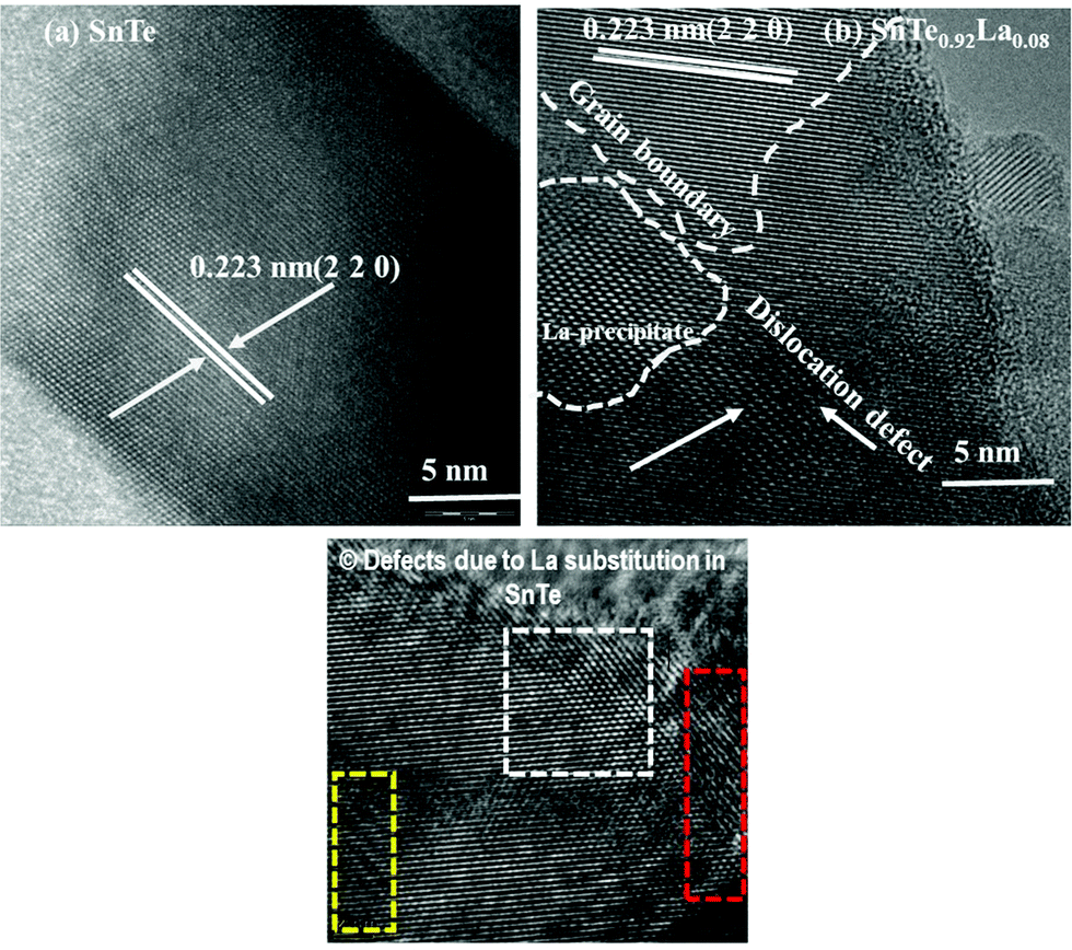
A greater understanding of the morphology of the samples on an atomic scale can be explained by TEM or HRTEM images as shown in Fig. 4(a–c). Pristine SnTe and La-doped SnTe show interplanar spacing, d ∼ 0.223 nm which corresponds to the (2 2 0) plane of rock-salt structure type SnTe.21 The composition Sn0.92La0.08Te shows the presence of grain boundaries, nano-precipitates of La due to the solubility limit and defects although Fig. 4(c) represents that all the three compositions of La-doped SnTe exhibit defects of various length scales and grain boundaries. These grain boundaries along with the defects present in the sample contribute to phonon scattering and thus lattice thermal conductivity is reduced. Thus, the presence of point defects due to the mass defect of Sn and La, La nanoprecipitates, and mesoscale kink bands as discussed earlier scatters the entire spectrum of phonons, thereby reducing the lattice thermal conductivity.
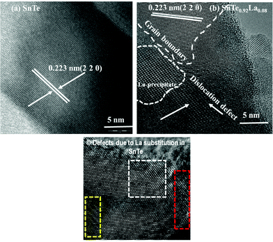 |
| | Fig. 4 TEM images of (a) SnTe, (b) Sn0.92La0.08Te and (c) different types of structural defects present in Sn1−xLaxTe samples after SPS. | |
3.2 Temperature dependent thermoelectric properties
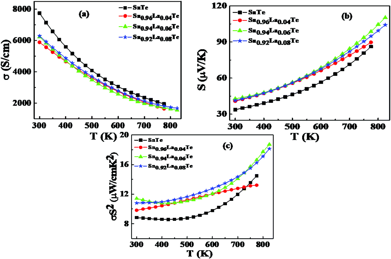
The temperature-dependent thermoelectric properties of La-doped SnTe samples are shown in Fig. 5. The temperature dependence of σ of Sn1−xLaxTe (x = 0, 0.04, 0.06, and 0.08) is shown in Fig. 5(a) and all the samples show the behaviour of degenerate semiconductors where the σ decreases with increase in the temperature. As expected pristine SnTe sample, demonstrates a very high electrical conductivity of ∼7740 mho cm−1 at room temperature due to Sn vacancy concentration. Based on the observation of the σ vs. T plot, where the conductivity value decreases, especially at room temperature from ∼7740 mho cm−1 to ∼5800 mho cm−1 after electron counter-doping, we conclude that La atoms should be a p-type dopant similar to In, Ga, Bi and Sb as electron dopants (counter-doping) which reduces the hole concentration.37 The intrinsic SnTe is p-type due to the Sn vacancies. These vacancies create empty electronic states and thus behave like a p-type dopant. When SnTe was doped with La, the La atoms first fill the “Sn” vacancies. Thus, despite being a p-type dopant, they are not as “robust” as Sn vacancies, in the sense that they induce fewer holes. Thus, at a low doping level, the p-type charge concentration i.e. holes decreases. However, as the doping level increases, at some point, all the Sn vacancies will be filled by La and beyond that point, excess La atoms substitute for Sn and the p-type charge carrier will again start increasing. However, when the solubility limit of La in SnTe will be achieved, the excess La atom will get precipitated and acts as a donor which will thus subsequently decrease the hole carrier concentration. The fact that the electrical conductivity decreases all the way indicates that the La atoms affected the hole mobility significantly and can be attributed to increased effective mass and scattering due to impurities.32
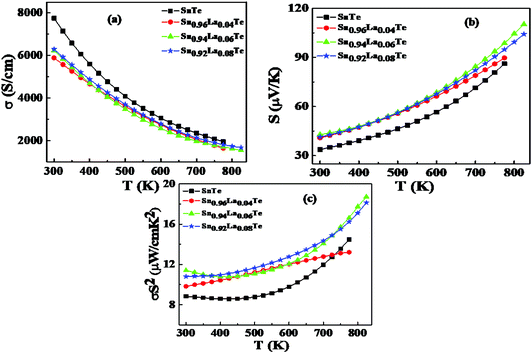 |
| | Fig. 5 Temperature dependence of (a) electrical conductivity, (b) Seebeck coefficient and (c) power factor for Sn1−xLaxTe (x = 0, 0.04, 0.06, and 0.08). | |
The temperature-dependent S for all samples is shown in Fig. 5(b). All the samples exhibit a positive Seebeck coefficient value which indicates p-type conduction in the temperature range of 300 to 823 K. No bipolar conduction was apparent even up to 823 K, in all the compositions despite having a small band-gap of 0.18 eV for SnTe. For all the samples, the Seebeck coefficient maxima shift to higher temperatures with rising La-fraction, but no Seebeck coefficient saturation (i.e. onset of bipolar diffusion) was observed. This observation is consistent with the relationships of band gap (Eg) and the temperature Tmax at which Smax occurs (eqn (3)):10
where
e is the electron charge and the plot is shown in S3 in the ESI.
† The downturn in the Seebeck coefficient at high temperature is widely observed in V
2–VI
3 and IV–VI (V = Bi, Sb; IV = Ge, Sn, Pb; VI = S, Se, Te) narrow gap thermoelectric systems. These bipolar effects degrade the Seebeck coefficients because the thermally excited minority carriers have Seebeck coefficients of the opposite sign and offset those of the majority ones. Therefore, bipolar effects limit the z
T at higher temperatures. However, the bipolar effect in SnTe-based thermoelectric materials as reflected in the Seebeck coefficient (
Fig. 5(b)) is not pronounced as in PbQ and V
2–VI
3 systems because of the very high hole concentration (majority carriers) of SnTe, which is similar to GeTe.
38 The room temperature
S for pristine SnTe is ∼32 μV K
−1 which increased to ∼45 μV K
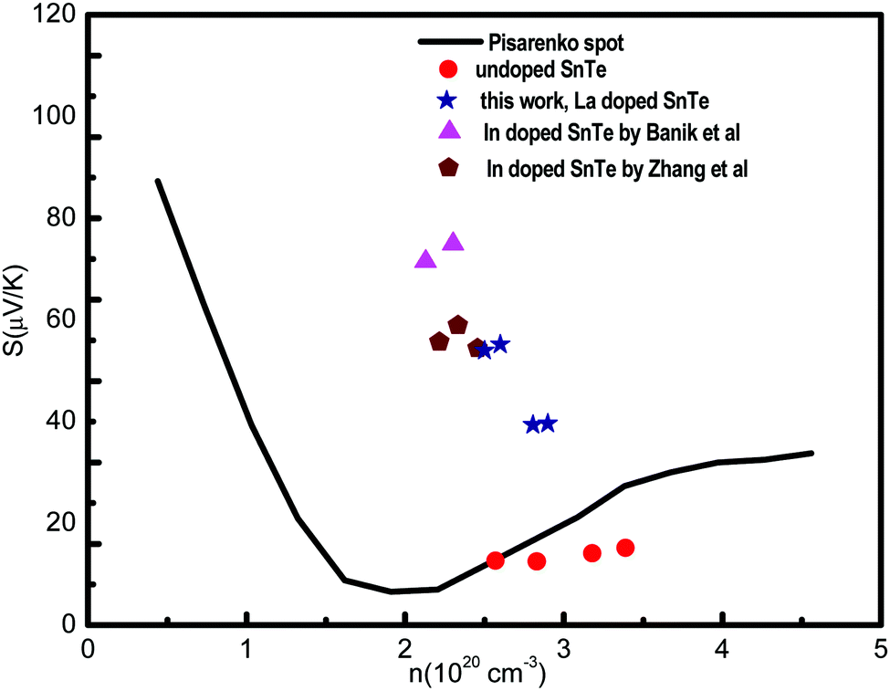
−1 for La-doped samples although the value of the Seebeck coefficient changes negligibly with the concentration of La atoms. The enhancement is 40% over pristine SnTe. This is attributed to the fact that analogous to the In doped SnTe which introduces resonant levels, La-doped SnTe introduces a Fermi level near the edge of the valence band. This is possible due to the interaction of the energetical proximity of the 6s orbital of the La atom and the 5p orbital of Te atom. These two orbitals hybridize to form an s-p antibonding state. As a result, the electronic density of states near the top of the valence band is significantly increased, thereby enhancing the Seebeck coefficient at room temperature. Furthermore, we have shown the room temperature Pisarenko plot
S (shown in
Fig. 6) of La-doped SnTe (our work) as a function of carrier concentration to clarify the origin of the enhanced Seebeck coefficient. The solid curve was calculated on the basis of two parabolic band models as described by Zhang
et al.32 The valence band model (VBM) takes into account the non-parabolicity of the light hole band (L-band) and provides a best quantitative fit to all the Seebeck coefficient values, expect for the In-doped or La-doped samples whose deviation implies an alternative mechanism through which the band structure of pure SnTe near the band edge is altered and one possible mechanism is the introduction of resonance levels.
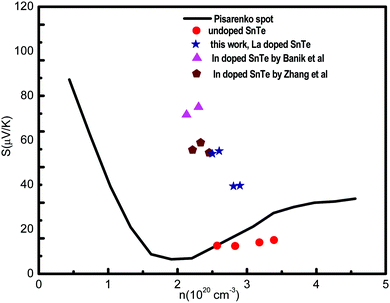 |
| | Fig. 6 Room temperature Seebeck coefficient as a function of carrier concentration of the present Sn-based samples. The solid line is a Pisarenko plot at 300 K computed using the two-valence band model. The experimental data on undoped SnTe,32 In-doped SnTe by Zhang et al.32 and Banik et al.39 are in the inset for comparison. | |
However, at high temperatures, the increase in the Seebeck coefficient is not very prominent between the pristine SnTe snd the La-doped SnTe. This is because resonance levels are known for their ability to enhance the density-of-states and thus the Seebeck coefficient only near room temperature. Furthermore, as discussed earlier, at a higher temperatures, the Fermi energy level is lowered and pushed deeper into the valence band of SnTe which in turn mitigates the phenomenon of the resonance effect, meanwhile facilitating the participation of the heavy hole band, although partially, in the carrier transport.38 Here, the enhancement in the Seebeck effect at high temperatures, essentially the heavy hole, Σ band contributes at high temperature once the Sn-vacancies are removed substantially. This phenomenon opens the band gap and diminishes the band offset between the light valence band (L-band) and the heavy valence band (Σ-band). The band-gap enlargement reduces the minority charge carriers at elevated temperature and suppresses the bipolar diffusion, i.e. the material is eligible for thermoelectric applications for a wider range of temperature.38 Since, at high temperature, the increase in the Seebeck coefficient is not very high for La-doped SnTe samples as compared to Hg/Cd/Mn/Mg/Ca doped SnTe, it can be assumed that the La-doping in SnTe pushes the Pisarenko plot to region II, where the heavy valence band (Σ-band) contributes partially alongwith the L-band in the transport properties.37 Thus, according to Kane-band theory, the conduction band edge and the valence band edges in SnTe are at the L-point, with a narrow band-gap of 0.18 eV. The small energy gap causes a highly non-parabolic light hole band with a small band edge density of states (DOS) effective mass of m* ∼ 0.168me. This narrow energy gap is also a probable reason for the introduction of resonance state upon doping. Moreover, a flatter, heavy-mass region of the valence band lies below the valence band edge, with the energy difference between the light-hole and heavy-hole maxima estimated to be in the range of ΔE ∼ 0.3–0.4 eV with an effective mass of ∼1.92me.18Fig. 5(c) shows the temperature dependence of the power factor for Sn1−xLaxTe (x = 0, 0.04, 0.06 and 0.08) samples. It can be seen that the La-doped samples exhibit a higher power factor over a very broad temperature range because of the largely improved Seebeck coefficient. The power factor enhancement to 11.5 μW cm−1 K−2 at 300 K for La-doped samples (x ≥ 0.06) is highest and the increase is 35% in comparison to the pristine SnTe. The highest power factor of 19 μW cm−1 K−2 was achieved at 823 K for Sn0.94La0.06Te which is comparable with the other doped SnTe samples having high zT values.39 Moreover, this is the highest power factor value achieved compared to other reported values for lanthanides.40
3.3 Thermal transport properties
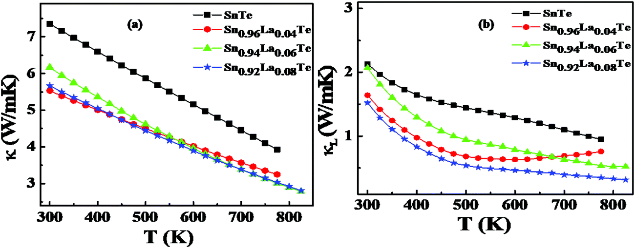
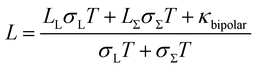
The total thermal conductivity, κtotal and the calculated lattice thermal conductivity, κL of Sn1−xLaxTe (x = 0, 0.04, 0.06, and 0.08) samples are shown in Fig. 7(a and b). The overall thermal conductivity at room temperature is decreased from ∼7.5 W m−1 K−1 for pristine SnTe to ∼5.5 W m−1 K−1 for Sn0.96La0.04Te. The thermal conductivities of all the La-doped samples are lower than that of the undoped SnTe which comes from the reduction of the electronic part of the thermal conductivity (due to the decrease in the hole concentration.30 The electronic contribution of the thermal conductivity is given by Wiedemann–Franz law, Where T is the absolute temperature, σ is the electrical conductivity, and L is the Lorenz number.
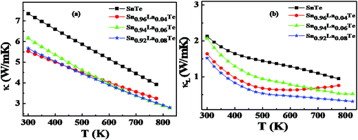 |
| | Fig. 7 Temperature-dependent (a) and (b) of Sn1−xLaxTe (x = 0, 0.04, 0.06, and 0.08) samples. | |
For the two-band model, L is estimated as ((eqn (4) and (5))
| |  | (4) |
where,
| |  | (5) |
The above equation includes only bipolar effects within the two valence bands—electron–hole bipolar effects (most commonly thought of) are not considered in this Lorenz number calculation.30 However, due to the non-parabolicity and complexity of the valence band structure around the Fermi level for p-type SnTe, the exact determination of L is difficult. An estimation of L can be made using a single parabolic band (SPB) model considering acoustic phonon scattering, resulting in L with a deviation of less than 10% as compared with a more rigorous single non-parabolic band and multiple band model calculations.30 However, if we carefully observe the reduction in the total thermal conductivity due to La-doping, the reduction effect is weakened at high temperature. The κlat conductivity at high temperature is determined mainly by a large number of low wavelength phonons. It is well-known that low wavelength phonons are mostly scattered by the atomic scale point defects due to mass and strain field fluctuations. For the alloys with point defects, the scattering factor (A) could be expressed by the following eqn (6) when the measuring temperature is beyond 650 K.41
| |  | (6) |
where
Ω0,
ν,
x, Δ
M,
M are the volume of the unit cell, the lattice sound velocity, the fraction of guest atom, the atomic mass difference between the guest and the host, and the average mass of the cell, respectively. The higher the atomic mass difference between the doping atoms and the host atoms (Δ
M) is, the larger the value of Δ
M/M would be and thus the smaller is the lattice thermal conductivity. Thus, all the La-doped samples exhibit low lattice thermal conductivity in comparison to the pristine SnTe, due to the reasonably high atomic mass unit (a.m.u.) difference of La (a.m.u. of La = 138.905) and Sn (a.m.u. of Sn = 118.71). Moreover, it is also seen that La (
x = 0.08) shows the least
κlat value.
Finally, it is confirmed that the κtotal of La-doped SnTe samples are significantly suppressed in comparison to the pristine SnTe. The reduction of κtotal is mainly attributed to the mass fluctuation caused by point defects and grain boundaries scattering as reported for other thermoelectric materials and7,22,29 the same is evident from Fig. 7(b).
The thermoelectric zT is calculated using the measured σ, S and κtotal. Fig. 8 shows the temperature-dependent of thermoelectric zT of Sn1−xLaxTe (x = 0, 0.04, 0.06 and 0.08). The samples showed a systematic increase in zT with increasing La content in SnTe at room temperature. The zT value of ∼0.6 at 823 K has been obtained for Sn0.94La0.06Te, which is ∼96% higher than the value 0.28 at 775 K of pristine SnTe and this value is higher than the reported value of other lanthanides (Sn0.94Gd0.06Te and Sn49.25Te49.25Eu1.5).40,42
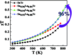 |
| | Fig. 8 Temperature dependent zT of Sn1−xLaxTe (x = 0 to 0.08). | |
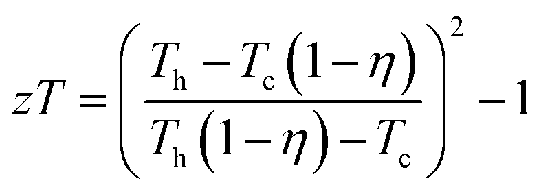
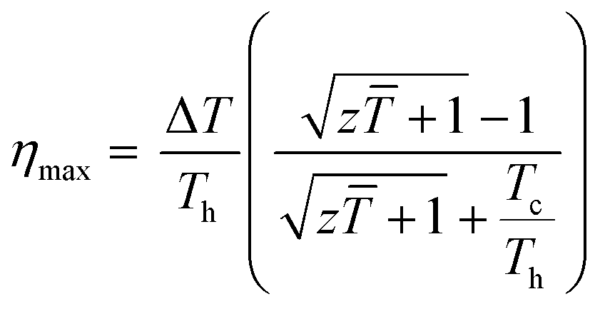
Finally, the TE device zT was calculated using the equation, given a finite, temperature difference ΔT = Th − Tc, is then defined from the maximum efficiency η of a single thermoelectric leg, is given by eqn (7):
| |  | (7) |
where the maximum conversion efficiency (
η) were estimated by using the
eqn (8):
| |  | (8) |
from the temperature-dependent properties
S(
T),
σ(
T), and
κ(
T) between
Th and
Tc as suggested by Snyder
et al.43 Furthermore,
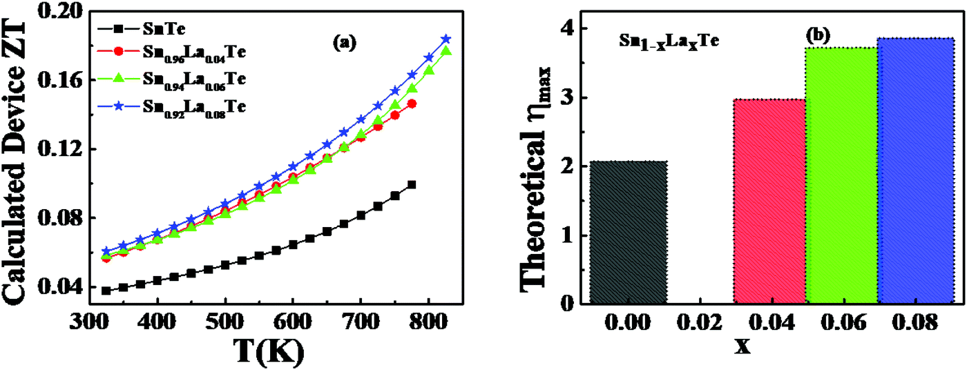
Fig. 9(a) shows the temperature-dependence of calculated device
zT of Sn
1−xLa
xTe (
x = 0 to 0.08) and all the samples have shown a systematic improvement of device
zT with increasing La content in SnTe. Finally, the device
zT value of 0.17 at 823 K has been obtained for Sn
0.92La
0.08Te, which is ∼88% higher than the value 0.09 at 775 K of pristine SnTe. The exact calculation of maximum efficiency is explained in the spreadsheet S.4.1 to S.4.4 for download in the ESI.
† Also,
Fig. 9(b) represents the theoretical maximum conversion efficiency of La-doped SnTe samples. Moreover, all the samples have shown a systematic increase in conversion efficiency with increasing La content in SnTe. Finally, the maximum conversion efficiency has been observed to be increased from 2.0 to 3.7% for Sn
0.92La
0.08Te. The significant improvement in device efficiency is encouraging for considering these materials as a suitable alternative to Pb-based chalcogenides.
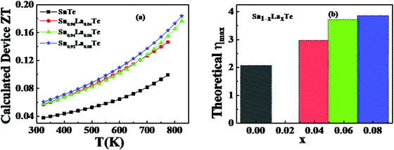 |
| | Fig. 9 (a) Temperature-dependent calculated device zT (b) Theoretical maximum conversion efficiency in percentage. | |
4. Conclusions
In summary, La-doped SnTe samples are successfully synthesized by vacuum melting. The synthesized samples have shown a maximum solubility of 6 at% La in SnTe; beyond that La, gets precipitated which was confirmed by microstructural investigations by SEM and TEM. Furthermore, the enhancement of the Seebeck coefficient and power factor for La-doped SnTe was proposed to be due to the creation of resonance states where the Fermi level lies in the valence band at room temperature. However, at high temperature the participation of the heavy valence band in the transport properties, and the presence of defects of all length scale which significantly enhances the phonon scattering resulted in the zT value of ∼0.6 at 823 K for Sn0.94La0.06Te, which is ∼96% higher for pristine SnTe. Also, the device zT value of 0.17 at 823 K was obtained for Sn0.92La0.08Te, which is ∼88% higher than the value 0.09 at 773 K of pristine SnTe. The current investigation resembles that there is a large scope to enhance thermoelectric performance for SnTe material by using the heavier lanthanide elements.
Conflicts of interest
There is no conflict of interest.
Acknowledgements
FRGS no. GGSIPU/DRC/FRGS/2019/1553/11. The authors sincerely acknowledge Director CSIR-NPL, India, and BRNS (Board of Research in Nuclear Sciences), Department of Atomic Energy for their experimental and financial support (Sanction No. 37(3)/14/22/2016-BRNS India), respectively. The authors from SSSIHL thank the founder Chancellor Bhagawan Sri Sathya Sai Baba and Trustees/Administrators for providing characterization facilities at Central Research Instruments Facility (SSSIHL-CRIF).
References
- Z. Hou, Y. Xiao and L.-D. Zhao, Investigation on carrier mobility when comparing nanostructures and bands manipulation, Nanoscale, 2020, 12, 12741–12747 Search PubMed.
- W. Wunderlich, H. Ohta and K. Koumoto, Enhanced effective mass in doped SrTiO3 and related perovskites, Phys. B, 2009, 404, 2202–2212 Search PubMed.
-
D. M. Rowe, CRC handbook of thermoelectrics, CRC Press, 2018 Search PubMed.
- Z. M. Gibbs, F. Ricci, G. Li, H. Zhu, K. Persson and G. Ceder,
et al., Effective mass and Fermi surface complexity factor from ab initio band structure calculations, npj Comput. Mater., 2017, 3, 8 Search PubMed.
-
S. Kasap, C. Koughia and H. E. Ruda, Electrical conduction in metals and semiconductors, Springer Handbook of Electronic and Photonic Materials, Springer, 2017, p. 1 Search PubMed.
-
K. Hess, Advanced theory of semiconductor devices, 2000 Search PubMed.
- S. Bhattacharya, A. Bohra, R. Basu, R. Bhatt, S. Ahmad, K. N. Meshram, A. K. Debnath, S. K. Sarkar, M. Navaneethan, Y. Hayakawa, D. K. Aswal and S. K. Gupta, High thermoelectric performance of (AgCrSe2)0.5(CuCrSe2)0.5 nano-composites having all-scale natural hierarchical architectures., J. Mater. Chem. A, 2014, 2, 17122–17129 Search PubMed.
- R. Basu, S. Bhattacharya, R. Bhatt, M. Roy, S. Ahmad, A. Singh, M. Navaneethan, Y. Hayakawa, D. K. Aswal and S. K. Gupta, Improved thermoelectric performance of hot pressed nanostructured n-type SiGe bulk alloys, J. Mater. Chem. A, 2014, 2, 6922–6930 Search PubMed.
- K. Biswas, J. He, I. D. Blum, C.-I. Wu, T. P. Hogan, D. N. Seidman, V. P. Dravid and M. G. Kanatzidis, High-performance bulk thermoelectrics with all-scale hierarchical architectures, Nature, 2012, 489, 414–418 Search PubMed.
- L.-D. Zhao, H. Wu, S. Hao, C.-I. Wu, X. Zhou, K. Biswas, J. He, T. P. Hogan, C. Uher, C. Wolverton, V. P. Dravid and M. G. Kanatzidis, All-scale hierarchical thermoelectrics: MgTe in PbTe facilitates valence band convergence and suppresses bipolar thermal transport for high performance, Energy Environ. Sci., 2013, 6, 3346–3355 Search PubMed.
- G. Tan, F. Shi, S. Hao, H. Chi, T. P. Bailey, L.-D. Zhao, C. Uher, C. Wolverton, V. P. Dravid and M. G. Kanatzidis, Valence Band Modification and High Thermoelectric Performance in SnTe Heavily Alloyed with MnTe, J. Am. Chem. Soc., 2015, 137, 11507–11516 Search PubMed.
- Z. Ma, C. Wang, Y. Chen, L. Li, S. Li, J. Wang and H. Zhao, Ultra-high thermoelectric performance in SnTe by the integration of several optimization strategies, Mater. Today Phys., 2021, 17, 100350 Search PubMed.
- R. Moshwan, W.-D. Liu, X.-L. Shi, Y.-P. Wang, J. Zou and Z.-G. Chen, Realizing high thermoelectric properties of SnTe via synergistic band engineering and structure engineering, Nano Energy, 2019, 65, 104056 Search PubMed.
- D. K. Bhat and U. S. Shenoy, Zn: a versatile resonant dopant for SnTe thermoelectrics, Mater. Today Phys., 2019, 11, 100158 Search PubMed.
- R. D. Schmidt, E. D. Case, J. E. Ni, R. M. Trejo, E. Lara-Curzio, R. J. Korkosz and M. G. Kanatzidis, High-temperature elastic moduli of thermoelectric SnTe1±x–ySiC nanoparticulate composites, J. Mater. Sci., 2013, 48, 8244–8258 Search PubMed.
- A. Banik, U. S. Shenoy, S. Anand, U. V. Waghmare and K. Biswas, Mg Alloying in SnTe Facilitates Valence Band Convergence and Optimizes Thermoelectric Properties, Chem. Mater., 2015, 27, 581–587 Search PubMed.
- X. J. Tan, H. Z. Shao, J. He, G. Q. Liu, J. T. Xu, J. Jiang and H. C. Jiang, Band engineering and improved thermoelectric performance in M-doped SnTe (M = Mg, Mn, Cd, and Hg), Phys. Chem. Chem. Phys., 2016, 18, 7141–7147 Search PubMed.
- G. Tan, W. G. Zeier, F. Shi, P. Wang, G. J. Snyder, V. P. Dravid and M. G. Kanatzidis, High Thermoelectric Performance SnTe-In2Te3 Solid Solutions Enabled by Resonant Levels and Strong Vacancy Phonon Scattering, Chem. Mater., 2015, 27, 7801–7811 Search PubMed.
- G. Tan, L.-D. Zhao, F. Shi, J. W. Doak, S.-H. Lo, H. Sun, C. Wolverton, V. P. Dravid, C. Uher and M. G. Kanatzidis, High Thermoelectric Performance of p-Type SnTe via a Synergistic Band Engineering and Nanostructuring Approach, J. Am. Chem. Soc., 2014, 136, 7006–7017 Search PubMed.
- S. Ahmad, A. Singh, S. Bhattacharya, M. Navaneethan, R. Basu, R. Bhatt, P. Sarkar, K. N. Meshram, A. K. Debnath, K. P. Muthe and D. K. Aswal, Band Convergence and Phonon Scattering Mediated Improved Thermoelectric Performance of SnTe–PbTe Nanocomposites, ACS Appl. Energy Mater., 2020, 3, 8882–8891 Search PubMed.
- S. Ahmad, A. Singh, S. Bhattacharya, M. Navaneethan, R. Basu, R. Bhatt, P. Sarkar, K. N. Meshram, K. P. Muthe and S. Vitta, Remarkable Improvement of Thermoelectric Figure-of-Merit in SnTe through In Situ-Created Te Nanoinclusions, ACS Appl. Energy Mater., 2020, 3, 7113–7120 Search PubMed.
- D. Sarkar, T. Ghosh, A. Banik, S. Roychowdhury, D. Sanyal and K. Biswas, Highly Converged Valence Bands and Ultralow Lattice Thermal Conductivity for High-Performance SnTe Thermoelectrics, Angew. Chem., Int. Ed., 2020, 59, 11115–11122 Search PubMed.
- J.-W. Zhang, Z.-W. Wu, B. Xiang, N.-N. Zhou, J.-L. Shi and J.-X. Zhang, Ultralow Lattice Thermal Conductivity in SnTe by Incorporating InSb, ACS Appl. Mater. Interfaces, 2020, 12, 21863–21870 Search PubMed.
- Y. Pei, X. Shi, A. LaLonde, H. Wang, L. Chen and G. J. Snyder, Convergence of electronic bands for highperformance bulk thermoelectrics, Nature, 2011, 473, 66–69 Search PubMed.
- F. Guo, B. Cui, H. Geng, Y. Zhang, H. Wu, Q. Zhang, B. Yu, S. J. Pennycook, W. Cai and J. Sui, Simultaneous Boost of Power Factor and Figure-of-Merit in In–Cu Codoped SnTe, Small, 2019, 15, 1902493 Search PubMed.
- A. Doi, S. Shimano, D. Inoue, T. Kikitsu, T. Hirai, D. Hashizume, Y. Tokura and Y. Taguchi, Band engineering, carrier density control, and enhanced thermoelectric performance in multi-doped SnTe, APL Mater., 2019, 7, 091107 Search PubMed.
- X. Guo, Z. Chen, J. Tang, F. Zhang, Y. Zhong, H. Liu and R. Ang, Thermoelectric transport properties in Bi-doped SnTe–SnSe alloys, Appl. Phys. Lett., 2020, 116, 103901 Search PubMed.
- J. P. Heremans, B. Wiendlocha and A. M. Chamoire, Resonant levels in bulk thermoelectric semiconductors, Energy Environ. Sci., 2012, 5, 5510–5530 Search PubMed.
- M. Zhou, G. J. Snyder, L. Li and L.-D. Zhao, Lead-free tin chalcogenide thermoelectric materials, Inorg. Chem. Front., 2016, 3, 1449–1463 Search PubMed.
- M. Zhou, Z. M. Gibbs, H. Wang, Y. Han, C. Xin, L. Li and G. J. Snyder, Optimization of thermoelectric efficiency in SnTe: the case for the light band, Phys. Chem. Chem. Phys., 2014, 16, 20741–20748 Search PubMed.
- X. Chen, D. Parker and D. J. Singh, Importance of non-parabolic band effects in the thermoelectric properties of semiconductors, Sci. Rep., 2013, 3, 1–6 Search PubMed.
- Q. Zhang, B. Liao, Y. Lan, K. Lukas, W. Liu, K. Esfarjani, C. Opeil, D. Broido, G. Chen and Z. Ren, High thermoelectric performance by resonant dopant indium in nanostructured SnTe, Proc. Natl. Acad. Sci. U. S. A., 2013, 110, 13261–13266 Search PubMed.
- X. Tan, X. Tan, G. Liu, J. Xu, H. Shao, H. Hu, M. Jin, H. Jiang and J. Jiang, Optimizing the thermoelectric performance of In–Cd codoped SnTe by introducing Sn vacancies, J. Mater. Chem. C, 2017, 5, 7504–7509 Search PubMed.
- X. Tan, G. Liu, J. Xu, X. Tan, H. Shao, H. Hu, H. Jiang, Y. Lu and J. Jiang, Thermoelectric properties of In–Hg co-doping in SnTe: Energy band engineering, J. Materiomics, 2018, 4, 62–67 Search PubMed.
- Q. Yang, T. Lyu, Z. Li, H. Mi, Y. Dong, H. Zheng, Z. Sun, W. Feng and G. Xu, Realizing widespread resonance effects to enhance thermoelectric performance of SnTe, J. Alloys Compd., 2021, 852, 156989 Search PubMed.
- L. Yang, Q. Zhang, Z. Wei, Z. Cui, Y. Zhao, T. T. Xu, J. Yang and D. Li, Kink as a New Degree of Freedom to Tune the Thermal Conductivity of Si Nanoribbons, J. Appl. Phys., 2019, 126, 155103 Search PubMed.
- L.-D. Zhao, X. Zhang, H. Wu, G. Tan, Y. Pei, Y. Xiao, C. Chang, D. Wu, H. Chi and L. Zheng, Enhanced thermoelectric properties in the counter-doped SnTe system with strained endotaxial SrTe, J. Am. Chem. Soc., 2016, 138, 2366–2373 Search PubMed.
- H. Wu, C. Chang, D. Feng, Y. Xiao, X. Zhang, Y. Pei, L. Zheng, D. Wu, S. Gong and Y. Chen, Synergistically optimized electrical and thermal transport properties of SnTe via alloying high-solubility MnTe, Energy Environ. Sci., 2015, 8, 3298–3312 Search PubMed.
- A. Banik, S. Roychowdhury and K. Biswas, The journey of tin chalcogenides towards high-performance thermoelectrics and topological materials, Chem. Commun., 2018, 54, 6573–6590 Search PubMed.
- X. Wang, K. Guo, I. Veremchuk, U. Burkhardt, X. Feng, J. Grin and J. Zhao, Thermoelectric properties of Eu- and Na-substituted SnTe, J. Rare Earths, 2015, 33, 1175–1181 Search PubMed.
- Z. Ma, C. Wang, J. Lei, D. Zhang, Y. Chen, J. Wang, Z. Cheng and Y. Wang, High Thermoelectric Performance of SnTe by the Synergistic Effect of Alloy Nanoparticles with Elemental Elements, ACS Appl. Energy Mater., 2019, 2, 7354–7363 Search PubMed.
- L. Zhang, J. Wang, Z. Cheng, Q. Sun, Z. Li and S. Dou, Lead-free SnTe-based thermoelectrics: enhancement of thermoelectric performance by doping with Gd/Ag, J. Mater. Chem. A, 2016, 4, 7936–7942 Search PubMed.
- G. J. Snyder and A. H. Snyder, Figure of merit ZT of a thermoelectric device defined from materials properties, Energy Environ. Sci., 2017, 10, 2280–2283 Search PubMed.
Footnote |
| † Electronic supplementary information (ESI) available. See DOI: 10.1039/d1ma00155h |
|
| This journal is © The Royal Society of Chemistry 2021 |
Click here to see how this site uses Cookies. View our privacy policy here. 
 Open Access Article
 This Open Access Article is licensed under a Creative Commons Attribution-Non Commercial 3.0 Unported Licence
 *b,
B.
Khasimsaheb
c,
Sivaiah
Bathula
de,
Sai
Muthukumar V.
f,
Ajay
Singh
b and
S.
Neeleshwar
a
*b,
B.
Khasimsaheb
c,
Sivaiah
Bathula
de,
Sai
Muthukumar V.
f,
Ajay
Singh
b and
S.
Neeleshwar
a
 ) of bands near the Fermi level EF and improves the Seebeck coefficient significantly.26,27 On the other hand, yet another effect known as the resonance effect may be induced at room temperature when doped with certain elements as the impurity states are created by dopants near the EF which fall either above the conduction band (CB) edge or below the valence band (VB) edge.14 As this state has the same energy as an extended state, the two states resonate to build up to two extended states of slightly different energies; these, in turn, will have the same energies as other extended states with whom they will resonate in turn,28 and so on as shown in Fig. 1. Thus, the resonant state develops a certain width Γ.28 Stoichiometric SnTe is a p-type semiconductor with a very high carrier concentration resulting from an extremely large number of Sn lattice vacancies, leading to a low Seebeck coefficient.29 Moreover, large energy separation between its light and heavy hole bands, ΔE = 0.3–0.4 eV at room temperature, significantly suppresses the contribution of heavy holes to the Seebeck coefficient at high temperatures. Zhou et al. calculated the light and heavy valence band properties as a function of chemical potential using full generalized Fermi integrals.30 The light band was assumed to be a nonparabolic, Kane band, with a non-parabolicity parameter, β, given by,
  , where Eg was assumed to be constant at 0.18 eV, while the heavy band was modeled as a parabolic band. However, transport properties can be tailored by optimizing the carrier concentration using suitable dopants. Thus, numerous attempts have been made to modify the valence band structure of SnTe resulting in a high zT value.31 Zhang et al. registered a resonant frequency below the SnTe Fermi level that was caused by indium doping and observed a significant rise in the Seebeck coefficient.32 However, Tan et al. indicated that doping should be optimized because with the increase in the doping level, the overall s–p antibonding state is enhanced and thus the resonant level is shifted upward. Consequently, the band convergence effect is hindered.33 Although the concept of valence band convergence in PbTe with increasing temperature and modification of the band structure in PbTe with a sharp peak in the density-of-states (DOS) using La as the dopant, which might be considered as a resonant state, was recognized earlier,34 using the same analogy, the current study involves doping of SnTe using La35 which considerably enhances the thermoelectric performance using two successive approaches.