
 Open Access Article
 This Open Access Article is licensed under a Creative Commons Attribution-Non Commercial 3.0 Unported Licence
Incorporation of porous protective layers as a strategy to improve mechanical stability of Tamm plasmon based detectors†
Josefina
Morrone‡
 a,
Juan Ignacio
Ramallo‡
ab,
Diego F.
Lionello
ab,
Andrés
Zelcer
c,
Baptiste
Auguié
d,
Paula C.
Angelomé
*a and
M. Cecilia
Fuertes
*a
a,
Juan Ignacio
Ramallo‡
ab,
Diego F.
Lionello
ab,
Andrés
Zelcer
c,
Baptiste
Auguié
d,
Paula C.
Angelomé
*a and
M. Cecilia
Fuertes
*a
aGerencia Química & INN, Centro Atómico Constituyentes, Comisión Nacional de Energía Atómica, CONICET, San Martín, Buenos Aires, Argentina. E-mail: angelome@cnea.gov.ar; mfuertes@cnea.gov.ar
bInstituto Sabato, Comisión Nacional de Energía Atómica – Universidad Nacional de San Martín, San Martín, Buenos Aires, Argentina
cCIBION, CONICET, Ciudad de Buenos Aires, Argentina – ECyT, Universidad Nacional de San Martín, San Martín, Buenos Aires, Argentina
dThe MacDiarmid Institute for Advanced Materials and Nanotechnology – School of Chemical and Physical Sciences, Victoria University of Wellington, PO Box 600, Wellington 6140, New Zealand
First published on 17th March 2021
Abstract
Nanostructures supporting optical modes known as Tamm plasmon-polaritons are a new class of optical devices with promising characteristics for sensing applications. Their synthesis involves the deposition of a thin metallic layer on top of a distributed Bragg reflector. Unfortunately, this metallic layer can be easily detached or scratched during normal handling or under operating conditions. In this work, a new strategy to protect these devices from mechanical stress by adding a porous protective overlayer is presented. Three different mesoporous oxides prepared using a sol–gel process were chosen to cover the device: ZrO2 and Ti–Si mixed oxides functionalized with either vinyl or phenyl groups. The mechanical and tribological properties of each candidate were measured using nanoindentation and its ideal thickness was determined by simulation of the optical response. Finally, the devices were characterized mechanically, to test their stability, and their sensing capabilities were determined for both liquids and vapours. The results indicate that thin mesoporous films used as protective layers provide a clear improvement in the device's resistance towards mechanical stress without compromising the optical and sensing properties. The strategy of protection using a porous top layer presented in this work can be extended to other devices which require interaction with the environment through an exposed unstable surface.
1 Introduction
The scientific community is always looking for the development of reliable and stable sensors that can help to control industrial processes, monitor the environment, detect pathogens and diagnose diseases, among many other relevant technological applications.Among all the available technologies to produce sensors, optical ones have a prominent role. In this kind of sensors, the response is based on changes in optical properties such as absorbance, transmittance or fluorescence, generated by specific or unspecific physical, chemical or biological interactions. Thus, they allow following complex interactions non-intrusively by means of simple instruments or even by the naked eye, a considerable advantage from a technical implementation point of view. Moreover, they can also be miniaturized, and enable remote measurement.1–8
In this direction, sensing devices based on Tamm plasmon-polaritons (TPPs) have emerged in recent years as an interesting alternative or complement to existing systems. TPPs are the result of trapping optical energy at the interface between a metallic thin film and a one-dimensional photonic crystal, or distributed Bragg reflector (DBR).9,10 These TPPs, which can be excited at normal incidence, are sensitive to changes in the refractive index of the photonic crystal. Unlike the photonic band gap, the Tamm modes have a narrow spectral width, making them ideal to obtain highly sensitive optical sensors. These devices have been studied in depth by theoretical methods,11–23 which confirm the feasibility of the approach. There are also some examples in which these theoretical predictions have been confirmed by experiments.9,24–26
The construction of a TPP-based device requires attaching a DBR to a thin noble metal layer. Our group has previously demonstrated that DBRs built from mesoporous oxide thin films and coated with a sputtered Au layer sustain a well-defined Tamm plasmon resonance, and behave as sensors for the detection of both liquids and vapours.9,24
Mesoporous thin films, prepared by the combination of sol–gel chemistry and supramolecular self-assembly, present an excellent combination of robustness, chemical versatility and high porosity. Through an appropriate design, a DBR built from these films is stable against both manipulation and any harsh conditions that may be required during measurements. However, the Au layer deposited on top of the mesoporous DBR is not as robust, particularly in regards to manipulation. This is a key feature for vapor sensors that need to be transported and placed in different areas.
The problems related with the mechanical instability of the Au layer are usually solved using standard Ti or Cr metallic adhesion layers. However, it has been demonstrated that Cr interdiffuses with the Au layer forming a Cr–Au alloy and that both Ti and Cr adhesion layers can be partially oxidized, modifying the optical properties of the devices and the adhesion characteristics of these metallic layers.27 In particular, in TPP devices the Au adhesion problem cannot be solved via standard metallic adhesion layers, as their lossy optical response proves highly-detrimental to the TPP resonance (see simulations in ESI,† Fig. S1). Besides, for sensing applications, the Au film has to present certain porosity or micro-cracks, to allow the analytes transport.24 By using a metallic adhesion layer, this characteristics is lost, as a denser Au film is formed on top. The reverse structure, covering a Au film with a DBR, is a valid alternative to support TPPs, but the synthesis of such devices is much more problematic because the thermal stress developed between the Au and the oxides during the DBR layers consolidation detaches the device from the substrate or produces cracks in its structure.
Our proposed strategy, demonstrated below, is to cover the metallic layer with a protective coating. This approach has been used to protect surfaces and devices from environmental conditions, with antifouling, antireflective, antifogging, superhydrophobic or self-cleaning coatings.28–34 In the case of TPP-based sensors, this protective layer (PL) must meet a number of requirements to work properly. Firstly, it must be mechanically robust, in order to stabilize the metallic layer and prevent its detachment. Moreover, it has to be porous enough to ensure an effective analyte transport towards the sensing zone. Finally, the presence of the PL should not drastically affect the TPP band position and width in order to preserve the analytical performance of the device; thus, a good control over the PL thickness is required. Additionally, since the top-most layer of the device is the one that directly interacts with the medium, it would be also advantageous if this PL could be chemically modified by simple procedures. This would help to increment the sensitivity and/or selectivity of the sensors, both critical considerations for sensing devices relying on unspecific signals such as refractive index change.
Having all these requirements in mind, mesoporous thin films prepared in a similar manner to the films used to build the DBR are an excellent option for the design and construction of PLs. In the first place, the way they are synthesized is fully compatible with the rest of the device's production. Additionally, the chemical and mechanical properties of these films can be easily varied by adequately selecting the precursors for the synthesis. Moreover, their thickness can be tuned, without losing porosity and accessibility.35,36 For mesoporous thin films prepared by Evaporation-Induced Self Assembly (EISA) approach, the final thickness depends on the relative amount of solvent used for the sol preparation.35,37 In particular, ultrathin mesoporous films can be obtained using a high amount of volatile solvent in the precursor solution. Such dilution gives rise to films with thicknesses as low as 5 nm that still present accessible porosity.38,39 Finally, this kind of films can include a wide variety of organic functions either incorporated by co-condensation or post functionalization approaches,40 or by a combination of the two, thanks to click thiol–ene reactions.41,42
The remainder of this manuscript describes the optimization, construction and characterization of functional PLs for Tamm plasmon based sensing devices. In a first step, the ideal thickness of the PLs was predicted using numerical simulations. Afterwards, three different materials were chosen and their mechanical properties were evaluated: mesoporous ZrO2 and mesoporous Ti–Si mixed oxides functionalized with vinyl or phenyl organic groups. Two of these oxides were selected to build the protected sensing devices. Mechanical stability and resistance to manipulation of the devices were tested and compared with the unprotected ones. Finally, the sensing capabilities of the protected devices was assessed.
2 Experimental section
2.1 Construction of the Tamm plasmon devices
Sols prepared for the synthesis of the DBR layers are described in the ESI.† For the synthesis of PLs, three different sols were prepared but, in all cases, non-ionic triblock copolymer Pluronic F127 was used as pore template. As a consequence, the pores of the PLs are larger than or equal to those of the layers forming the DBR (as pores generate using Pluronic F127 are larger than the obtained using Brij58 and CTAB).24
For hybrid films, ethanolic solutions of TiCl4 were prepared and then the rest of the compounds were added in the following order: surfactant, organosilane, water. The final molar ratio was TiCl4![[thin space (1/6-em)]](https://www.rsc.org/images/entities/char_2009.gif) :R-Si(OEt)3:F127:H2O:EtOH 0.8:0.2:0.005:10:40.44 The organic groups R used were vinyl and phenyl; the resulting mixed hybrid oxides were called TSV or TSP, respectively. For the synthesis of zirconia films, a solution of ZrCl4:F127:H2O:EtOH with 1:0.005:20:40 molar ratio was used,45 and the oxide was named ZF. These solutions were used to prepared thick films for structural and mechanical characterization; for the deposition of the different protective layers, the sols previously described were diluted 1:4 in volume with ethanol.
:R-Si(OEt)3:F127:H2O:EtOH 0.8:0.2:0.005:10:40.44 The organic groups R used were vinyl and phenyl; the resulting mixed hybrid oxides were called TSV or TSP, respectively. For the synthesis of zirconia films, a solution of ZrCl4:F127:H2O:EtOH with 1:0.005:20:40 molar ratio was used,45 and the oxide was named ZF. These solutions were used to prepared thick films for structural and mechanical characterization; for the deposition of the different protective layers, the sols previously described were diluted 1:4 in volume with ethanol.
A thin gold layer was deposited on top of the DBRs to obtain the TPP devices.9,24 These metallic layers of (20 ± 1) nm thickness were synthesized using a Quorum Q300T D sputtering system with a 99.99% Au target and Ar plasma, with an exposure time of 18 seconds. This optimal Au thickness for obtaining well-defined Tamm optical modes in this structure was found using numerical modelling in a previous work.9,49 This layer is not fully dense, and allows the transport of analytes through it up to the DBR layers.24
2.2 Simulation of the optical properties of the devices
Numerical simulations were performed using a standard transfer-matrix method.49,50 The device is represented as a stack of ideal layers of defined thicknesses and refractive indexes. The substrate was treated as a semi-infinite medium, neglecting multiple internal reflections. Its effect was accounted as a decrease in the transmitted intensity due to a single Fresnel reflection at the substrate-air interface. The PL layer was modelled as an additional thin film on top of the stack.A constant and real refractive index (n) was used for the dielectric layers, with values 1.5 for glass substrate, 1.28 for porous SiO2 and 1.72 for porous TiO2,9 while wavelength-dependent values for the dielectric function of the Au layer were taken from literature.51 The modelled system consisted of a stack of 4 SiO2–TiO2 bilayers, followed by a 20 nm thick gold layer, finally capped by a PL with n = 1.75 (similar to the one presented by porous ZrO2 and TiO2 synthetized using the sol gel method), whose thickness was varied from 20 to 100 nm, in 20 nm steps. The medium above the device was air (n = 1). Each DBR layer has a thickness ti = λ0/4/ni, being λ0 the position of the DBR stop band (centered at λ0 = 600 nm in this case), and ni the refractive index for the corresponding layer.
2.3 Materials characterization
Monolayer thickness and porosity were determined by X-Ray reflectometry (XRR) using a Panalytical Empyrean X-Ray diffractometer with Cu Kα incident radiation at 1.54 Å.53 Critical angle measurements were performed using a specially adapted chamber to control the relative humidity during the experiment.54 The final thickness of the bi- or tri-layer films of the same oxide, used to assess the mechanical properties, was extrapolated from XRR measurements of the corresponding single layers on glass. The thickness of each PL on top of the Tamm plasmon devices was also estimated from the XRR measurements of single layers deposited on glass.
Multilayer structure (thicknesses and interpenetration between layers) was determined by Field Emission scanning electron microscopy (FESEM), using a Carl-Zeiss SUPRA 40 microscope (CMA-FCEyN-UBA) operated at 3 kV. Detection was performed with an in-lens detector.
Mechanical properties were studied using the nanoindentation (NI) technique on films with thicknesses around 300–350 nm. An Agilent G200 nanoindenter equipped with an XP head, and a diamond Berkovich indenter was used to perform NI studies and scratch tests. For NI measurements, load control mode was applied. Two sets of experiments were performed on each sample: (1) an array of 25 indentations using the ISO 14577 method55 to get indentation modulus (EIT) and hardness (HIT), applying a peak load of 5 mN and a decrement factor of 0.8; (2) the same batch but applying a peak load of 2 mN and a decrement factor of 0.9. For all samples, separation between indents was 25 μm and the Poisson's ratio (ν) used was 0.2.56,57 Measured values at each load were averaged in order to obtain the results. Calculations are detailed in the ESI.† Additionally, imprints up to 1000 nm in depth were performed on Tamm plasmon devices (with and without PL) to evaluate their qualitative mechanical behaviour.
Ramp-load scratch tests were performed to assess the tribological features. Each scratch test performed has three steps: a pre-scan of the surface, the ramp-load scratch test (scratching) and a final scan (post-scan). Pre and post-scans were performed at very low load (10 μN), to obtain the roughness and surface profile of the samples before and after scratching. Five scratches per sample in two sets of measurements were performed: in the first one, the indenter scratched films 300–350 nm thick over a length of 100 μm, with a linearly-increasing applied normal load, up to a maximum of 5 mN, at a constant velocity of 1 μm s−1. To characterize scratch resistance and toughness, the critical load, depth at critical load, depth at 0.5 mN and plastic deformation at 0.5 mN were retrieved from each measurement, and the results were averaged. In the second batch, Tamm plasmon devices were scratched over a length of 50 μm, with a linearly-increasing applied normal load, up to a maximum of 0.5 mN, at a constant velocity of 1 μm s−1. For this second batch, optical microscope (OM) observations were used to qualitatively assess the mechanical protective performance of the PL.
In order to evaluate the sensing performance of Tamm plasmon devices, they were exposed to four different alcohols in vapour phase. The selected alcohols (methanol, n = 1.327; ethanol, n = 1.362; isopropanol, n = 1.377 and butanol, n = 1.396; n being the refractive index at λ = 630 nm58) were previously dried with molecular sieves (3A, 4A). The devices were rinsed with ethanol and dried at 130 °C before performing the measurements. For sensing experiments, the device was placed into a quartz cuvette and the system was inserted in the spectrophotometer sample holder thermostatized at 55 °C.24 A first spectrum was recorded as baseline and, immediately after, a paper embedded with the proper solvent was introduced in the cuvette to saturate the atmosphere. The optical response in the spectral range between 400 and 800 nm was recorded until no changes were observed.24 Between each measurement, the sample was rinsed with ethanol and dried at 130 °C, to ensure that no solvent remained in the pores and the initial optical signal was recovered after cooling. A clean glass slide was used as blank for the optical measurements in transmission.
To compare the response in liquid and vapour phase, the devices were immersed in liquid butanol inside a quartz cuvette. UV-visible spectra were recorded every 15 s until no changes were observed. The samples were previously rinsed with ethanol and dried at 130 °C. A clean glass slide immersed in the solvent was used as blank.
3 Results
3.1 Design of the protective layer
The first step into the design of protected Tamm plasmon-based detectors was the numerical simulation of the device with PLs of different thicknesses, on top of the Au layer, to observe the changes in the device optical properties. The optimal PL thickness is the one that less affects the optical signal of the pristine Tamm plasmon device. The results of the simulations are shown in Fig. 1, both in reflection and in transmission configuration.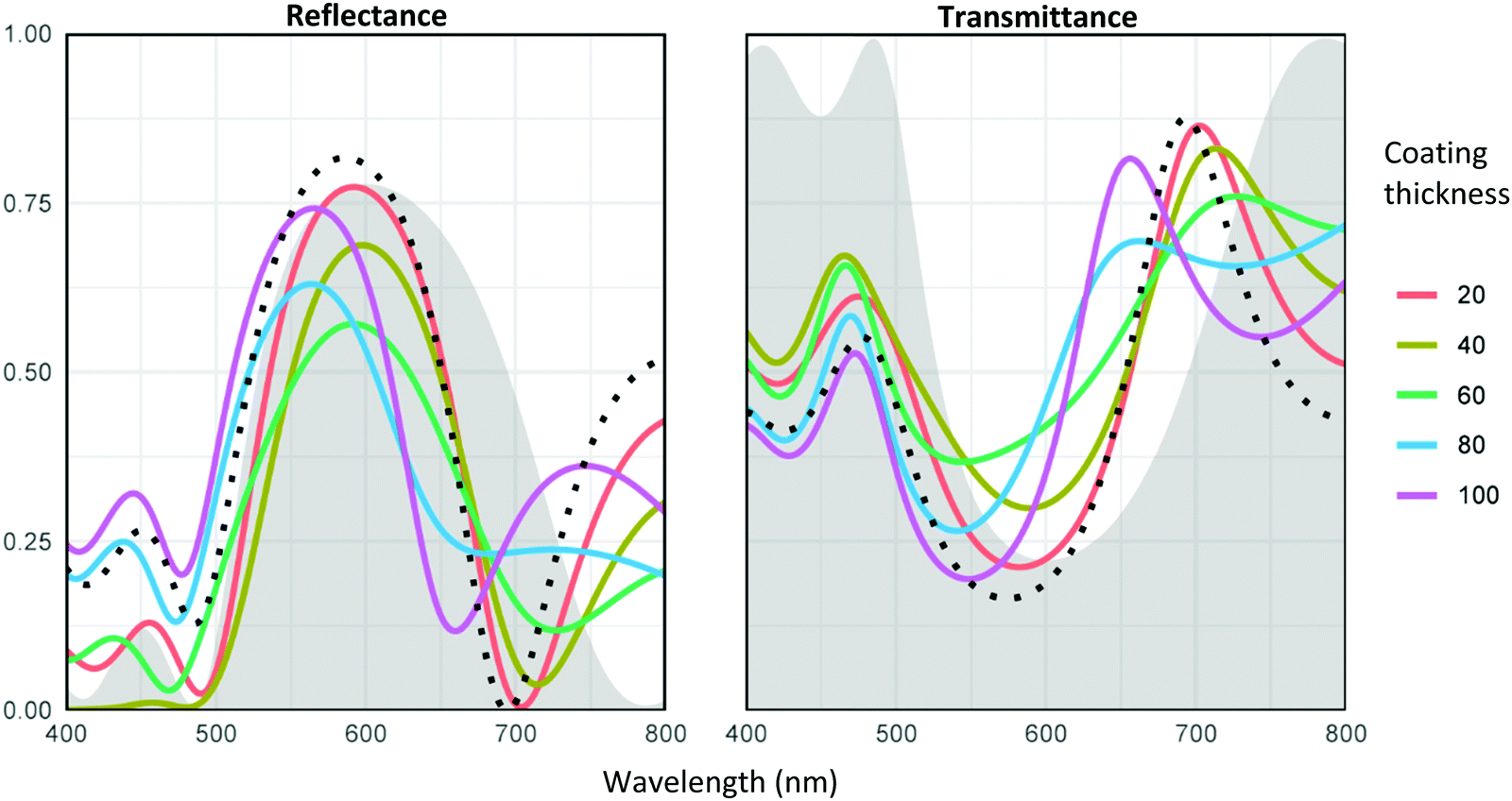 | ||
| Fig. 1 Variation of the reflectance (left) and the transmittance (right) spectra of a Tamm plasmon device with the incorporation of a superficial PL of different thicknesses from 20 to 100 nm. The grey shadows represent the corresponding DBR spectra (i.e. the device without the Au layer). The dotted black line corresponds to the bare TPP structure (no PL layer). | ||
The electric field of the TPP mode is confined around the metal/DBR interface,9,10 so the presence of an additional protective layer on top of Au is not expected to significantly alter the sensitivity of the TPP mode to changes of refractive index within the DBR; it may however affect the coupling of light to the structure. From the calculated spectra in Fig. 1 it is concluded that the PL should be kept thinner than about 40 nm in this structure. This small thickness is required to preserve a well-defined Tamm plasmon resonance: a sharp spectral feature despite a relatively small number of layers, associated with an enhanced electric field near the metal layer yielding a high sensitivity to changes of refractive index corresponding to the presence of analytes in this region.
In general, sol–gel film thickness can be controlled varying the solution composition and/or the deposition conditions.35,36 By changing the withdrawal speed for dip-coated films or the spin velocity for spin-coated films, the achievable range is limited and, in some cases, changes in sols composition are required to meet the target film thickness. In the present work, controlled amounts of ethanol were added to the sols; using this strategy, PLs with thickness between 20 and 30 nm were prepared on glass.
The second key feature to evaluate during the PL material selection is their capacity to protect the device from mechanical stress. Depending on the operating conditions, very hard/resistant or plastic/flexible PL could be required. Non-porous zirconia coatings have been used in several industries, owing to its mechanical, chemical and thermal stability.59,60 This material has also been widely used to protect metals due to its relatively high thermal expansion coefficient, good tribological features and excellent anticorrosion properties.61–65 Alternatively, inorganic–organic hybrid materials present the advantages of organic polymers, such as high fracture toughness, flexibility, resistance to impact, etc., combined with the properties of inorganic oxides: high mechanical strength and hardness.66
Following these considerations, three oxides were chosen to be tested as PLs:
(a) Porous zirconia (ZF), which has high thermal and chemical stability;67,68
(b) Porous titania–silica mixed oxide with phenyl groups inside the inorganic network and in the pores surface (TSP). The use of a mixed oxide has a double purpose: to have the mechanical and chemical properties of the titania matrix and to incorporate the organic species covalently-bonded to the silicon.66,69 The organic groups favor the enhancement of fracture toughness through the increase in dispersive interactions between the inorganic matrix and the organic group;70
(c) Porous titania–silica mixed oxide with vinyl groups inside the inorganic network and in the pores surface (TSV). This organic group provides the possibility to incorporate specific functions in the oxide through thiol–ene click reactions41,42,71 besides the improvement of the mechanical properties due to the presence of covalently-bonded organic groups.66,70
The material selection for PLs must also consider the capacity of this layer to allow analytes to reach the region of higher electric field within the DBR; thus, the chosen material should be porous to allow diffusion. The PLs synthetized in this work present an accessible porosity, obtained from XRR measurements, in the 15–30% range depending on the oxide (see Fig. S3 and more details in the ESI†). The mesopore array, determined from the SAXS measurements in transmission mode (Fig. S4, ESI†), is hexagonal p6mm for TSP72 and locally ordered derived from cubic Im3m phase for ZF and TSV.41,71 The interplanar distances in the direction parallel to the substrate calculated from the SAXS patters are (12.8 ± 0.5) nm for ZF (thermally treated at 300 °C), (14.5 ± 0.5) nm for TSP and (15.8 ± 0.5) nm for TSV (both treated up to 200 °C). These distances represent the addition of the pores diameters and the walls thicknesses, which are usually in the same range.73 Thus, a pore size of around 7 nm can be estimated for the three layers. These pore sizes, that are in agreement with previously measured ones for F127 templated oxides,24,73 are large enough not to limit the diffusion of the analytes by size, allowing their detection.74 Moreover, the structure contraction in the direction perpendicular to the substrate measured from the patterns is 50–55% for the hybrids and 72% for ZF. This dissimilarity is related with the applied thermal treatments: 200 °C were used for the hybrids while zirconia films were treated at 300 °C. This high contraction allows the interconnection of the pores, yielding the desired accessible mesoporosity.
3.2 Mechanical properties of the protective layer
The mechanical and tribological properties of the three PL candidates were evaluated before their application on top of the devices. 300–350 nm thick samples were obtained with 3 (ZF sample) or 2 (hybrids samples) successive layer depositions of the same oxide, as described in the experimental section. Nanoindentation studies were performed on these thick samples to obtain the oxides properties with almost no influence of the substrate (details can be found in ESI,† and Fig. S6).55,75Fig. 2 shows load vs. displacement curves and scratch patterns from which the mechanical and tribological features for each oxide were assessed. Additional measurements can be found in the ESI,† Fig. S5 and S7.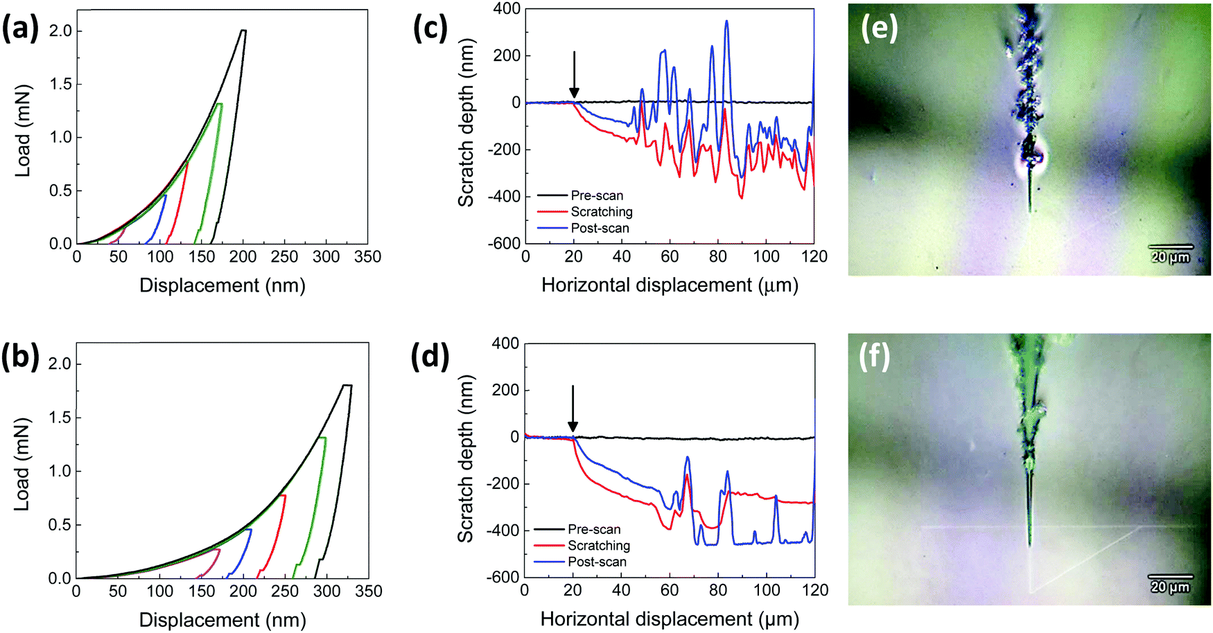 | ||
| Fig. 2 Selected load vs. displacement measurements (ISO method, maximum load of 2 mN) for ZF (a) and TSV (b). Examples of scratch measurements (c and d) and optical images (e and f) of the performed scratches for ZF (c and e) and for TSV (d and f), up to a maximum load of 5 mN. The arrows indicate the beginning of the scratching. | ||
Fig. 2a and b present selected load vs. displacement curves measured for ZF and TSV films, respectively. Each measurement was performed in a different region of the sample to avoid modification of the material due to multiple indentations in the same spot or densification/deformation effects due to a nearby indent.76,77 The hysteresis observed in the loading-unloading curves is ascribed to elastic-plastic behaviour, as the deformed region experiences only partial elastic recovery.55,78 The absence of pop-ins or discontinuities in all samples indicates that neither fracture nor delamination events are taking place in these nanoindentation experiments (see Fig. 2a, b and Fig. S5, ESI†).55 The porous structure is in part responsible for arresting cracks that could be generated during indentation in these systems. Moreover, the organic content in the case of the hybrid samples enhances the fracture toughness through a synergistic effect.70,79
E IT and HIT average values were calculated for the three oxides from the load vs. displacement measurements on Fig. 2 and Fig. S5, as detailed in the ESI.† The obtained values are shown in Table 1.
| PL | E IT (GPa) | H IT (GPa) | CL (mN) | D CL (nm) | D 0.5 (nm) | PD0.5 (%) |
|---|---|---|---|---|---|---|
| ZF | 45 ± 4 | 1.7 ± 0.1 | 1.0 ± 0.1 | 160 ± 10 | 116 ± 5 | 47 ± 5 |
| TSP | 9 ± 3 | 0.16 ± 0.03 | 1.2 ± 0.1 | 230 ± 20 | 190 ± 10 | 60 ± 10 |
| TSV | 9 ± 4 | 0.10 ± 0.03 | 1.7 ± 0.2 | 300 ± 30 | 200 ± 10 | 60 ± 10 |
For porous zirconia films, EIT is 5 times greater than the values obtained for the hybrids and HIT is over 10 times greater. Besides, both EIT and HIT are significantly lower than the reported values for dense zirconia films prepared using both sol–gel reactions65 or reactive magnetron sputtering.80 The differences in EIT and HIT values measured for the zirconia films in this work, compared to a fully dense material of similar composition, are essentially due to its porosity.81 For the titania-based hybrid films, EIT and HIT are slightly higher than the usual values obtained for silica-based hybrid oxides,66 mainly due to the mechanical properties of the titania matrix.69
Scratch test were performed also on the thick samples; these results are shown in Fig. 2c–f and Fig. S7 (ESI†) and the characteristic parameters obtained from the measurements are presented in Table 1. These tests usually provide semi quantitative information as there are several intrinsic (scratching speed, loading rate, tip radius, etc.) and extrinsic (substrate hardness, film thickness, film and substrate roughness, friction coefficient, etc.) parameters which may affect the film's performance during scratch.82 Nonetheless, this technique enables comparative measurements to rank the tribological behaviour of similar systems measured using the same experimental setup.55
The scratch resistance of coatings is usually expressed in terms of their ability to withstand abrasion without failure (fracture or delamination), and it is an important parameter to evaluate in the design of protective coatings resistant to handling. The failure mode mainly depends on the substrate and coating hardness.82 A scratch test usually involves a ramped load and the measure of performance is the critical load (CL), applied normal to the samples surface, at which the material fails.55 The CL value can be also associated with the adhesion strength between the substrate and the coating.83
The low roughness of these sol–gel synthesized samples is evidenced by the absence of noticeable discontinuities during the pre-scan curves: the measured arithmetic average roughness is less than 2 nm for the three oxides. In all the cases studied, a CL value was determined as a clear break in the scratching curve, just before the occurrence of a delamination or fracture event. ZF and TSP present lower CL values than TSV (1.0 and 1.2 mN vs. 1.7 mN), consistent with the more plastic character of this last hybrid film. The penetration depth at which the CL is detected (DCL) for TSV, and probably also for TSP, is related with the film/substrate interface, so it is possible that the failure mode for these hybrid oxides is delamination when the indenter tip is approaching the substrate. On the other hand, the DCL value found for ZF is about half of the thickness of this oxide; consequently, fracture is the most probable mode of failure in this case.
A load of 0.5 mN, that is half of the lower CL measured, was chosen to determine and compare the plastic behaviour of the candidates. The high HIT value obtained for ZF is compatible with the low penetration (D0.5) that is reached in this sample during the scratching, at the same load, compared to the hybrids. Also at this load, the percentage of plastic deformation (PD0.5) was calculated as the difference in depth between the post-scan curve and the pre-scan curves divided the difference between the scratching and the pre-scratch curves. This PD0.5 value represents a residual permanent deformation evidenced by the non-recovery of the initial surface topography. The obtained parameters (see Table 1) show that ZF films present a more elastic behaviour than the hybrids, as the amount of permanent deformation found for this oxide is lower at the same applied load. Finally, both values D0.5 and PD0.5 measured for TSP indicate that this sample present a ductile/plastic behaviour, similar to the one found for TSV.
From the observation of the optical images in Fig. 2 and Fig. S7 (ESI†), the correlation of the distance of failure from the beginning of the scratch with the CL values is noticeable. ZF presents less plastic deformation and breaks at lower loads, that is, at shorter distances from the beginning of the scratch compared with the other samples. In conclusion, the ZF layer is more brittle than the hybrid oxides, despite its greater HIT and EIT values.
3.3 Construction of protected Tamm plasmon devices and structural characterization
Following the mechanical characterization of the PLs, two systems were chosen to protect the TPP devices: ZF and TSV. ZF was selected due its very high hardness and its well-known chemical stability. Between the hybrids, which present a similar plastic behaviour, TSV was preferred due its reactivity, which allows the addition of several functions through the thiol–ene click reaction, as previously described.Three different TPP devices were built, one protected with ZF and two with TSV, with diverse structural and optical characteristics;9,24,48 the synthetic details can be found in the experimental section and the ESI.† The thicknesses of the layers that form each DBR were measured from cross-sectional SEM images. The Au layer thickness was obtained from the sputtering equipment's calibration. Thicknesses of the PL films deposited on top of the TPP devices were estimated from XRR measurements of single layers deposited onto glass. The detailed description of each protected TPP device prepared in this work can be found in Table 2.
| System | Silica layers thickness (nm) | Titania layers thickness (nm) | Au layer thickness (nm) | PL thickness (nm) |
|---|---|---|---|---|
| 4x(SC/TF)/Au/TSV | 70 ± 10 | 80 ± 10 | 20 ± 1 | 22 ± 2 |
| 4x(SC/TB)/Au/TSV | 75 ± 9 | 70 ± 20 | 20 ± 1 | 22 ± 2 |
| 4x(SB/TF)/Au/ZF | 40 ± 10 | 80 ± 10 | 20 ± 1 | 22 ± 3 |
In Fig. 3a, a cross-sectional SEM image is presented, which corresponds to a TPP device built with SC and TF films and a Au layer. It can be seen that the device is crack-free with no interpenetration between layers and each layer of the same oxide has a similar thickness, in accordance with previous results.9,47 Furthermore, the thin Au layer is present all over the multilayer. When the PL is deposited on top of the device, it homogeneously covers the Au layer with no significant cracks or flaws over the surface (see Fig. 4).
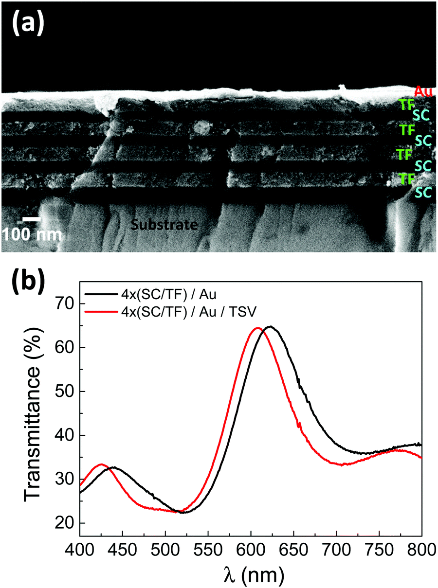 | ||
| Fig. 3 (a) Cross sectional SEM micrograph of 4x(SC/TF)/Au device. (b) Transmittance spectra of 4x(SC/TF)/Au and 4x(SC/TF)/Au/TSV devices, measured at 0% relative humidity. | ||
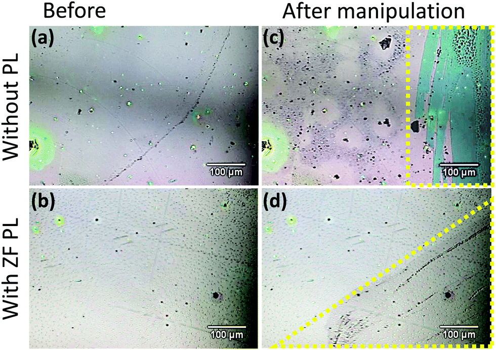 | ||
| Fig. 4 Optical microscopy photographs of the surface of Tamm plasmon devices with and without PL. 4x(SB/TF)/Au and 4x(SB/TF)/Au/ZF before (a and b) and after (c and d) macroscopic damage due to manipulation. The yellow dotted lines in (c and d) mark the areas that underwent simulated mechanical manipulation. | ||
The optical properties of the protected devices were compared with the unprotected sample: Fig. 3b shows the spectra of 4x(SC/TF)/Au with and without the TSV PL. Both devices present a well-defined Tamm mode, and it can be observed that the PL does not significantly affect the multilayer optical properties: the band preserves its width and intensity after the PL deposition, with an expected small change in peak position, as previously predicted by the simulations. The peak position is also influenced by minor differences in the DBR layers thicknesses between the spots measured on the protected and unprotected devices. The UV-visible spectra of the other protected devices presented in Table 2 are shown in Fig. S8 (4x(SB/TF)/Au/ZF) and S9 (4x(SC/TB)/Au/TSV), in the ESI.† These samples also present clear optical Tamm modes.
3.4 Mechanical integrity of the protected devices
The mechanical performance of the protected devices was tested and compared with that of the unprotected ones. Three types of studies were performed: determination of damage due to manipulation, observation of nanoindentation imprints at high penetrations and scratch tests to qualitatively evaluate plastic deformation and delamination of the devices.In Fig. 4, optical images of the same area of an uncoated device 4x(SB/TF)/Au are presented before (Fig. 4a) and after (Fig. 4c) scraping it with a cotton swab soaked in ethanol; this experiment was performed in order to simulate the manipulation of the device. The non-adherent behaviour of gold is observed: the stress made on the device completely removes the Au layer on top and blue-colored regions (marked with yellow dotted lines in Fig. 4c) appears due to the DBR light reflection.
On the other hand, Fig. 4b shows an equivalent device with a ZF PL. Although the same treatment was performed on this sample, the result is markedly different from that obtained for the unprotected one. The surface that suffered the mechanical test is not severely deteriorated, the protective layer remains well adhered and only a few small scratches can be observed (region delimited with yellow dotted lines in Fig. 4d), without changes in the optical properties of the device.
Nanoindentation imprints up to high penetration depth (1000 nm) were performed on 4x(SC/TB)/Au (Fig. 5a) and 4x(SC/TB)/Au/TSV (Fig. 5b) samples. The difference in the mechanical behaviour of the devices surface is clear: larger residual imprints can be seen due to the more pronounced permanent plastic deformation that suffers the unprotected TPP device compared with the protected one, under the same stress. Furthermore, it can be seen that in the case of the protected device, cracks are not propagating from the imprints significantly and there is no delamination of the layers forming the device.
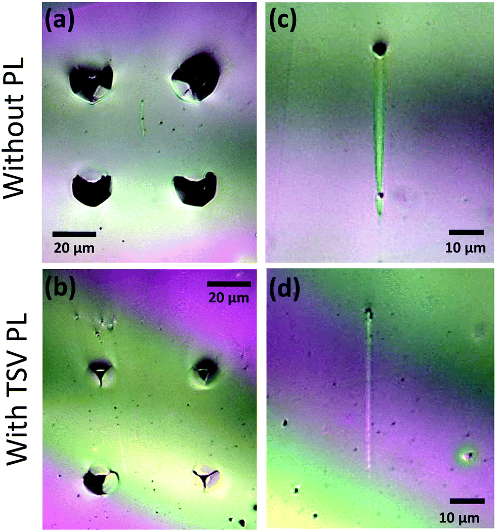 | ||
| Fig. 5 Optical microscopy photographs of the surface of Tamm plasmon devices with and without PL. Array of 4 indentations up to 1000 nm depth in 4x(SC/TB)/Au (a) and 4x(SC/TB)/Au/TSV (b); scratches in the same Tamm plasmon devices, without (c) and with (d) TSV PL. | ||
Similar results were found for these devices during scratch tests. The optical images show that the width of the residual scratch in the Au exposed device (2.5 to 3 μm, Fig. 5c) is about two times larger than the obtained for the protected device (1 to 1.5 μm, Fig. 5d), measured at half of the scratch length (25 μm). This observation implies that a greater plastic deformation is taking place in the unprotected device as the nanoindenter tip scratches the non-adherent Au layer, while a greater elastic recovery is presented by the TSV-protected device. In addition, there is no fracture or delamination of the PL also during this study, confirming the good adhesion of the hybrid oxide to the Au layer.
In conclusion, the selected PLs deposited on top of the Au layer effectively protect this layer from mechanical stress, avoiding the Au layer to be severely damaged or removed. The ZF PL supports the handling with no catastrophic failure, preserving the optical properties of the device, while the TSV PL minimizes the permanent deformation of the Au layer and provides a tough surface to the whole device. Moreover, hybrid oxides could be also applied to protect devices that have a poor mechanical performance or chemical stability, as some polymeric multilayered structures. In this case, the possibility to tune the protective layer wettability to improve the adhesion, opens new possibilities to integrate these ceramics films with plastic devices in order to build mechanically robust and chemically stable surfaces to interact with harsh environments.
3.5 Detection properties of the protected devices
Besides enhancing the mechanical strength, the addition of a PL should preserve the functionality of the device. The position of the Tamm plasmon resonance is very sensitive to small changes on the refractive index of the materials that build the DBR. Due to the particular pore size in the mesoscale, capillary condensation of vapours into the pores takes place at relatively low partial pressures (lower than the vapour pressure). Therefore, when exposed to solvent vapours the pores fill with solvent and the average refractive index of the porous material change, shifting the spectral peak position observed in transmission mode.TPP devices covered with TSV or ZF PL were evaluated as detectors of vapours and liquids. For these experiments, transmittance spectra of dry devices were recorded and compared with the spectra of the samples exposed to butanol. This solvent was chosen due to its high refractive index (n = 1.39658) which generates easily measurable shifts of the Tamm plasmon peak. Fig. 6a shows the response of 4x(SC/TF)/Au/TSV towards butanol vapours, presenting a maximum displacement of the Tamm plasmon peak (Δλmax) of around 20 nm. Moreover, when the device is exposed to the same solvent but in liquid phase it shows an equivalent optical response, confirming that exposure of the device to vapours completely fills the mesopores.24,48
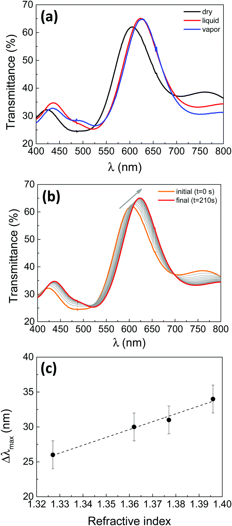 | ||
| Fig. 6 (a) UV-Visible spectra of 4x(SC/TF)/Au/TSV measured dry, in an atmosphere saturated with butanol vapour and after immersion in liquid butanol. (b) UV-visible spectra of the same device as a function of time in contact with liquid butanol. The orange curve corresponds to the initial state (dry, t = 0 s) and the red one to the final state (full of solvent, t = 210 s). (c) Linear calibration curve for the variation of the Tamm plasmon peak position of the protected device as a function of refractive index for different vapours (alcohols) filling the pores. | ||
Similar results were obtained for the other two protected Tamm detectors: 4x(SB/TF)/Au/ZF and 4x(SC/TB)/Au/TSV. Their response to solvent vapours is shown in Fig. S8 and S9 (ESI†), respectively. In these cases, the devices were exposed to water or butanol, and the results confirm that both PLs allow the entrance of these solvents to the multilayers. Crucially, the PL on top of the Au does not block the pathway to the analytes to the DBR-metal interface, allowing refractive index change detection with these protected devices.
As a further step, dynamic measurements were carried out in liquid butanol. Fig. 6b shows transmittance spectra for a 4x(SC/TF)/Au/TSV structure. A spectral evolution is observed, as the solvent diffuses and fills the pores of the DBR. Such changes are observed until all the accessible mesopores of the devices are filled with butanol (in this case, at a final time of 210 s) (see ESI,† Fig. S9b for dynamic results for 4x(SC/TB)/Au/TSV). The spectral shift of the Tamm plasmon mode and the time to complete the filling of the mesopore structure found for the studied systems are comparable to the previously reported values for unprotected TPP devices.24
Finally, the sensitivity of the devices was studied by exposing them to vapours of a series of alcohols with different refractive indexes (between 1.32 and 1.40). Fig. 6c present the changes in the Tamm plasmon mode position as a function of the alcohols bulk refractive index. It can be seen that this device presents the expected linear response to slight changes in medium refractive index,9 with a sensitivity of (112 ± 9) nm RIU−1. This behaviour is related with the penetration of the solvents into the device and the displacement of air (n = 1) from the pores, increasing the effective refractive index of each layer. Note that the composition, and therefore the refractive index, of each DBR layer is a mix of the solvent and the oxide matrix; consequently, the Tamm plasmon mode responds to a smaller refractive index change than that given by the bulk variation in alcohol refractive index.9,24 Similar results were obtained for 4x(SC/TB)/Au/TSV (Fig. S9c, ESI†). These results confirms that the presence of the PL does not affect significantly the device sensitivity towards the refractive index of the analytes, preserving the sensing capability of the devices.
4 Conclusions
An effective strategy to protect Tamm plasmon optical devices using sol–gel synthesized porous oxide thin films was proposed and demonstrated in this work. Firstly, by numerical simulation of the devices optical properties, it was shown that a thin (<40 nm) protective dielectric layer on top of the metallic film does not significantly deteriorate the optical response of Tamm plasmon based sensors. Accordingly, thin films of three different mesoporous materials were chosen and tested to act as protective layers: ZrO2 and Ti–Si mixed oxides functionalized with vinyl or phenyl groups. The mechanical and tribological properties of each candidate material were determined using nanoindentation, where it was found that ZrO2 presents an elastic and hard behaviour while Ti–Si hybrid films are plastic and tough.Two sets of protected devices were built and tested. Indentation, micro-scratching and manipulation were performed on the surface of the devices. The results confirm that thin mesoporous films provide a clear improvement in the device's resistance towards mechanical stress, alleviating removal of the metallic layer and minimizing the damage suffered by the device. Importantly, the presence of this protective layer does not significantly affect the optical and sensing properties of the system.
The effective and simple protection strategy based on a porous overlayer presented in this work can be extended to other devices which require interaction with the environment through an exposed surface. The accessible porosity of the proposed protective layer allows analytes to reach the sensitive region of the system while maintaining the mechanical integrity of the device. Moreover, the proposed approach could also be applied to protect other metal-terminated devices in which manipulation or interaction with the medium represents a risk for stability.
Conflicts of interest
There are no conflicts to declare.Acknowledgements
The authors acknowledge Elettra synchrotron and the CERIC-ERIC Consortium for access to experimental facilities and financial support (projects 20177003 and 20157040). This work was funded by Agencia Nacional de Promoción de la Investigación, el Desarrollo Tecnológico y la Innovación (PICT 2015-0351 and 2017-1133). The authors thank A. Fasciszewski and J. Bonaparte for the access to the clean room (CAC, CNEA), M. C. Marchi (CMA-FCEyN-UBA) for the FE-SEM images and G. Giménez for providing some reagents. JM and JIR acknowledge CONICET for their doctoral fellowships. MCF, PCA and AZ are CONICET researchers.References
- A. Bigdeli, F. Ghasemi, H. Golmohammadi, S. Abbasi-Moayed, M. A. F. Nejad, N. Fahimi-Kashani, S. Jafarinejad, M. Shahrajabian and M. R. Hormozi-Nezhad, Nanoscale, 2017, 9, 16546–16563 RSC.
- J. Homola, Chem. Rev., 2008, 108, 462–493 CrossRef CAS.
- H. Inan, M. Poyraz, F. Inci, M. A. Lifson, M. Baday, B. T. Cunningham and U. Demirci, Chem. Soc. Rev., 2017, 46, 366–388 RSC.
- H. Xu, P. Wu, C. Zhu, A. Elbaz and Z. Z. Gu, J. Mater. Chem. C, 2013, 1, 6087 RSC.
- F. Wang, Z. Meng, F. Xue, M. Xue, W. Lu, W. Chen, Q. Wang and Y. Wang, Trends Environ. Anal. Chem., 2014, 3, 1–6 Search PubMed.
- I. B. Burgess, M. Loncar and J. Aizenberg, J. Mater. Chem. C, 2013, 1, 6075–6086 RSC.
- H. Wang and K.-Q. Zhang, Sensors, 2013, 13, 4192 CrossRef CAS.
- C. Fenzl, T. Hirsch and O. S. Wolfbeis, Angew. Chem., Int. Ed., 2014, 53, 3318–3335 CrossRef CAS PubMed.
- B. Auguié, M. C. Fuertes, P. C. Angelomé, N. L. Abdala, G. J. A. A. Soler Illia and A. Fainstein, ACS Photonics, 2014, 1, 775–780 CrossRef.
- M. Kaliteevski, I. Iorsh, S. Brand, R. A. Abram, J. M. Chamberlain, A. V. Kavokin and I. A. Shelykh, Phys. Rev. B: Condens. Matter Mater. Phys., 2007, 76, 165415 CrossRef.
- Z. A. Zaky, A. M. Ahmed, A. S. Shalaby and A. H. Aly, Sci. Rep., 2020, 10, 9736 CrossRef CAS PubMed.
- S. Kumar, M. K. Shukla, P. S. Maji and R. Das, J. Phys. D: Appl. Phys., 2017, 50, 375106 CrossRef.
- G. Lheureux, M. Monavarian, R. Anderson, R. A. Decrescent, J. Bellessa, C. Symonds, J. A. Schuller, J. S. Speck, S. Nakamura and S. P. DenBaars, Opt. Express, 2020, 28, 17934–17943 CrossRef CAS PubMed.
- W. L. Zhang, F. Wang, Y. J. Rao and Y. Jiang, Opt. Express, 2014, 22, 14524–14529 CrossRef CAS PubMed.
- L. Qin, S. Wu, C. Zhang and X. Li, IEEE Sens. J., 2019, 19, 2924–2930 CAS.
- X. Zhang, X. Zhu and Y. Shi, IEEE Sens. J., 2019, 19, 2570–2575 CAS.
- X. Zhang, X. S. Zhu and Y. W. Shi, Sensors, 2018, 18(7), 2129 CrossRef PubMed.
- A. M. Ahmed and A. Mehaney, Sci. Rep., 2019, 9, 6973 CrossRef PubMed.
- S. Kumar and R. Das, J. Appl. Phys., 2018, 123, 233103 CrossRef.
- N. Li, T. Tang, J. Li, L. Luo, P. Sun and J. Yao, Sens. Actuators, B, 2018, 265, 644–651 CrossRef CAS.
- P. S. Maji, M. K. Shukla and R. Das, Sens. Actuators, B, 2018, 255, 729–734 CrossRef CAS.
- M. Mehdi Keshavarz and A. Alighanbari, Appl. Opt., 2020, 59, 4517–4526 CrossRef CAS PubMed.
- B. Du, Y. Li, D. Yang and H. Lu, Appl. Opt., 2019, 58, 4569–4574 CrossRef CAS.
- M. C. Sansierra, J. Morrone, F. Cornacchiulo, M. C. Fuertes and P. C. Angelomé, ChemNanoMat, 2019, 5, 1289–1295 CrossRef CAS.
- Y. Tsurimaki, J. K. Tong, V. N. Boriskin, A. Semenov, M. I. Ayzatsky, Y. P. Machekhin, G. Chen and S. V. Boriskina, ACS Photonics, 2018, 5, 929–938 CrossRef CAS.
- F. Sohrabi, S. M. Hamidi, N. Asgari, M. A. Ansari and R. Gachiloo, Opt. Mater., 2019, 96, 109275 CrossRef CAS.
- M. Todeschini, A. Bastos da Silva Fanta, F. Jensen, J. B. Wagner and A. Han, ACS Appl. Mater. Interfaces, 2017, 9, 37374–37385 CrossRef CAS PubMed.
- S. Yamazaki, in Handbook of Sol–Gel Science and Technology, ed. L. Klein, M. Aparicio and A. Jitianu, Springer International Publishing, Cham, 2017, DOI:10.1007/978-3-319-19454-7_97-1, pp. 1–16.
- H. E. Çamurlu, Ö. Kesmez, E. Burunkaya, N. Kiraz, Z. Yeşil, M. Asiltürk and E. Arpaç, Chemical Papers, 2012, 66, 461–471 Search PubMed.
- V. A. Ganesh, H. K. Raut, A. S. Nair and S. Ramakrishna, J. Mater. Chem., 2011, 21, 16304–16322 RSC.
- P. Nguyen-Tri, H. N. Tran, C. O. Plamondon, L. Tuduri, D.-V. N. Vo, S. Nanda, A. Mishra, H.-P. Chao and A. K. Bajpai, Prog. Org. Coat., 2019, 132, 235–256 CrossRef CAS.
- I. R. Durán and G. Laroche, Prog. Mater. Sci., 2019, 99, 106–186 CrossRef.
- H. K. Raut, V. A. Ganesh, A. S. Nair and S. Ramakrishna, Energy Environ. Sci., 2011, 4, 3779–3804 RSC.
- T. Zada, M. Reches and D. Mandler, J. Sol-Gel Sci. Technol., 2020, 95, 609–619 CrossRef CAS.
- L. C. Huang, E. K. Richman, B. L. Kirsch and S. H. Tolbert, Microporous Mesoporous Mater., 2006, 96, 341–349 CrossRef CAS.
- D. Grosso, J. Mater. Chem., 2011, 21, 17033–17038 RSC.
- M. Faustini, C. Boissiere, L. Nicole and D. Grosso, Chem. Mater., 2014, 26, 709–723 CrossRef CAS.
- A. Fischer, M. Kuemmel, M. Järn, M. Linden, C. Boissière, L. Nicole, C. Sanchez and D. Grosso, Small, 2006, 2, 569–574 CrossRef.
- M. Kuemmel, C. Boissière, L. Nicole, C. Laberty-Robert, C. Sanchez and D. Grosso, J. Sol-Gel Sci. Technol., 2008, 48, 102–112 CrossRef CAS.
- C. Sanchez, C. Boissière, D. Grosso, C. Laberty and L. Nicole, Chem. Mater., 2008, 20, 682–737 CrossRef CAS.
- A. Escobar, N. E. Muzzio, Á. M. Martínez-Villacorta, A. Abarrategi, E. Bindini, M. Grzelczak, A. V. Bordoni, P. C. Angelomé and S. E. Moya, Appl. Surf. Sci., 2020, 510, 145172 CrossRef CAS.
- A. Bordoni, M. V. Lombardo and A. Wolosiuk, RSC Adv., 2016, 6, 77410–77426 RSC.
- C. J. Brinker, Y. Lu, A. Sellinger and H. Fan, Adv. Mater., 1999, 11, 6 CrossRef.
- G. J. A. A. Soler-Illia, P. C. Angelomé and P. Bozzano, Chem. Commun., 2004, 2854 RSC.
- E. L. Crepaldi, G. J. A. A. Soler-Illia, D. Grosso, F. Cagnol, F. Ribot and C. Sanchez, J. Am. Chem. Soc., 2003, 125, 9770–9786 CrossRef CAS PubMed.
- P. C. Angelomé, M. C. Fuertes and G. J. A. A. Soler-Illia, Adv. Mater., 2006, 18, 2397–2402 CrossRef.
- M. C. Fuertes, F. J. López-Alcaraz, M. C. Marchi, H. E. Troiani, V. Luca, H. Míguez and G. J. A. A. Soler-Illia, Adv. Funct. Mater., 2007, 17, 1247–1254 CrossRef CAS.
- M. C. Fuertes, S. Colodrero, G. Lozano, A. R. González-Elipe, D. Grosso, C. Boissière, C. Sánchez, G. J. A. A. Soler-Illia and H. Míguez, J. Phys. Chem. C, 2008, 112, 3157–3163 CrossRef CAS.
- B. Auguié, A. Bruchhausen and A. Fainstein, J. Optics, 2015, 17, 035003 CrossRef.
- Z. Knittl, Optics of Thin Films: An Optical Multilayer Theory, Wiley, London, 1976 Search PubMed.
- P. B. Johnson and R. W. Christy, Phys. Rev. B: Condens. Matter Mater. Phys., 1972, 6, 4370–4379 CrossRef CAS.
- H. Amenitsch, S. Bernstorff, M. Kriechbaum, D. Lombardo, H. Mio, M. Rappolt and P. Laggner, J. Appl. Crystallogr., 1997, 30, 872–876 CrossRef CAS.
- A. van der Lee, Solid State Sci., 2000, 2, 257–278 CrossRef CAS.
- P. Y. Steinberg, M. M. Zalduendo, G. Giménez, G. J. A. A. Soler-Illia and P. C. Angelomé, Phys. Chem. Chem. Phys., 2019, 21, 10347–10356 RSC.
- A. C. Fischer-Cripps, Nanoindentation, Springer, Third Edition, 2011 Search PubMed.
- D. Mercier, A. Nicolay, A. Boudiba, X. Vanden Eynde, L. Libralesso, A. Daniel and M. Olivier, J. Sol-Gel Sci. Technol., 2020, 93, 229–243 CrossRef CAS.
- J. Malzbender, J. M. J. den Toonder, A. R. Balkenende and G. de With, Mater. Sci. Eng., R, 2002, 36, 47–103 CrossRef.
- D. R. Lide, CRC Handbook of Chemistry and Physics, 84th edn, 2003 Search PubMed.
- C. Piconi and G. Maccauro, Biomaterials, 1999, 20, 1–25 CrossRef CAS.
- M. Catauro, F. Bollino, F. Papale, R. Giovanardi and P. Veronesi, Mater. Sci. Eng., C, 2014, 43, 375–382 CrossRef CAS PubMed.
- K. Izumi, M. Murakami, T. Deguchi, A. Morita, N. Tohge and T. Minami, J. Am. Ceram. Soc., 1989, 72, 1465–1468 CrossRef CAS.
- M. Atik and M. A. Aegerter, J. Non-Cryst. Solids, 1992, 147–148, 813–819 CrossRef CAS.
- M. Guglielmi, J. Sol-Gel Sci. Technol., 1997, 8, 443–449 CAS.
- D. Wang and G. P. Bierwagen, Prog. Org. Coat., 2009, 64, 327–338 CrossRef CAS.
- Y. Chen and W. Liu, J. Am. Ceram. Soc., 2002, 85, 2367–2369 CrossRef CAS.
- F. Mammeri, E. L. Bourhis, L. Rozes and C. Sanchez, J. Mater. Chem., 2005, 15, 3787–3811 RSC.
- E. L. Crepaldi, G. J. d. A. A. Soler-Illia, D. Grosso and C. Sanchez, New J. Chem., 2003, 27, 9–13 RSC.
- A. Zelcer and G. J. A. A. Soler-Illia, J. Mater. Chem. C, 2013, 1, 1359–1367 RSC.
- D. F. Lionello, P. Y. Steinberg, M. M. Zalduendo, G. J. A. A. Soler-Illia, P. C. Angelomé and M. C. Fuertes, J. Phys. Chem. C, 2017, 121, 22576–22586 CrossRef CAS.
- K. Vanstreels, M. Krishtab, L. G. Gonzalez and S. Armini, Appl. Phys. Lett., 2017, 111, 161906 CrossRef.
- A. Escobar, L. Yate, M. Grzelczak, H. Amenitsch, S. E. Moya, A. V. Bordoni and P. C. Angelomé, ACS Omega, 2017, 2, 4548–4555 CrossRef CAS PubMed.
- M. Klotz, P.-A. Albouy, A. Ayral, C. Ménager, D. Grosso, A. Van der Lee, V. Cabuil, F. Babonneau and C. Guizard, Chem. Mater., 2000, 12, 1721–1728 CrossRef CAS.
- G. J. A. A. Soler-Illia, P. C. Angelome, M. C. Fuertes, D. Grosso and C. Boissiere, Nanoscale, 2012, 4, 2549–2566 RSC.
- J. F. Angiolini, M. Stortz, P. Y. Steinberg, E. Mocskos, L. Bruno, G. Soler-Illia, P. C. Angelomé, A. Wolosiuk and V. Levi, Phys. Chem. Chem. Phys., 2017, 19, 26540–26544 RSC.
- S. Chen, L. Liu and T. Wang, Surf. Coat. Technol., 2005, 191, 25–32 CrossRef CAS.
- A. C. Fischer-Cripps, J. Mater. Res., 2007, 22, 3075–3086 CrossRef CAS.
- G. Carè and A. C. Fischer-Cripps, J. Mater. Sci., 1997, 32, 5653–5659 CrossRef.
- I. Pana, C. Vitelaru, A. Kiss, N. C. Zoita, M. Dinu and M. Braic, Mater. Des., 2017, 130, 275–284 CrossRef CAS.
- B. A. Latella, B. K. Gan, C. J. Barbé and D. J. Cassidy, J. Mater. Res., 2008, 23, 2357–2365 CrossRef CAS.
- H. Zegtouf, N. Saoula, M. Azibi, L. Bait, N. Madaoui, M. R. Khelladi and M. Kechouane, Surf. Coat. Technol., 2020, 393, 125821 CrossRef CAS.
- K. Vanstreels, C. Wu, P. Verdonck and M. R. Baklanov, Appl. Phys. Lett., 2012, 101, 123109 CrossRef.
- S. J. Bull and E. G. Berasetegui, Tribol. Int., 2006, 39, 99–114 CrossRef CAS.
- M. H. Blees, G. B. Winkelman, A. R. Balkenende and J. M. J. den Toonder, Thin Solid Films, 2000, 359, 1–13 CrossRef CAS.
Footnotes |
| † Electronic supplementary information (ESI) available. See DOI: 10.1039/d1ma00079a |
| ‡ J. M. and J. I. R. contributed equally to this work. |
| This journal is © The Royal Society of Chemistry 2021 |