
 Open Access Article
 This Open Access Article is licensed under a Creative Commons Attribution-Non Commercial 3.0 Unported Licence
Zero-dimensional plate-shaped copper halide crystals with green-yellow emissions†
Feng
Liu
 a,
Debayan
Mondal
b,
Kai
Zhang
c,
Ying
Zhang
a,
Keke
Huang
a,
Dayang
Wang
a,
Wensheng
Yang
a,
Priya
Mahadevan
*b and
Renguo
Xie
*a
a,
Debayan
Mondal
b,
Kai
Zhang
c,
Ying
Zhang
a,
Keke
Huang
a,
Dayang
Wang
a,
Wensheng
Yang
a,
Priya
Mahadevan
*b and
Renguo
Xie
*a
aState Key Laboratory of Inorganic Synthesis and Preparative Chemistry, College of Chemistry Jilin University, Changchun 130012, China. E-mail: renguoxie@jlu.edu.cn
bDepartment of Condensed Matter Physics and Material Science, S.N. Bose National Centre for Basic Sciences, Kolkata 700106, India. E-mail: priya@bose.res.in
cState Key Laboratory of Structural Chemistry, Fujian Institute of Research on the Structure of Matter, Chinese Academy of Sciences, Fuzhou, Fujian 350002, China
First published on 8th April 2021
Abstract
Low-cost and eco-friendly metal hybrid materials with zero-dimensional (0D) structures have recently attracted increasing attention owing to their excellent optical properties and wide applications. However, successful examples of 0D structural OIMHs with well-defined dimensions are still quite limited. Here, plate-shaped copper-based halide hybrids, (DTA)2Cu2I4, with 0D structures were successfully prepared by the employment of long alkyl chain molecules. The crystallization features were characterized by X-ray diffraction, and further investigated by theoretical simulations. The investigation on the photophysical properties indicates that 0D crystals show a broadband emission peak at ∼540 nm with a high PLQY of 60%, a long lifetime of 1.84 μs and a large Stokes shift of 210 nm under photo-excitation. The broad emission should be attributed to the self-trapping excitons as determined by the joint experiment-density functional theory studies. Also, the high optical performance and stability endow (DTA)2Cu2I4 with the potential for lighting phosphors by fabricating a white light-emitting diode (WLED) device. Importantly, bright PL at the edge of the plate-shaped crystal was observed, suggesting a typical waveguide behavior in a 2D system. These results validate these 2D crystals as promising luminescent materials for potential optical communication micro-devices.
Introduction
Luminescent organic–inorganic metal hybrids (OIMHs) have attracted tremendous attention due to their excellent optoelectronic properties coupled with potential applications in photovoltaics,1–4 light-emitting diodes5–8 and lasers.9,10 Generally, the optical properties of OIMHs are totally dominated by the crystal structure dimensions, i.e., inherent molecular structures.11–14 For instance, lowering the dimensionality from three-dimensional (3D) to 2D, 1D or 0D leads excitons to be confined in the confined inorganic blocks and consequently facilitates the self-trapping of excitons, giving rise to self-trapped excitons (STEs). As a result, the broadband photoluminescence (PL) with large Stokes shifts, near-unity PL quantum efficiencies, zero self-absorption and longer lifetimes is usually observed in these 0D OIMH compounds.15–20 On the other hand, the optical properties of OIMH compounds also rely on the external morphology such as size, shapes and dimensions. For example, 1D/2D and/or micro-/nano-sized crystals such as wires, rods and belts have shown unique optical characteristics for polarized emissions and optical waveguides. To date, research on OIMH compounds has mainly focused on the preparation of crystals with different inherent molecular structures. By comparison, very few studies have been carried out on the control of the external morphology of OIMH compounds, probably because of the lack of a suitable synthesis approach.Cu-based emitters, as a representative of luminescent materials, have been widely reported due to their inexpensive green metal center, excellent optical properties, earth abundance and nontoxicity.21 In the past decade, the vast majority of copper hybrid materials reported have been coordination complexes whose structural stability is relatively poor.22–24 By contrast, recently, Cu-based 0D OIMH compounds have been reported by the formation of an ionic complex in copper hybrid materials, instead of a coordination complex,25 which exhibit high PL quantum yields (PLQYs) and excellent stability.26,27 Unfortunately, much effort has been mainly devoted to fabricating bulk OIMH compounds, and no study has been carried out on the control of their external morphologies.
After careful analysis of the 0D crystal structure, an obvious fact is that the crystal structure is entirely dominated by the assembly of crystal unit cells consisting of organic shells and a metal halide core. It would be feasible to control the dimensions of these 0D crystals by tuning the shell molecular configuration. It has been shown in our recent studies that the morphology of Sb-based OIMHs is tunable by the employment of organic cations with long carbon chains. Based on this fact, the design and synthesis of copper-based OIMHs with different morphologies should be feasible by the employment of special organic molecules during crystallization.
Herein, we report a copper-based OIMH, (DTA)2Cu2I4, with a 2D plate-shaped morphology, in which isolated tetraiodide ions (Cu2I4) are surrounded by organic cations (DTA)+ to form a 0D structure. The micro-plates exhibit a broadband emission peak at about 540 nm, with a PLQY of 60%, and a large Stokes shift of 210 nm. Photophysical studies indicate that the luminescence of (DTA)2Cu2I4 should be ascribed to the radiative recombination of STEs. Importantly, a bright PL at the edge of the plate-shaped crystal was observed, which suggests a typical characteristic of waveguide behavior in a 2D system. Thus, the current work provides a facile way to develop 0D OIMM-based low-dimensional photonic strategies.
Results and discussion
(DTA)2Cu2I4 micro-plate crystals were synthesized through a simple one-step anti-solvent precipitation approach. Typically, CuI and DTAI (DTAI![[thin space (1/6-em)]](https://www.rsc.org/images/entities/char_2009.gif) :CuI = 1:1, 0.083 M in acetone) were dissolved in acetone solution and then 200 μL of the obtained precursor solution was quickly added dropwise into toluene (8.0 mL) under vigorous stirring at room temperature. The transparent solution immediately becomes turbid with white suspended solids exhibiting a bright yellow luminescence under UV-302 nm irradiation, suggesting the formation of new products as shown in Fig. 1a. The as-prepared samples have a plate-shaped morphology with a size of 30 × 8 μm2 (length × width), determined from the optical microscopy photograph shown in Fig. 1b. The cross-sectional scanning electron microscopy (SEM) image shows that the sample has a thickness of 1.2 μm as shown in Fig. S2 (ESI†). Energy-dispersive X-ray spectrometry (EDXS) mappings in Fig. 1c indicate that Cu and I elements are unambiguously distributed in the whole micro-plates, suggesting the uniform element distributions along the micro-plates. The atomic ratio of Cu/I is determined to be close to 1:1 in Fig. S3 (ESI†). Note that when the obtained precursor solution with different concentrations was used, instead of 0.083 M, the samples still show plate-shaped products with a size of 200 × 25 μm2 to 80 × 3.5 μm2 as shown in Fig. S1 (ESI†), suggesting that the size of the micro-plates is tunable by simply controlling the precursor concentrations. The SEM test was performed on two samples with different reaction concentrations (Fig. S4, ESI†). The micro-plate morphology of these samples with different length–width ratios can be clearly observed. At low concentrations, they are more similar to micro-ribbons with a polygon cross-section rather than micro-rods. With the increase of the concentration, the length–width ratio of the sample decreases gradually. The morphology of the (DTA)2Cu2I4 crystal is affected by the arrangement of organic molecules. This fact is consistent with the fact that the morphologies of crystals are mainly dependent on the molecular structures.28 The morphology of the (DTA)2Cu2I4 crystal is affected by the arrangement of organic molecules which is similar to the crystallization of organic crystals.
:CuI = 1:1, 0.083 M in acetone) were dissolved in acetone solution and then 200 μL of the obtained precursor solution was quickly added dropwise into toluene (8.0 mL) under vigorous stirring at room temperature. The transparent solution immediately becomes turbid with white suspended solids exhibiting a bright yellow luminescence under UV-302 nm irradiation, suggesting the formation of new products as shown in Fig. 1a. The as-prepared samples have a plate-shaped morphology with a size of 30 × 8 μm2 (length × width), determined from the optical microscopy photograph shown in Fig. 1b. The cross-sectional scanning electron microscopy (SEM) image shows that the sample has a thickness of 1.2 μm as shown in Fig. S2 (ESI†). Energy-dispersive X-ray spectrometry (EDXS) mappings in Fig. 1c indicate that Cu and I elements are unambiguously distributed in the whole micro-plates, suggesting the uniform element distributions along the micro-plates. The atomic ratio of Cu/I is determined to be close to 1:1 in Fig. S3 (ESI†). Note that when the obtained precursor solution with different concentrations was used, instead of 0.083 M, the samples still show plate-shaped products with a size of 200 × 25 μm2 to 80 × 3.5 μm2 as shown in Fig. S1 (ESI†), suggesting that the size of the micro-plates is tunable by simply controlling the precursor concentrations. The SEM test was performed on two samples with different reaction concentrations (Fig. S4, ESI†). The micro-plate morphology of these samples with different length–width ratios can be clearly observed. At low concentrations, they are more similar to micro-ribbons with a polygon cross-section rather than micro-rods. With the increase of the concentration, the length–width ratio of the sample decreases gradually. The morphology of the (DTA)2Cu2I4 crystal is affected by the arrangement of organic molecules. This fact is consistent with the fact that the morphologies of crystals are mainly dependent on the molecular structures.28 The morphology of the (DTA)2Cu2I4 crystal is affected by the arrangement of organic molecules which is similar to the crystallization of organic crystals.
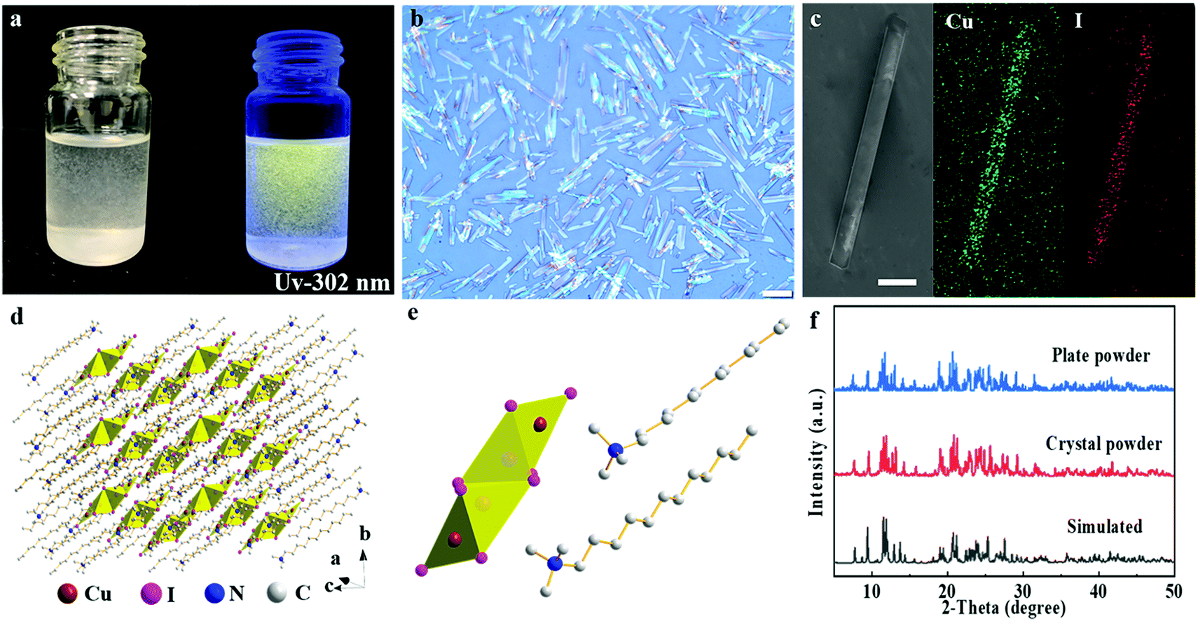 | ||
| Fig. 1 (a) The photograph of (DTA)2Cu2I4 micro-plate crystals in toluene under light/UV-302 nm. (b) Optical microscopy photograph of the as-prepared micro-plate crystals. (c) SEM-EDS elemental mapping image of the selected micro-plate crystal (scale bars are 20 μm). The green color is from the Cu element, and the red color is from the I element crystal (scale bars are 10 μm). (d) Single crystal structure diagram of (DTA)2Cu2I4 (pink spheres: iodine atom; brown spheres: copper atom; dark blue spheres: nitrogen atoms; gray spheres: carbon atoms; yellow polyhedral, [Cu4I8] tetranuclear halogenocuprates; hydrogen atoms are hidden for the sake of clarity). (e) Side view of the individual [Cu4I8] and two adjacent (DTA)+ cations. (f) The Powder X-ray diffraction pattern of single crystal/micro-pate crystal powders as well as simulation results. | ||
To characterize the crystal structures of the samples, the plate-like crystals with sizes on the order of millimeters were prepared as shown in Fig. S5 (ESI†). The crystal structure of (DTA)2Cu2I4 was determined by single-crystal X-ray diffraction (SXRD) analysis. The product adopts a triclinic space group P![[1 with combining macron]](https://www.rsc.org/images/entities/char_0031_0304.gif) with the individual tetranuclear halogenocuprates [Cu4I8]4− surrounded by large organic ligands, DTA− cations, to form a 0D structure at the molecular level (Fig. 1d). Detailed single-crystal diffraction data are summarized in Tables S1–S3 (ESI†). This [Cu4I8]4− presenting a linear arrangement and two crystallographic independent Cu atoms has two kinds of coordination modes (CuI3 and CuI4) (Fig. 1e). The nearest distance between the two [Cu4I8]4− was close to 1 nm (8.8 Å), leading to an ignorable intermolecular coupling between [Cu4I8]4− anions. Therefore, (DTA)2Cu2I4 forms a real 0D structure at the molecular level,14 which is different from those copper-based hybrid materials built on a coordinate. As a result, the 0D copper-based crystals show excellent thermal stability, even if saturated at 230 °C as verified by thermogravimetric analysis (TGA), shown in Fig. S6 (ESI†). The measured powder X-ray diffraction (PXRD) patterns of the micro-plate/single crystals are in accordance with the calculated single-crystal data, confirming the reliability of the SXRD results.
with the individual tetranuclear halogenocuprates [Cu4I8]4− surrounded by large organic ligands, DTA− cations, to form a 0D structure at the molecular level (Fig. 1d). Detailed single-crystal diffraction data are summarized in Tables S1–S3 (ESI†). This [Cu4I8]4− presenting a linear arrangement and two crystallographic independent Cu atoms has two kinds of coordination modes (CuI3 and CuI4) (Fig. 1e). The nearest distance between the two [Cu4I8]4− was close to 1 nm (8.8 Å), leading to an ignorable intermolecular coupling between [Cu4I8]4− anions. Therefore, (DTA)2Cu2I4 forms a real 0D structure at the molecular level,14 which is different from those copper-based hybrid materials built on a coordinate. As a result, the 0D copper-based crystals show excellent thermal stability, even if saturated at 230 °C as verified by thermogravimetric analysis (TGA), shown in Fig. S6 (ESI†). The measured powder X-ray diffraction (PXRD) patterns of the micro-plate/single crystals are in accordance with the calculated single-crystal data, confirming the reliability of the SXRD results.
The structural characterization of 2D plate-shaped (DTA)2Cu2I4 crystals was further revealed by small-angle XRD patterns of a plate-like single crystal and micro-plates shown in Fig. 2a. The small-angle XRD patterns of the crystal without grinding could show its self-assembly structural properties. Obviously, the single crystal/plate-shaped crystals presented a perfect layered structural feature of an intense Bragg reflection and the upper surfaces of the crystals are attributed to the (001) plane (Fig. 2a). The thickness of the layer was calculated to be 22.83 Å according to the XRD measurement results, which is identical to the distance of adjacent organic molecular layers in the crystal structure (Fig. 2b). Generally, OIMHs with 3D morphology were observed for the organic molecules with the same short chain length (alkyl carbon atoms: N(Ca)4, a = 1–4).25,29 Thus, the formation of 2D plate-shaped crystals is completely dominated by the molecular configuration due to the employment of DTAI with a long alkyl chain (C12), which results in anisotropic growth or assembly induced by van der Waals forces. To gain further insight into the growth mechanism of plate-shaped crystals, theoretical simulations of the crystal morphology were carried out using Materials Studio software.30 According to the calculation results, the (001) face has larger attachment energy than other crystal faces, showing that the growth tendency on the (001) face is weaker (Table S4, ESI†). The simulation results demonstrate the 2D growth trend of single plate-like crystals and micro-plates controlled by their layered non-covalent interaction characteristics. It can be seen from the high-magnification SEM image (Fig. S7, ESI†) that the morphology of the crystal with typical lattice planes is in good agreement with the simulation results.
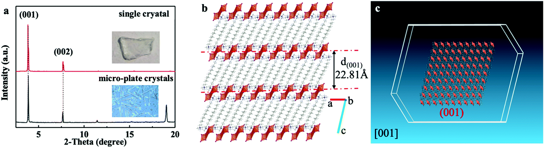 | ||
| Fig. 2 (a) The X-ray diffraction pattern of single crystal and micro-plate crystals. (b) Layered packing structures of the (DTA)2Cu2I4 crystal. (c) The predicted growth morphology of the (DTA)2Cu2I4 crystal. | ||
To gain insight into the electronic properties of (DTA)2Cu2I4, we have calculated the electronic structure and density of states (DOS) using a plane-wave projector-augmented wave implementation of density functional theory (DFT) in the software package VASP. We used the generalised gradient form PBE for the exchange–correlation functional. Fig. 3a shows the results of the density functional theory (DFT) calculations, which unravel the presence of direct bandgaps of 2.75 eV between the valence and conduction bands at Γ points in the electronic structures of (DTA)2Cu2I4. Built on the UV-vis diffuse reflectance spectra of the as-prepared micro-rods, the Tauc plots indicate that the (direct) bandgap of the crystals is 3.52 eV (Fig. S8, ESI†). As is well known, the DFT calculations generally underestimate the bandgaps.31,32 The valence band and conduction band of (DTA)2Cu2I4 are nearly flat, indicating the strong confinement effect for 0D OIMHs.33 As shown in Fig. 3b, the projected density of states (DOS) of the crystals shows that the valence band of (DTA)2Cu2I4 is contributed by Cu 3d and I 5p states, while the conduction band is contributed by Cu 4s states. Fig. 2c and d show that the charge densities of the valence band maximum (VBM) and conduction band minimum (CBM) are mainly distributed within the inorganic Cu–I clusters, respectively, indicating a zero electronic dimensionality and can explain the high quantum yields found in experiments. The calculation result is consistent with the intrinsic structure where two adjacent [Cu4I8]4− are completely isolated by large organic molecules (DTA+), which results in the occurrence of emission in the inorganic [Cu4I8]4− unit as a separate luminescence center (see below).
 | ||
| Fig. 3 (a) Band dispersions along symmetry directions and the (b) Cu s, Cu d and I p contributions to the density of states in (DTA)2Cu2I4. (c) The charge density corresponding to the VBM and CBM. The inset of panel (c) also shows the localization of the CBM charge density. | ||
The plate-shaped (DTA)2Cu2I4 crystals display bright yellow-green luminescence under UV irradiation (302 nm; Fig. 4a), which inspired us to study the photophysical properties of the 0D copper-based hybrids. Fig. 4a shows the excitation and emission spectra; the emission spectrum is mainly dominated by a broad emission band with a PL peak at 533 nm, and the peak of the PL excitation spectrum (PLE) is at 320 nm. The absorption spectra in Fig. S6 (ESI†) exhibit a sharp absorption peak at 330 nm below the band edge, indicating that the PLE at 320 nm originates from the excitonic absorption of (DTA)2Cu2I4. The quantum yield was estimated to be about 60% as shown in Fig. S9 (ESI†). These results, including a large Stokes shift of about 210 nm, high quantum yield, and broad emission band with a full width at half-maximum of 180 nm, suggest that the emission is similar to those of 0D hybrid materials.34,35 The peak position and the shape of the excitation/emission spectra at different wavelengths are almost similar, indicating that the emission comes from the same excited state,15 which further rules out the possibility of defect-related emissions. To understand the photophysical properties, a time-resolved PL experiment was conducted at room temperature. As shown in Fig. 4b, a long single exponential lifetime of 1.84 μs is observed, which is much similar to that of 0D copper-iodide materials.36,37 Such a prolonged lifetime at room temperature combined with a large Stokes shift and excitation/emission spectra (Fig. 4a) indicates that the broadband emission is due to a single phosphorescence process arising from the spin-forbidden transition rather than multiple radiation mechanisms.38
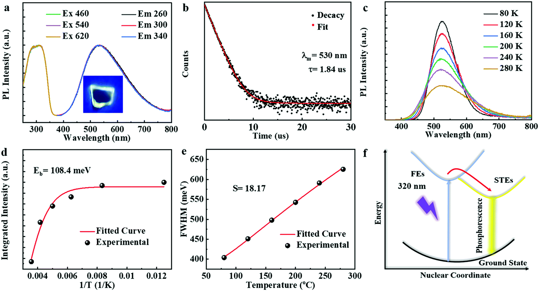 | ||
| Fig. 4 (a) Excitation and emission spectra of (DTA)2Cu2I4 at different wavelengths (inset: the photograph of plate-shaped (DTA)2Cu2I4 single crystals under UV-302 nm). (b) The PL decay curve of (DTA)2Cu2I4 (monitored at 530 nm) excited at 320 nm. (c) Temperature-dependent photoluminescence spectra of (DTA)2Cu2I4. (d) Fitting results of the FWHM as a function of temperature. (e) Integrated PL intensity as a function of reciprocal temperature from 80 to 280 K for (DTA)2Cu2I4. (f) Schematic diagram of the photophysical processes in (DTA)2Cu2I4. | ||
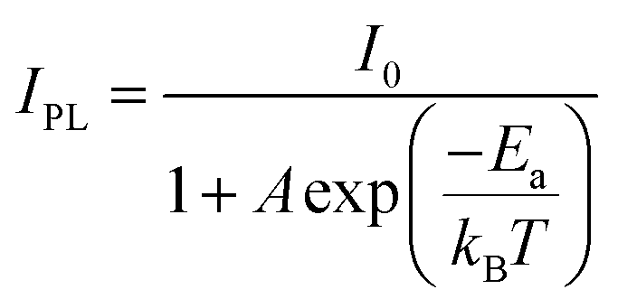
To further probe the intrinsic nature of the PL, the temperature-dependent luminescence properties of (DTA)2Cu2I4 were investigated. Fig. 4c shows the PL spectra in the temperature range of 80–280 K. Only one broadband emission is observed, indicating that the self-trapping barrier is low and the excitons are easily trapped.38 The FWHM broadens significantly, and simultaneously, the PL intensity increases monotonously with the decreasing temperature, both of which suggest that the broad emission does not originate from multiple radiative mechanisms.39–41Fig. 4d shows the plots of the temperature-dependent integrated PL intensity. The exciton binding energy (Ea) can be derived from the following Arrhenius eqn (1):
 | (1) |
 | (2) |
Because of its good thermal stability and high PLQY, (DTA)2Cu2I4 could be potentially useful as a white-light-emitting phosphor. Hence, we have prepared a two-component copper-based phosphor by a simple ball grinding method. By introducing (DTA)2Cu2I4 (yellow-green light) in the Cs3Cu2I5 (blue light) composition process, phosphors with different light under UV-302 nm were successfully prepared as shown in Fig. 5a. Fig. 4b shows the luminescence spectrum of those phosphors excited at 310 nm. The CIE color coordinates corresponding to those phosphors from (0.16, 0.13) to (0.34, 0.44) are marked in Fig. 4c. The phosphor (1:2.8) was used to prepare phosphor-converting white-light-emitting diodes (WLEDs) with a commercial LED (310 nm) as the excitation source. The working device exhibits a bright white light with a high CRI of 85.7. Excellent stability was observed in this phosphor when exposed to 302 nm UV irradiation (6 W), as shown in Fig. S10 (ESI†). After 6 hours, the intensity of the phosphor can be maintained at 97%. Also, the intensity of the device can be maintained at 80% after the system had been run at 20 mA for 400 min (Fig. S11, ESI†).
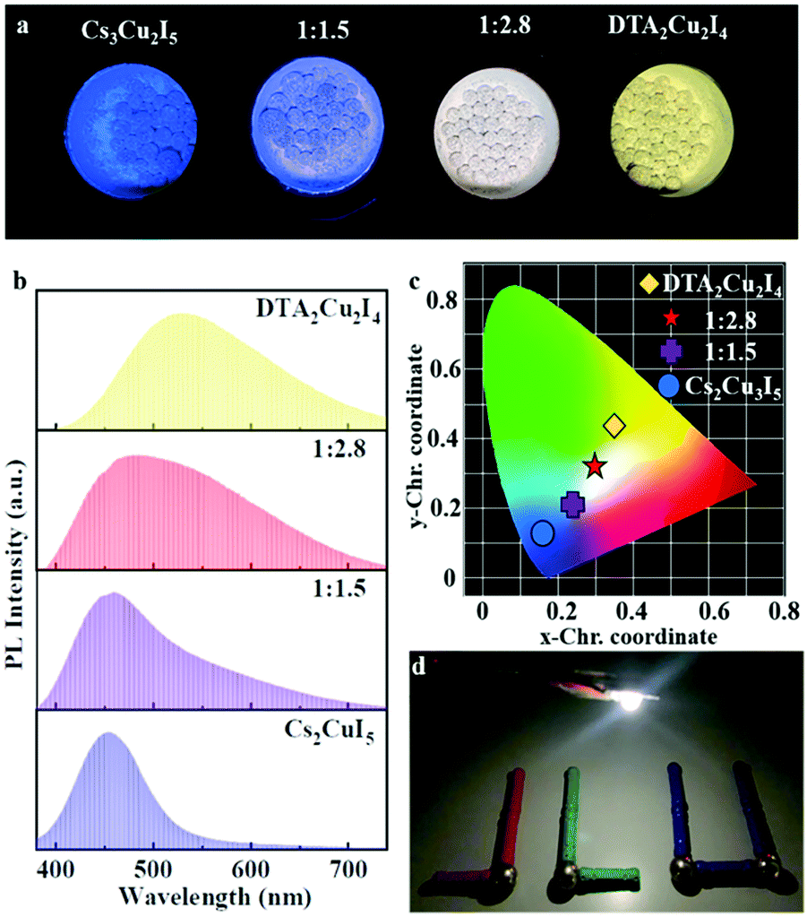 | ||
| Fig. 5 (a) Photographs of ball grinding powders of the composites of Cs3Cu2I5 and (DTA)2Cu2I4 prepared with different molar ratios under UV-302 mm. (b) PL spectra of the powder samples. (c) CIE color coordinates of the powder samples. (d) A typical photograph of the working device with a high CRI of 85.7 prepared with the powder samples in the molar ratios of 1:2.8. | ||
Significantly, a notably bright PL at the edge of the plate-shaped crystals was observed, whereas the surface showed no visualized emissions (Fig. 4a inset and Fig. S12, ESI†). This phenomenon revealed that the 2D plate-shaped crystals could transport the PL emission toward the edge of the crystal under light excitation. Such localization of the out-coupling light at the edge of each crystal was a typical characteristic of waveguide behaviour. These results imply that the current work provides a facile way to develop 0D OIMH-based low-dimensional photonic systems and their potential application in photo-communication.
Conclusions
In conclusion, we have successfully synthesized a novel lead-free, plate-shaped (DTA)2Cu2I4 single crystal with a 0D structure by the wet chemical method. The formation of plate-shaped crystals is totally dominated by the chain length of organic molecules as confirmed by theoretical simulations. As expected, a highly luminescent green-yellow emission, with a large Stokes shift of 210 nm and a high PLQY of around 60%, was observed for the plate-shaped crystals. Experimental and computational studies reveal that the intrinsic PL nature of the plate-shaped crystals originates from STEs. Also, the high optical performance and stability endow (DTA)2Cu2I4 with the potential for lighting phosphors by fabricating a white-light-emitting diode (WLED) device. Importantly, the phenomenon of optical waveguides was observed for the plate-shaped crystals, indicating that 0D OIHMs are promising materials for the construction of future optical communication and photo-functional micro-devices.Experimental section
Materials and preparation
:CuI = 1:1, 0.1667/0.0833/0.0083 M in acetone). 200 μL of the precursor solution was quickly added dropwise into 8 mL of toluene under vigorous stirring at room temperature. The transparent solution immediately becomes turbid with a white suspended matter suggesting the formation of micro-plate crystals.
:1.5 1:2.8). Then, ball milling was performed with a QM-3SP04 Planetary ball mill from Nanda, at a frequency of 35 Hz for 240 min.
:2.8 were mixed with silicone and deposited on the UV LED chip.
Characterization methods
A single crystal was mounted on a thin glass fiber and transferred into the cold nitrogen stream of a Bruker APEX-II CCD diffractometer. X-ray powder diffraction patterns were obtained using a Philips PW1830 X-ray diffractometer. The diffraction patterns were scanned with a step size of 0.026 at room temperature. Thermogravimetric analysis (TGA) was carried out with a TA Discovery TGA550 (TA Instruments) equipped with a continuous nitrogen flow. Measurements were performed with a ramp of 10 °C min−1 from room temperature to 800 °C. UV-vis spectra were recorded using a Shimadzu U-4100 spectrophotometer. The excitation and emission spectra of the samples were obtained using an Edinburgh FLS920 spectrophotometer. PL lifetime decays were acquired using FLS920 steady-state fluorescence spectrometers. The lifetime was obtained by single-exponential fitting. Temperature-dependent emission and decay data were collected using an FLS9820 spectrophotometer equipped with a closed-cycle cryostat. The PLQYs were determined using an integrating sphere (150 mm in diameter, BaSO4 coating) from the FLS920 fluorescence spectrophotometer.DFT method
All calculations were performed by projector-augmented wave (PAW) implementation of density functional theory within the Vienna Ab initio Simulation Package (VASP).53,54 The generalized gradient approximation (GGA) was used for the exchange-correlation functional.55 Inclusion of the nonlocal, weak van der Waals (vdW) interactions is necessary to correctly predict the structural properties. GGA+vdW density functional theory calculations have been found to give a good estimation of the lattice parameters. The DFT-D2 method of Grimme was considered to introduce dispersive interactions within the system.56 A gamma-point k-point mesh was used for initial relaxations, while a gamma-centred 4 × 4 × 2 k-point mesh was used for the calculation of the density of states. In addition, an energy cutoff of 400 eV was used for the kinetic energy of the plane waves included in the basis. The lattice parameters and the internal positions were optimized until the forces on the atoms were less than 10−3 eV Å−1 to find the minimum energy structure. The density of states has been broadened by a Gaussian of 0.1 eV full width at half maximum.Conflicts of interest
There are no conflicts to declare.Acknowledgements
This work was supported by the National Natural Science Foundation of China (21373097 and 51872114) and the National Basic Research Program of China (21932003).Notes and references
- Z. Li, T. R. Klein, D. H. Kim, M. Yang, J. J. Berry, M. F. A. M. Van Hest and K. Zhu, Nat. Rev. Mater., 2018, 3, 18017–18036 CrossRef CAS.
- J. P. Correa-Baena, M. Saliba, T. Buonassisi, M. Graetzel, A. Abate, W. Tress and A. Hagfeldt, Science, 2017, 358, 739–744 CrossRef CAS PubMed.
- S. Shao, J. Liu, G. Portale, H. H. Fang, G. R. Blake, G. H. Ten Brink, L. J. A. Koster and M. A. Loi, Adv. Energy Mater., 2018, 8, 1702019 CrossRef.
- D. Prochowicz, R. Runjhun, M. M. Tavakoli, P. Yadav, M. Saski, A. Q. Alanazi, D. J. Kubicki, Z. Kaszkur, S. M. Zakeeruddin and J. Lewiński, Chem. Mater., 2019, 31, 1620–1627 CrossRef CAS.
- K. Lin, J. Xing, L. N. Quan, F. P. G. de Arquer, X. Gong, J. Lu, L. Xie, W. Zhao, D. Zhang, C. Yan, W. Li, X. Liu, Y. Lu, J. Kirman, E. H. Sargent, Q. Xiong and Z. Wei, Nature, 2018, 562, 245–248 CrossRef CAS PubMed.
- X. Yang, X. Zhang, J. Deng, Z. Chu, Q. Jiang, J. Meng, P. Wang, L. Zhang, Z. Yin and J. You, Nat. Commun., 2018, 9, 570–577 CrossRef PubMed.
- H. Cho, J. S. Kim, C. Wolf, Y. H. Kim, H. J. Yun, S. H. Jeong, A. Sadhanala, V. Venugopalan, J. W. Choi and C. L. Lee, ACS Nano, 2018, 12, 2883–2892 CrossRef CAS PubMed.
- H. Tsai, W. Nie, J. C. Blancon, C. C. Stoumpos, C. M. M. Soe, J. Yoo, J. Crochet, S. Tretiak, J. Even, A. Sadhanala, G. Azzellino, R. Brenes, P. M. Ajayan, V. Bulovic, S. D. Stranks, R. H. Friend, M. G. Kanatzidis and A. D. Mohite, Adv. Mater., 2018, 30, 1704217 CrossRef PubMed.
- H. Zhang, Q. Liao, Y. Wu, Z. Zhang and H. Fu, Adv. Mater., 2018, 30, 1706186 CrossRef PubMed.
- H. Zhu, Y. Fu, F. Meng, X. Wu, Z. Gong, Q. Ding, M. V. Gustafsson, M. T. Trinh, S. Jin and X. Y. Zhu, Nat. Mater., 2015, 14, 636–642 CrossRef CAS PubMed.
- H. Lin, C. Zhou, Y. Tian, T. Siegrist and B. Ma, ACS Energy Lett., 2018, 3, 54–62 CrossRef CAS.
- L. Mao, Y. Wu, C. C. Stoumpos, M. R. Wasielewski and M. G. Kanatzidis, J. Am. Chem. Soc., 2017, 139, 5210–5215 CrossRef CAS PubMed.
- A. Biswas, R. Bakthavatsalam, S. R. Shaikh, A. Shinde, A. Lohar, S. Jena, R. G. Gonnade and J. Kundu, Chem. Mater., 2019, 31, 2253–2257 CrossRef CAS.
- C. Zhou, H. Lin, H. Shi, Y. Tian, C. Pak, M. Shatruk, Y. Zhou, P. Djurovich, M. H. Du and B. Ma, Angew. Chem., Int. Ed., 2018, 57, 1021–1024 CrossRef CAS PubMed.
- M. D. Smith and H. I. Karunadasa, Acc. Chem. Res., 2018, 51, 619–627 CrossRef CAS PubMed.
- L. Mao, Y. Wu, C. C. Stoumpos, B. Traore and M. G. Kanatzidis, J. Am. Chem. Soc., 2017, 139, 11956–11963 CrossRef CAS PubMed.
- C. Zhou, H. Lin, Y. Tian, Z. Yuan and B. Ma, Chem. Sci., 2018, 9, 586–593 RSC.
- C. Zhang, Y. Yan, Y. S. Zhao and J. Yao, Acc. Chem. Res., 2014, 47, 3448–3458 CrossRef CAS PubMed.
- E. R. Dohner, E. T. Hoke and H. I. Karunadasa, J. Am. Chem. Soc., 2014, 136, 1718–1721 CrossRef CAS PubMed.
- E. R. Dohner, A. Jaffe, L. R. Bradshaw and H. I. Karunadasa, J. Am. Chem. Soc., 2014, 136, 13154–13157 CrossRef CAS PubMed.
- W. Liu, Y. Fang and J. Li, Adv. Funct. Mater., 2018, 28, 13154–13157 Search PubMed.
- J. J. Shen, X. X. Li, T. L. Yu, F. Wang, P. F. Hao and Y. L. Fu, Inorg. Chem., 2016, 55, 8271–8273 CrossRef CAS PubMed.
- M. M. Xu, Y. Li, L. J. Zheng, Y. Niu and H. Hou, New J. Chem., 2016, 40, 6086–6092 RSC.
- W. Liu, Y. Fang, G. Z. Wei, S. J. Teat, K. C. Xiong, Z. C. Hu, W. P. Lustig and J. Li, J. Am. Chem. Soc., 2015, 137, 9400–9408 CrossRef CAS PubMed.
- S. Chen, J. Gao, J. Chang, Y. Li, C. Huangfu, H. Meng, Y. Wang, G. Xia and L. Feng, ACS Appl. Mater. Interfaces, 2019, 11, 17513–17520 CrossRef CAS PubMed.
- Y. Fang, W. Liu, S. J. Teat, G. Dey, Z. Shen, L. An, D. Yu, L. Wang, D. M. O'Carroll and J. Li, Adv. Funct. Mater., 2017, 27, 1603444 CrossRef.
- S. Wang, E. E. Morgan, P. Vishnoi, L. Mao, S. M. L. Teicher, G. Wu, Q. Liu, A. K. Cheetham and R. Seshadri, Inorg. Chem., 2020, 59, 15487–15494 CrossRef CAS PubMed.
- Q. Q. Zhou, Y. L. Lei and H. B. Fu, J. Mater. Chem. C, 2021, 9, 489–496 RSC.
- Z. Li, Y. Li, P. Liang, T. Zhou and R. J. Xie, Chem. Mater., 2019, 31, 9363–9371 CrossRef CAS.
- D. Winn and M. F. Doherty, AIChE J., 2000, 46, 1348–1367 CrossRef CAS.
- D. Chen, S. Hao, G. Zhou, C. Deng, Q. Liu, S. Ma, C. Wolverton, J. Zhao and Z. Xia, Inorg. Chem., 2019, 58, 15602–15609 CrossRef CAS PubMed.
- H. Peng, S. Yao, Y. Guo, R. Zhi, X. Wang, F. Ge, Y. Tian, J. Wang and B. Zou, J. Phys. Chem. Lett., 2020, 11, 4703–4710 CrossRef CAS PubMed.
- G. Song, M. Li, S. Zhang, N. Wang, P. Gong, Z. Xia and Z. Lin, Adv. Funct. Mater., 2020, 30, 2002468 CrossRef CAS.
- C. Zhou, M. Worku, J. Neu, H. Lin, Y. Tian, S. Lee, Y. Zhou, D. Han, S. Chen and A. Hao, Chem. Mater., 2018, 30, 2374–2378 CrossRef CAS.
- X. Zhang, Z. Chi, Y. Zhang, S. Liu and J. Xu, J. Mater. Chem. C, 2013, 1, 3376–3390 RSC.
- L. Lian, M. Zheng, P. Zhang, Z. Zheng and J. Zhang, Chem. Mater., 2020, 32, 3462–3468 CrossRef CAS.
- S. Li, J. Xu, Z. Li, Z. Zeng and Y. Du, Chem. Mater., 2020, 32, 6525–6531 CrossRef CAS.
- X. Liu, W. Wu, Y. Zhang, Y. Li and J. Fan, J. Phys. Chem. Lett., 2019, 10, 7586–7593 CrossRef CAS PubMed.
- S. Li, J. Luo, J. Liu and J. Tang, J. Phys. Chem. Lett., 2019, 10, 1999–2007 CrossRef CAS PubMed.
- Z. Tan, J. Li, C. Zhang, Z. Li, Q. Hu, Z. Xiao, T. Kamiya, H. Hosono, G. Niu, E. Lifshitz, Y. Cheng and J. Tang, Adv. Funct. Mater., 2018, 28, 1801131 CrossRef.
- T. Hu, M. D. Smith, E. R. Dohner, M. J. Sher, X. Wu, M. T. Trinh, A. Fisher, J. Corbett, X. Y. Zhu, H. I. Karunadasa and A. M. Lindenberg, J. Phys. Chem. Lett., 2016, 7, 2258–2263 CrossRef CAS PubMed.
- C. Y. Yue, C. Sun, D. Y. Li, Y. H. Dong and X. W. Lei, Inorg. Chem., 2019, 58(15), 10304–10312 CrossRef CAS PubMed.
- L. Zhou, J. F. Liao, Z. G. Huang, J. H. Wei, X. D. Wang, H. Y. Chen and D. B. Kuang, Angew. Chem., Int. Ed., 2019, 58, 15435–15440 CrossRef CAS PubMed.
- H. Yang, Y. Zhang, J. Pan, J. Yin, O. M. Bakr and O. F. Mohammed, Chem. Mater., 2017, 29, 8978–8982 CrossRef CAS.
- W. Stadler, D. M. Hofmann, H. C. Alt, T. Muschik, B. K. Meyer, E. Weigel, G. Müller-Vogt, M. Salk, E. Rupp and K. W. Benz, Phys. Rev. B: Condens. Matter Mater. Phys., 1995, 51, 10619–10628 CrossRef CAS PubMed.
- V. Türck, S. Rodt, O. Stier, R. Heitz, R. Engelhardt, U. W. Pohl, D. Bimberg and R. Steingrüber, Phys. Rev. B: Condens. Matter Mater. Phys., 2000, 61, 9944–9947 CrossRef.
- H. Zhao and H. Kalt, Phys. Rev. B: Condens. Matter Mater. Phys., 2003, 68, 125309 CrossRef.
- X. Lao, Z. Yang, Z. Su, Z. Wang, H. Ye, M. Wang, X. Yao and S. Xu, Nanoscale, 2018, 10, 9949–9956 RSC.
- J. Luo, X. Wang, S. Li, J. Liu, Y. Guo, G. Niu, L. Yao, Y. Fu, L. Gao and Q. Dong, Nature, 2018, 563, 541–545 CrossRef CAS PubMed.
- L. Zhou, J. F. Liao, Z. G. Huang, J. H. Wei, X. D. Wang, W. G. Li, H. Y. Chen, D. B. Kuang and C. Y. Su, Angew. Chem., Int. Ed., 2019, 58, 5277–5281 CrossRef CAS PubMed.
- K. S. Song and R. T. Williams, Self-trapped excitons, Springer Berlin Heidelberg, 1993 Search PubMed.
- S. L. Paz, N. A. Javier, S. Michele, P. Francisco and H. J. Bolink, Chem. Mater., 2019, 31, 10205–10210 CrossRef.
- G. Kresse and J. Furthmuller, Phys. Rev. B: Condens. Matter Mater. Phys., 1996, 54, 11169–11186 CrossRef CAS PubMed.
- P. E. Blochl, Phys. Rev. B: Condens. Matter Mater. Phys., 1994, 50, 17953–17979 CrossRef PubMed.
- J. P. Perdew, K. Burke and M. Ernzerhof, Phys. Rev. Lett., 1996, 77, 3865–3868 CrossRef CAS PubMed.
- S. Grimme, Wiley Interdiscip. Rev.: Comput. Mol. Sci., 2011, 1, 211–228 CAS.
Footnote |
| † Electronic supplementary information (ESI) available: Details of additional synthetic, structural, and thermal properties and extended photophysical data. CCDC 2054832. For ESI and crystallographic data in CIF or other electronic format see DOI: 10.1039/d1ma00061f |
| This journal is © The Royal Society of Chemistry 2021 |