
 Open Access Article
 This Open Access Article is licensed under a
 Creative Commons Attribution 3.0 Unported Licence
Pulsed chemical vapor deposition of conformal GeSe for application as an OTS selector†
Ali
Haider
a,
Shaoren
Deng
b,
Wouter
Devulder
a,
Jan Willem
Maes
b,
Jean-Marc
Girard
c,
Gabriel
Khalil El Hajjam
a,
Gouri Sankar
Kar
a,
Karl
Opsomer
ad,
Christophe
Detavernier
ad,
Michael
Givens
b,
Ludovic
Goux
a,
Sven
Van Elshocht
a,
Romain
Delhougne
a,
Annelies
Delabie
ae,
Matty
Caymax
*a and
Johan
Swerts
a
aIMEC, Belgium. E-mail: matty.caymax@imec.be
bASM-Belgium, Belgium
cAir Liquide, France
dTU Ghent, Belgium
eKU Leuven, Belgium
First published on 8th January 2021
Abstract
The ovonic threshold switch (OTS) selector based on the voltage snapback of amorphous chalcogenides has received tremendous attention as it provides several desirable characteristics such as bidirectional switching, a controllable threshold voltage, high drive currents, and low leakage currents. GeSe is a well-known OTS selector that fulfills all the requirements imposed by future high-density storage class memories. Here, we report on pulsed chemical vapor deposition (CVD) of amorphous GeSe by using GeCl2·C4H8O2 as a Ge source and two different Se sources namely bis-trimethylsilylselenide ((CH3)3Si)2Se (TMS)2Se and bis-triethylsilylselenide ((C2H5)3Si)2Se (TES)2Se. We utilized total reflection X-ray fluorescence (TXRF) to study the kinetics of precursor adsorption on the Si substrate. GeCl2·C4H8O2 precursor adsorption on a 300 mm Si substrate showed under-dosing due to limited precursor supply. On the other hand, the Se precursor adsorption is limited by low reaction efficiency as we learned from a better within-wafer uniformity. Se precursors need Cl sites (from Ge precursor) for precursor ligand exchange reactions. Adsorption of (TMS)2Se is found to be much faster than (TES)2Se on a precoated GeClx layer. Atomic layer deposition (ALD) tests with GeCl2·C4H8O2 and (TMS)2Se revealed that the growth per cycle (GPC) decreases with the introduction of purge steps in the ALD cycle, whereas a higher GPC is obtained in pulsed-CVD mode without purges. Based on this basic understanding of the process, we developed a pulsed CVD growth recipe (GPC = 0.3 Å per cycle) of GeSe using GeCl2·C4H8O2 and (TMS)2Se at a reactor temperature of 70 °C. The 20 nm GeSe layer is amorphous and stoichiometric with traces of chlorine and carbon impurities. The film has a roughness of ∼0.3 nm and it starts to crystallize at a temperature of ∼370 °C. GeSe grown on 3D test structures showed excellent film conformality.
Introduction
Computer memory can be broadly categorized into two segments: volatile memory and non-volatile memory (NVM).1 Volatile memory requires power to maintain the stored information and its typical examples are static random-access memory (SRAM) and dynamic RAM (DRAM). Major advantages of volatile memory include high speed and fast access. On the other hand, the access to NVM is relatively slower but it can retain the stored information even when powered-off and it is therefore considered as long-term persistent storage. Typical NVM examples are magnetic storage devices (hard disks) and NAND flash. The storage density, cost, and performance gap between DRAM and NAND can be fulfilled by a new non-volatile memory (NVM) candidate: resistive random-access memory (RRAM).1 RRAM – an emerging type of memory based on resistive switching is regarded as a promising technology for next-generation embedded and standalone NVM.2 RRAM promises near-DRAM performance, but with lower cost and higher density.The typical RRAM configuration is the so-called cross-point array, which includes bit lines, word lines, and memory cells located at the intersection of each bit and word line. Ideally, writing or reading a memory cell in a cross-point array is meant to take place only on the selected cell, leaving the rest of the cells unaffected. However, current sneaks through unselected cells during operation, degrading the selectivity of the cell and leading to false information retrieval.3 An attractive approach is to have an additional selection device called a selector in series with each memory element that suppresses sneak currents through highly nonlinear current–voltage (IV) characteristics. Ovonic threshold switching (OTS) selector devices have received much attention as they provide full cell selectivity, high drive currents, and low leakage currents.3 The concept of the OTS mechanism refers to a rapid and reversible transition between a highly resistive and a conductive state effected by an electric field.4 The 3D RRAM approach, which combines the advantages of excellent electrical performance in RRAM cells and an ultra-high storage density with low cost due to the 3D configuration, becomes a very attractive candidate for next generation high density NVM applications. A 3D integration route for RRAM involves multiple selector–resistor stacks in sequence, without requiring litho steps in between. To fabricate this innovative 3D vertical RRAM, a main challenge remains – the uniform and conformal deposition of the chalcogenide selector material on 3D substrates.
Recent studies have shown that PVD grown GeSe is one of the most promising candidates for OTS selector devices owing to its high amorphous stability, large on/off current ratio, high selectivity, and large driving current.5–8 Note that this amorphous stability is critical since threshold OTS switching is a characteristic of the amorphous phase and no crystallization is involved for the material to function as a selector. Amorphous stability can be enhanced by addition of ternary and quaternary elements in binary germanium chalcogenide materials that impede easy crystallization; for example, it has been demonstrated that PVD-grown N-doped GeSe,9 SiGeTe10 and SiAsGeTe11 showed better OTS switching characteristics with enhanced amorphous stability. Nevertheless, the adopted PVD method with its limited step coverage cannot be used for conformal deposition on 3D memory structures. Atomic layer deposition (ALD) stands out as a material deposition technique that enables the conformal growth of thin films with sub-angstrom thickness control and excellent large-area uniformity.12–14 Chemical vapor deposition can also provide excellent conformality if suitable process conditions are utilized. For example, it has been shown that favourable combination of precursors with high partial pressure, low temperature reactivity and fast diffusivity can bring decent conformality in CVD-grown films.15,16
ALD of GeTe, Sb2Te3, and GeSbTe has been demonstrated at low growth temperatures (60–90 °C) using alkylsilylchalcogenide ((i.e. (R3Si)2Te)) and metal chloride (i.e. GeCl2·dioxane) precursors.17,18 This is a hard–soft acid base chemistry wherein (R3Si)2Te a hard Lewis acid (i.e. Si) is bonded to the heavy group 16 elements, which are soft Lewis bases, thus forming an unfavourable hard–soft Lewis acid–base pair. Upon exchange reaction with metal chlorides, for example, Si becomes bonded to the harder base providing enough driving force to complete the reaction:
| (R3Si)2Te + MCl2 → MTe + 2R3SiCl |
This dehalosilylation chemistry appears to be very powerful to grow chalcogenide materials in an amorphous state at low deposition temperatures.17,18 ALD of GeTe2 or GeTe films has also been demonstrated using other Ge precursors such as Ge(OEt)4,19 HGeCl3,20 and Ge{N[Si(CH3)3]2}2.21 Alkoxy-Ge precursors in combination with alkylsilylchalcogenide precursors have been used to grow GeSbTe films as well.22,23 However, alkoxy-Ge precursors’ non-ideal physisorption (lack of strong chemical adsorption) and the high oxidation state (+4) limit their use in the deposition of stoichiometric GeSe. Recently, ALD of amorphous GeSe has been demonstrated using HGeCl3 and [(CH3)3Si]2Se as Ge and Se precursors, respectively.24 HGeCl3 has a very high vapor pressure (30 torr at 3 °C) and it easily decomposes in the precursor cannister into HCl and GeCl2. This instability combined with the very high vapor pressure make HGeCl3 less favourable for GeSe growth in high volume manufacturing. GeCl2 with Ge in the +2 oxidation state and stabilized by the adduct C4H8O2 appears to be a better choice of Ge source for GeSe growth.
In this work, we studied the deposition of amorphous GeSe by means of pulsed CVD/ALD using GeCl2·C4H8O2 as the Ge source and two different Se sources (TMS)2Se and (TES)2Se in an industry-type ALD reactor for 300 mm Si substrates. Initial deposition runs were performed with a recipe based on the information from the literature on ALD GeTe films, developed for a lab-scale flow type F120 ALD reactor.17,18 However, the initial growth runs using GeCl2·dioxane and (TES)2Se as precursor sources resulted in no film growth as confirmed by mass measurements from weight scale, revealing differences related either to precursors (Te vs. Se) or process conditions (lab-scale reactor vs. manufacturing-scale flow reactor). A fundamental study was necessary to understand the growth mechanism and kinetics for the different process conditions, which may provide better insights to design a manufacturing-scale deposition process for GeSe. Commonly, in situ measurements such as quartz crystal microbalance (QCM) and spectroscopic ellipsometry (SE) have been used to gather insights into different ALD processes.25 However, we have performed growth in a manufacturing-scale reactor where it is not possible to use in situ QCM and SE. Instead, we have studied the precursor adsorption kinetics and the saturation behaviour by means of ex situ total reflection X-ray fluorescence (TXRF) measurements. Based on insights from adsorption studies, we designed a pulsed CVD process for GeSe deposition on 300 mm wafers at a reactor temperature of 70 °C. Then, we conducted a parametrized study of the deposition process conditions (temperature, precursor doses, and exposure times). Chemical, morphological, and structural characterization (TEM, TXRD, RBS, ERD, EDX, AFM, and SEM) of layers has been carried out to evaluate elemental content, crystalline state, and morphology of the as-grown layers.
Experimental
The GeSe layers were deposited by CVD/ALD on 300 mm Si (100) wafers (covered with native SiO2) in a hot-wall, cross-flow-type ASM Pulsar 3000 reactor, connected to a Polygon 8300 platform. GeCl2·C4H8O2 (solid crystalline form) was used as a Ge source and two different Se sources (liquid form) namely bis-trimethylsilylselenide ((CH3)3Si)2Se (TMS)2Se and bis-triethylsilylselenide ((C2H5)3Si)2Se (TES)2Se were used. N2 was employed as a carrier gas. The carrier gas flowed over the ampoule where the precursor vapor was carried by the carrier gas and taken into the reactor. The GeCl2·dioxane ampoule temperature was varied between 70 and 90 °C. The (TES)2Se ampoule temperature was varied between 70 and 85 °C. The (TMS)2Se ampoule was kept at room temperature (RT) except for in the precursor chemisorption study where it was kept at 85 °C. Reactor temperature was varied between 64 and 150 °C. For material characterization, a thick GeSe (∼20 nm thick) layer was grown with the following recipe: (1) 25 s pulse length of GeCl2·dioxane, (2) 0.5 s purge, (3) 2 s pulse length of (TMS)2Se, and (4) 0.5 s purge. This ∼20 nm GeSe was grown at a growth temperature of 70 °C with GeCl2·dioxane (ampoule temp. 80 °C) and (TMS)2Se (ampoule at RT) as Ge and Se sources, respectively.Total reflection X-ray fluorescence spectrometry (TXRF) inspection was performed using a Rigaku TXRF300 system equipped with a rotating X-ray source with a tungsten target. The spatial distribution of the deposited elements can be determined by measuring predetermined locations on the wafer surface. Here we used a pattern of 165 locations with a separation distance of 21 mm. Each location was exposed during 10 seconds to an X-ray beam with an energy of 24 keV (Beam 3), which probed the surface at a glancing angle of 0.05 degrees. The spectra recorded by the energy-dispersive Si(Li) detector are used to create a spatial map for the detected Ge and Se elements. With quantification capabilities in the 1010 at cm−2, total-reflection X-ray fluorescence (TXRF), a contamination analysis tool seems promising to study precursor adsorption and get in-depth insight into the precursor adsorption and reaction kinetics of the chemistry.26
Tilted top view scanning electron microscopy (SEM) with a FEI XSEM Nova 200 system and atomic force microscopy (AFM) with a Veeco Nanoscope IV in tapping mode were used to obtain information about morphology and roughness of the films. Information about the crystallinity was obtained by transmission electron microscopy (TEM) using a FEI Tecnai F30 electron microscope operating at 300 kV. RBS was carried out using a 3.0 MeV He+ ion beam in a rotating random mode at a backscatter angle of 170°. The XRD setup uses a Bruker D8 Discover as the XRD system. It contains a copper source, which emits Cu K@ radiation at a wavelength of 0.154 nm and a maximum power of 1.6 kW. The spot size on the sample is about 5 × 20 mm2. XRD was performed in situ during sample annealing. A ramp rate of 0.2 °C s−1 and a maximum temperature of 600 °C were used for the scans in this experiment. 2θ windows of 25° to 45°, 30° to 50° and 45° to 65° were scanned, with an acquisition time of 5 s. The scans were made in an inert environment with He gas. The flow rate of the He gas was 250 sccm (standard cubic centimetre) per second. GeSe samples were capped with a PVD-grown TiN layer to preserve the layer during annealing.
Results and discussion
Precursor adsorption studies using TXRF
First, we studied the GeCl2·dioxane adsorption kinetics on Si/SiO2 substrates for different reactor temperatures as shown in Fig. 1. We analyzed the Ge atomic density as a function of the GeCl2·dioxane pulse length by ex situ TXRF measurements at different positions on the 300 mm wafer (Fig. 1). The Ge concentration values shown in Fig. 1(a) are the average Ge atomic densities over the full wafer from 165 data collection points. A few selected Ge distribution maps are shown in Fig. 1(b) and (c). As we increase the pulse length of GeCl2·dioxane, we observe an increase in average Ge concentration until it saturates at 50 s (Fig. 1a). Fig. 1b and c show 300 mm TXRF maps that reveal the distribution of Ge atomic density over the 300 mm wafer. A uniform coverage of Ge on the Si/SiO2 substrates can only be attained with a minimum of 50 s precursor exposure. A non-uniform partial coverage (under dosing) is observed below 50 s due to limited precursor supply. Limited precursor supply is mainly due to slow sublimation behavior of the precursor. With slow sublimation, the precursor dose can decrease as a function of pulse length. In order to investigate this, we have injected GeCl2·dioxane precursor into the reactor with two different pulsing schemes [mentioned in Fig. 1 (pulse/purge/repetitions)]: (1) one continuous GeCl2·dioxane pulse, and (2) sequential GeCl2·dioxane pulses and N2 purges. We found similar Ge concentrations for both pulsing schemes, which indicates that the precursor does not need a break (purging time) between the pulses to regenerate the vapors and the precursor dose does not decrease as a function of pulse length (Fig. 1a).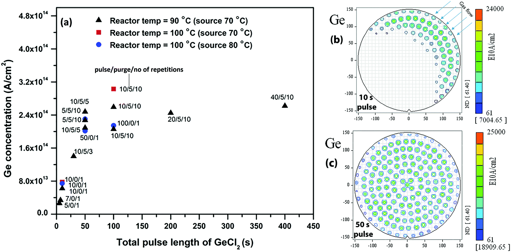 | ||
| Fig. 1 (a) Ge atomic density as a function of the GeCl2·dioxane pulse length, TXRF Ge distribution maps on 300 mm Si wafer with (b) 10 s pulse and (c) 50 s pulse length of GeCl2·dioxane. The TXRF Ge distribution maps correspond to Ge chemisorption at a reactor temperature of 90 °C and a GeCl2·dioxane ampoule temperature of 70 °C. | ||
The Ge saturation coverage of ∼2.7 × 10¹⁴ at cm−2 is only ∼25% of the potentially complete coverage (∼1 × 10¹⁵ at cm−2 atomic density for complete monolayer coverage of Ge). One possibility to explain this low value of the saturation coverage is steric hindrance of the ligands of the chemisorbed species that could shield part of the reactive surface (OH groups) from being accessible to the incoming GeCl2·dioxane reactant. In the case of molecular adsorption (Fig. 2(a)), we assume that the weakly bonded dioxane ligands desorb quickly to be replaced by coordinative bonds with surface oxygen or surface hydroxyl groups, with the formation of GeCl2 surface species. However, the Ge atomic density of 2.7 × 10¹⁴ at cm−2 at saturation is still lower than the maximum Ge content allowed for GeCl2 surface species based on steric hindrance of the Cl ligands. The maximum coverage of Cl using the steric hindrance model on a flat surface has been calculated as 8.8 × 10¹⁴ at cm−2 (8.8 × 10¹⁴ Cl at cm−2 → 4.4 × 10¹⁴ Ge at cm−2).27
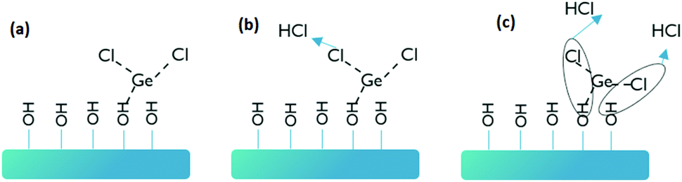 | ||
| Fig. 2 (a) Option1: the GeCl2 molecule absorbs on OH groups based on the steric hindrance model, (b) option 2: the GeCl2 molecule uses one OH group for adsorption, and (c) option 3: the GeCl2 molecule uses two OH groups for adsorption. | ||
In addition, the GeCl2 molecule can undergo ligand exchange reactions with the reactive OH groups, with release of HCl (Fig. 2(b) and (c)). However, these reactions could result in even more accommodation of Ge. We conclude that all reactions shown in Fig. 2 are possible and the saturation coverage cannot be explained by steric hindrance of the Cl ligands. Another possibility is that the coverage is limited by a low density or reactivity of the surface sites.
When the same experiment was repeated with (TES)2Se exposure to a native SiO2/Si surface, it resulted in no detected Se adsorption (TXRF, Fig. S1, ESI†). According to the reported dehalosilylation chemistry17 for growth of GeSbTe, ligand exchange of the alkylsilylchalcogenide precursor occurs with chloride surface species available from the previous GeCl2 reaction. Since no such reactive sites are present on the native SiO2/Si substrate, (TES)2Se is not able to adsorb.
In view of the above, the native SiO2/Si surface was first treated with GeCl2·dioxane. A long GeCl2·dioxane exposure consisting of 500 cycles of GeCl2·dioxane pulse/purge (5 s pulse/5 s purge) was carried out on the SiO2/Si surface to saturate the surface with chloride-reactive GeCl2 species. This indeed provides reactive sites for Se precursor adsorption, as TXRF shows the presence of Se on the surface. Fig. 3 shows the Se concentration as measured by TXRF as a function of the (TES)2Se pulse length on a GeCl2·dioxane pretreated Si/SiO2 surface. The Se concentration saturates only after 400 s of (TES)2Se exposure, irrespective of the different process conditions. We tested similar pulsing sequences for (TES)2Se [continuous dose or pulse/purge/repetition (mentioned in Fig. 3a)], for the reasons as aforementioned for the Ge precursor. We found that the (TES)2Se precursor dose is not decreasing as a function of pulse length (pulse/purge/repetition sequence provides the same Se atomic density as a continuous dose) and a continuous (TES)2Se pulse is providing optimal injection to increase the throughput. The TXRF Se atomic density distribution maps reveal much better within wafer uniformity below the saturation pulse length (0–400 s) as compared to Ge (Fig. 3b). This indicates that Se adsorption on a precoated GeClx surface is limited by a rather low reaction efficiency. The Se saturation content is ∼3.5 × 10¹³ at cm−2, which shows that Se is covering only 15% of the available Ge sites. This low Se content is partly explained by steric hindrance of rather bulky ethyl silyl ligands of (TES)2Se precursor.
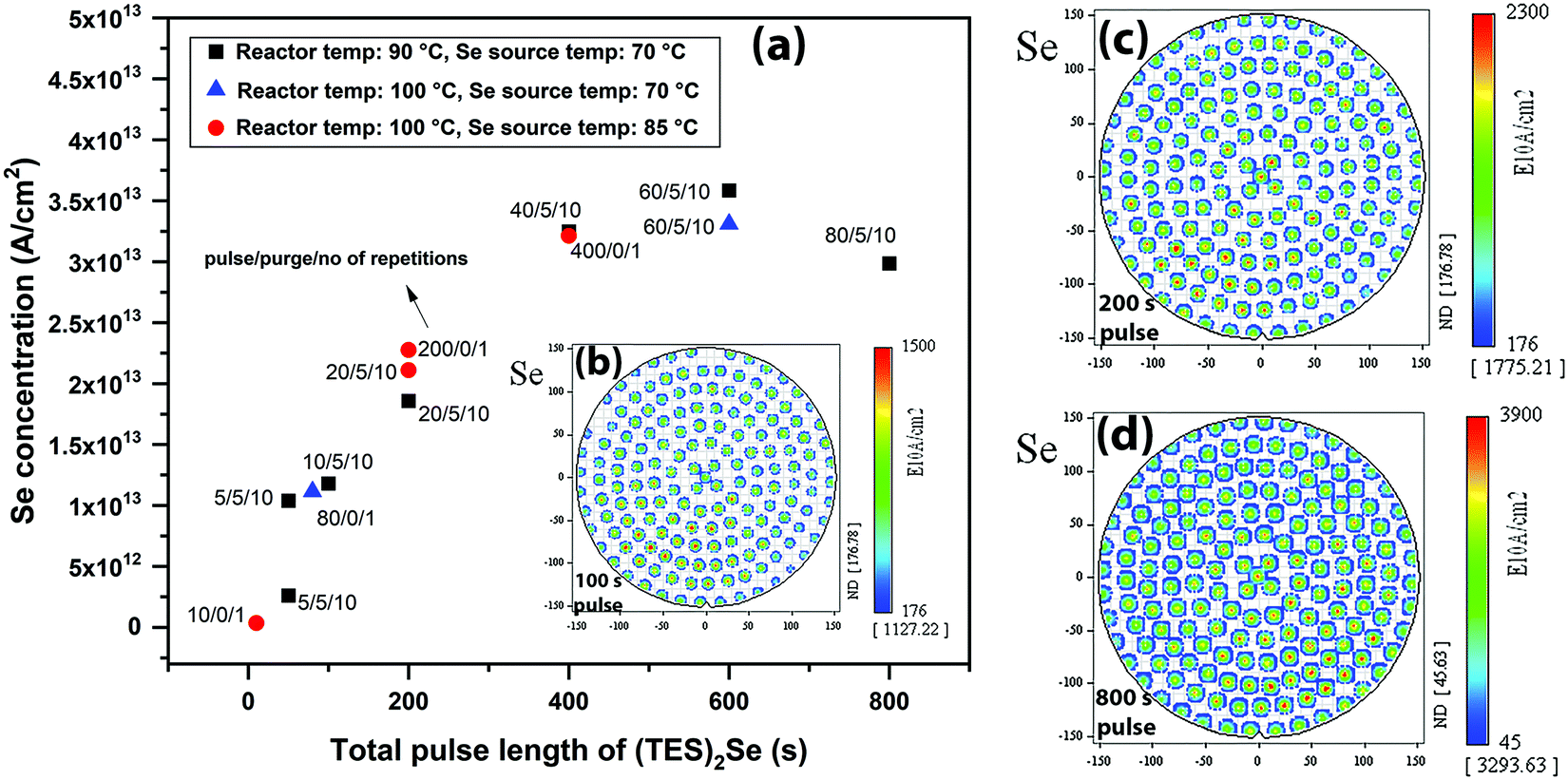 | ||
| Fig. 3 (a) Variation of Se atomic density vs. total pulse length of (TES)2Se, TXRF Se distribution map on 300 mm Si wafer with (b) 100 s pulse, (c) 200 s pulse, and (d) 800 s pulse lengths of (TES)2Se. The TXRF Se distribution maps correspond to Se chemisorption at a reactor temperature of 90 °C and a (TES)2Se ampoule temperature of 70 °C. | ||
Fig. 4 shows the reactor temperature effect on (TES)2Se adsorption. Clearly, Se adsorption decreases at a higher reactor temperature (Fig. 4(a)): ∼64% decrease in Se atomic density is observed, when going from 100 °C to 150 °C reactor temperature. Fig. 4(b) and (c) show the TXRF Se atomic density distribution maps with 80 s of (TES)2Se pulse length at 100 °C and 150 °C reactor temperatures, respectively. A decrease in the presence of Se is also observed in these maps when going to the 150 °C reactor temperature albeit still uniform indicating that it is not the underdosing issue. On the other hand, Ge adsorption did not show any appreciable dependence on the reactor temperature changes in this experiment, which shows that reaction between Ge and Se precursors is favoured in a narrow low temperature window. In the literature,17,18,21 chalcogenide materials grown with the same type of chemistry have shown a decrease in GPC with increase in growth temperature, which has been attributed to desorption of precursors at higher temperature.
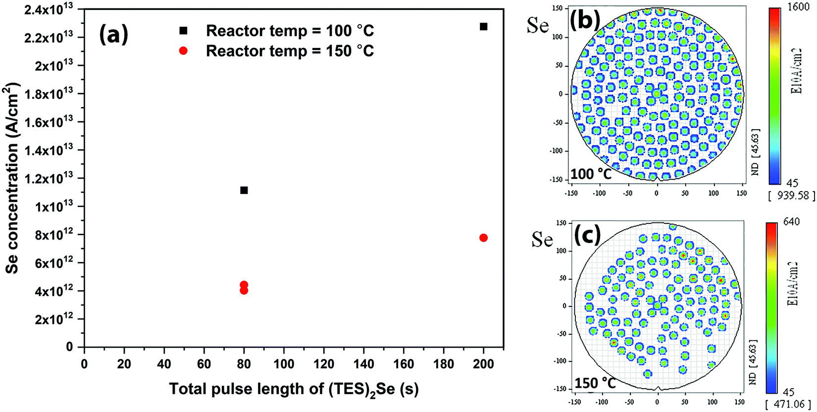 | ||
| Fig. 4 (a) Temperature effect on Se adsorption: variation of Se concentration vs. total pulse length of (TES)2Se at different temperatures. TXRF Se distribution map on 300 mm Si wafer with (b) 80 s pulse at a low temperature, and (c) 80 s pulse at a higher temperature. | ||
The adsorption studies showed that GeCl2·dioxane and (TES)2Se precursor adsorption is very slow, which poses a hurdle for the development of an ALD GeSe process with a decent throughput. Out of these two precursors, particularly (TES)2Se is impractical due to its slow reaction with the GeClx-terminated surface and its low vapor pressure. T. Hatanpää et al. reported thermogravimetric analysis curves for different Te and Se compounds where different compounds including (TES)2Se, (TES)2Te, and (TMS)2Te showed pure evaporation behaviour with minimal residues.28 The vapor pressure of (TMS)2Te was found to be very high compared to (TES)2Te, due to its lower molecular weight. Additionally, TMS has a smaller size compared with TES, which can provide better reactivity and low steric hindrance. This provided good motivation for us to use (TMS)2Se as a Se source in order to make Se adsorption faster. Hence, the next Se adsorption tests were performed using a (TMS)2Se source.
Fig. 5 shows the Se concentration vs. pulse length of the (TMS)2Se precursor as measured via TXRF. For comparison purposes, Se adsorption with (TES)2Se is also shown in the same graph. We employed the same reactor and processing conditions for studying the adsorption of both precursors. It is evident that (TMS)2Se demonstrates faster, higher, and uniform Se saturation concentration with Se saturating with 100 s of (TMS)2Se. The saturation concentration is ∼1.1 × 10¹⁴ at cm−2, which amounts to 75% coverage of available Ge sites. This is significantly higher coverage of available Ge sites compared to that of (TES)2Se (15% Ge site coverage with (TES)2Se). Faster saturation and higher coverage with (TMS)2Se in comparison with (TES)2Se can be attributed to higher vapor pressure, better reactivity, and low steric hindrance (relatively smaller ligands) of the (TMS)2Se precursor. Hence, this study confirms that (TMS)2Se is a better Se precursor for dehalosilylation reaction with metal chloride precursors to form GeSe.
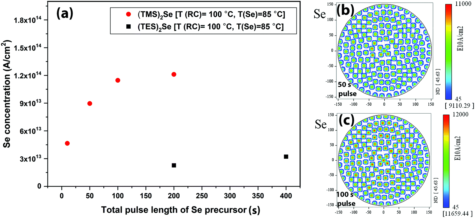 | ||
| Fig. 5 (a) Variation of Se concentration vs. total pulse length of (TMS)2Se and (TES)2Se under the same reactor conditions. TXRF Se distribution map (from (TMS)2Se) on 300 mm Si wafer with (b) 100 s pulse length and (c) 200 s pulse length of (TMS)2Se. | ||
On the other hand, keeping in mind the slow adsorption of GeCl2, the alternative precursors are other Ge halides such as Ge bromide (GeBr2) and germanium iodide (GeI2). However, a study has shown that GeBr2 reaction with alkylsilyl compounds proceeds relatively slowly with more impurities in the final product.28 This was attributed to the soft base character of Br−. The size of the nucleus increases down the group of halides (Cl < Br < I), which makes Br and I softer bases compared to Cl, hence making the reaction of metal bromides and iodides with alkylsilyl compounds less favourable. Therefore, the GeCl2·stabilizer still seems to be the best metal halide precursor for this chemistry to form the GeSe product.
Pulsed CVD process development of GeSe
In this section, we show the development of a pulsed CVD process for GeSe using GeCl2·dioxane and (TMS)2Se. We have investigated the effect of purge length, precursor temperature, and reactor temperature on growth per cycle (GPC) of GeSe. Afterwards, a ∼20 nm GeSe film is grown at a reactor temperature of 70 °C, GeCl2·C4H8O2 temperature of 80 °C, and (TMS)2Se at RT for morphological and compositional characterization.At first, the effect of purge length on GPC of GeSe was investigated and is shown in Fig. 6a. It is evident that GPC increases sharply, while moving to a pulsed CVD regime (zero purge between precursor exposures). Overall, there is 75% increase in GPC, while decreasing the purge time from 5 s to 0 s. In general, purges should not influence the ALD growth regime, if they are enough in removing all the excess precursors and by-products. However, it is seen that GPC of GeSe also decreases in the ALD regime with increase in the purge length. This decrease can be assigned either to incomplete/slow precursor adsorption or involvement of some physisorption. This would imply that unreacted precursor groups sitting on the surface are pushed along with the increase in purge time resulting in a decrease of GPC.
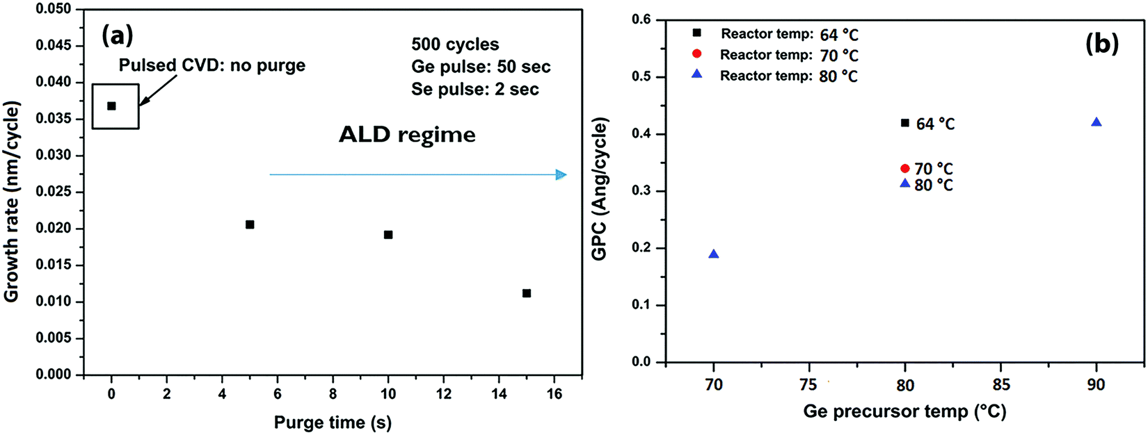 | ||
| Fig. 6 (a) Variation in GPC vs. purge time (s) at a reactor temp. of 70 °C, Ge precursor temperature of 80 °C, and (TMS)2Se at RT, and (b) variation in GPC vs. Ge precursor temperature and reactor temperature. | ||
Fig. 6b shows GPC as a function of Ge precursor temperature and reactor temperature in a pulsed CVD regime. A higher Ge precursor temperature implicates increased delivery of Ge precursor. Increased delivery of GeCl2 precursor brings additional Cl-reactive sites for the ligand exchange reactions with the incoming (TMS)2Se in the next pulse, which results in higher GPC. On the other hand, reactor temperature can also be lowered to increase the GPC of GeSe.
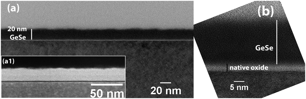
A thick GeSe layer is grown (reactor temp. = 70 °C, GeCl2·C4H8O2 = 80 °C, and (TMS)2Se = RT) to characterize the surface morphology, composition, and crystalline state of the film. For this growth, GeCl2–dioxane and (TMS)2Se pulse times were kept at 25 s and 0.5 s, respectively to increase the throughput of the process. Under these process conditions, we obtain a GeSe GPC of 0.34 Å per cycle. Fig. S2 (ESI†) shows thickness contour maps (ellipsometry mapping with 49 measurement points) revealing the thickness uniformity of the pulsed CVD-grown GeSe film across a 300 mm wafer. The std deviation in thickness is 1.6%, which implies excellent GeSe thickness uniformity across the wafer. Fig. 7a shows a cross-sectional TEM image of the GeSe layer grown on native SiO2/Si. The layer is about 20 nm thick and shows some surface roughness. The inset of Fig. 7a(a1) shows a dark field (DF) TEM image of the same GeSe film. No crystal grains are observed in the film revealing its amorphous nature. The high-resolution TEM image in Fig. 7b confirms the amorphous phase of the as-grown GeSe layer.
 | ||
| Fig. 7 (a) TEM image of GeSe grown on planar Si, inset (a1) DF image of the same sample, and (b) high resolution TEM image of GeSe confirming the amorphous nature of the film. | ||
GeSe was grown on 3D test structures to check the conformality of the film (Fig. 8a). The grown GeSe was found to be exceptionally conformal as revealed by uniform thickness in deep trenches of 3D structures. Although there is a pulsed CVD component involved in the growth, the slow reaction chemistry can lead to excellent conformality. In this case, relatively long reaction time can permit diffusion of the precursor inside the deep trenches of 3D structures allowing for a more conformal deposition. Fig. 8b shows the surface morphology of the film as measured by AFM (left Fig. 8b) and SEM (right Fig. 8b). GeSe has a smooth surface morphology as shown by AFM and SEM images. No grains are visible showing the amorphous nature of the film. AFM showed a RMS surface roughness of ∼0.3 nm. Fig. 8(c) shows EDX elemental maps of Ge and Se obtained from the GeSe thin film sample deposited on Si(100). The colorized maps show strong contrast among Ge and Se and they reveal the uniform elemental distribution along the scanned area.
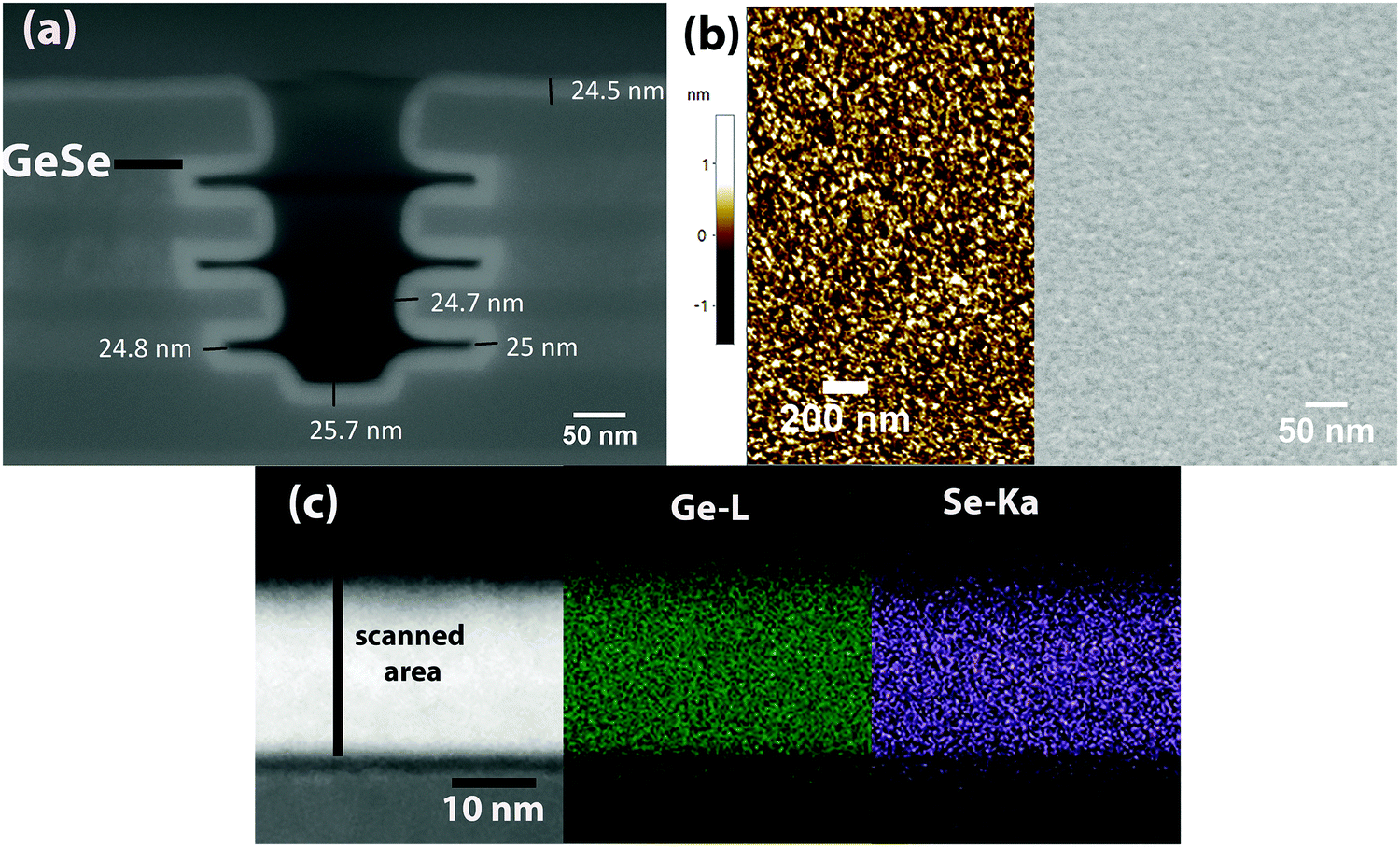 | ||
| Fig. 8 (a) SEM image of GeSe grown on 3D test structures revealing high conformality of the film, (b) morphological characterization of the GeSe film with AFM (left) and SEM (right) showing a smooth surface of the film, and (c) EDX elemental colorized maps revealing the uniform presence of Ge and Se in the grown GeSe. | ||
Fig. S3 (ESI†) shows a cross-sectional EDS line scan from the air–GeSe interface to the GeSe–Si interface. The entire film composition is stoichiometric, except its surface, which is found to be Ge rich. The surface oxygen concentration is also higher, which indicates that there is formation of GeOx at the surface. GeOx formation is probably due to long atmospheric exposure of the film before EDX measurement. An oxygen content of 4% was found inside the GeSe film. As the film was not in situ capped during atmospheric exposure, ambient oxygen can diffuse inside the GeSe film from the air–GeSe interface. Hence, it is difficult to deconvolute the oxygen coming from atmospheric exposure and from reactor and/or deposition itself.
In situ temperature programmed XRD measurements were conducted to study the thermal phase stability characteristics. For this study, SiO2 and TiN were used as substrates as they are the device-relevant substrates. The measurement results are shown in Fig. 9 and the results are summarized in Table 1.
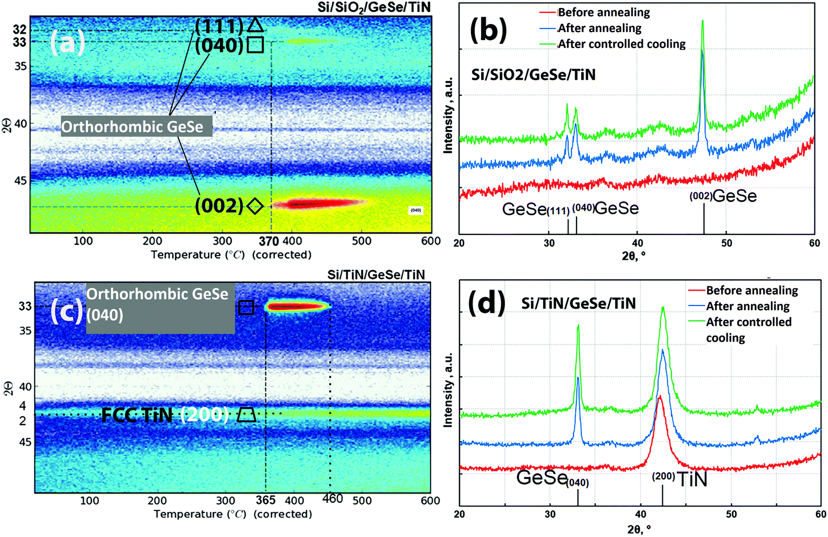 | ||
| Fig. 9 (a) and (c) TXRD 2θ vs. temperature graphs for GeSe grown on SiO2 and TiN revealing the crystallization initiation at ∼370 °C, and (b) and (d) intensity vs. 2θ graphs for GeSe grown on SiO2 and TiN, respectively, revealing the orthorhombic GeSe peaks after annealing the GeSe at 410 °C and cooling it down. | ||
| Substrate | Material | Crystallization temperature (°C) | Peaks | Phase |
|---|---|---|---|---|
| TiN | GeSe | 365 | (040) | Orthorhombic GeSe |
| SiO2 | GeSe | 370 | (111), (040), and (002) | Orthorhombic GeSe |
Fig. 9(a) shows that the GeSe layer on SiO2 crystallizes at temperatures ≥370 °C. The measurement results before annealing, after annealing (at 410 °C), and after cooling the sample are shown in Fig. 9b. The peaks corresponding to the (111), (040), and (002) planes of orthorhombic GeSe are visible after annealing the sample and the same peaks with similar FWHM value persisted after cooling the sample to room temperature. This indicates that the material crystallises at ≥370 °C and remains with the same phase after cooling to RT. For the samples deposited on the TiN substrate, studies were done under annealing conditions the same as those on SiO2 substrates. For examination of the peaks, the sample was heated to 410 °C and a full 2θ scan was performed. XRD patterns before and after the annealing confirm the appearance of a new peak at 33°, (040), which is due to the orthorhombic GeSe phase (see Fig. 9d).
The TiN substrate has a face centered cubic crystalline (FCC) structure, while SiO2 is an amorphous substrate. It is probable that the TiN substrate is acting as a crystalline seed layer to crystallize the GeSe towards a single 040 plane of orthorhombic GeSe. On the other hand, GeSe is crystallizing in various planes of the orthorhombic structure due to the amorphous nature of the SiO2 substrate.
Conclusion
In conclusion, the GeSe deposition process was explored at low deposition temperatures by using GeCl2·C4H8O2 and (TMS)2Se/(TES)2Se as Ge and Se sources, respectively. Ex situ TXRF is found to be a useful technique to gather insights into precursor adsorption kinetics for a process developed in a manufacturing-scale reactor where it is not possible to use conventional in situ characterization techniques like a quartz crystal microbalance (QCM) and spectroscopic ellipsometry.We obtained a GeSe GPC of 0.34 Å per cycle in pulsed CVD mode at a reactor temperature of 70 °C, GeCl2·C4H8O2 temperature of 80 °C, and (TMS)2Se at room temperature. Moving to an ALD regime by including purges between precursor exposures decreases the GPC strongly. However, excellent conformality is obtained in the pulsed CVD regime. Long precursor pulsing times coupled with slow reaction of precursors enabled the conformal GeSe process with reasonable uniformity. This contrasts with the ALD GST process developed in a lab-scale reactor where 1–3 seconds of precursor pulse time was enough to saturate the GST GPC. The GPC is mainly limited by GeCl2 delivery and slow surface reaction kinetics. One option to increase the throughput of the process is by faster injection of the GeCl2 precursor using large area precursor canisters.
Overall GeCl2 + (R3Si)2Se/Te chemistry appears very powerful for both ALD and pulsed CVD of GeSe-and GST-like materials. This has the potential to enable 3D RRAM memory vehicles by combining conformal OTS and phase change memory materials.
Conflicts of interest
There are no conflicts to declare.References
- J. Zhou, S. Member, K. Kim and W. Lu, IEEE Trans. Electron Devices, 2014, 61, 1369–1376 Search PubMed.
- A. Pirovano and K. Schuegraf, Nat. Nanotechnol., 2010, 5, 177–178 CrossRef CAS.
- R. Aluguri and T.-Y. Tseng, IEEE J. Electron Devices Soc., 2016, 4, 294–306 CAS.
- S. R. Ovshinsky, Phys. Rev. Lett., 1968, 21, 1450–1453 CrossRef.
- P. Esqueda and H. K. Henisch, J. Non-Cryst. Solids, 1976, 22, 97–108 CrossRef CAS.
- D. S. Jeong, H. Lim, G. H. Park, C. S. Hwang, S. Lee and B. K. Cheong, J. Appl. Phys., 2012, 111, 102807 CrossRef.
- N. S. Avasarala, G. L. Donadio, T. Witters, K. Opsomer, B. Govoreanu, A. Fantini, S. Clima, H. Oh, S. Kundu, W. Devulder, M. H. Van Der Veen, J. Van Houdt, M. Heyns, L. Goux and G. S. Kar, Dig. Tech. Pap. – Symp. VLSI Technol., 2018, 209–210 Search PubMed.
- N. S. Avasarala, A. Redolfi, S. Kundu, O. Richard, D. Tsvetanova, G. Pourtois, C. Detavernier, L. Goux and G. S. Kar, Phys. Status Solidi RRL, 2017, 21, 92–93 Search PubMed.
- A. Verdy, G. Navarro, V. Sousa, P. Noé, M. Bernard, F. Fillot, G. Bourgeois, J. Garrione and L. Perniola, 2017 IEEE 9th International Memory Workshop IMW, 2017, pp. 4–7.
- A. Velea, K. Opsomer, W. Devulder, J. Dumortier, J. Fan, C. Detavernier, M. Jurczak and B. Govoreanu, Sci. Rep., 2017, 7, 1–12 CrossRef CAS.
- M. J. Lee, D. Lee, S. H. Cho, J. H. Hur, S. M. Lee, D. H. Seo, D. S. Kim, M. S. Yang, S. Lee, E. Hwang, M. R. Uddin, H. Kim, U. I. Chung, Y. Park and I. K. Yoo, Nat. Commun., 2013, 4, 1–8 Search PubMed.
- R. L. Puurunen, J. Appl. Phys., 2005, 97, 121301 CrossRef.
- N. Biyikli and A. Haider, Semicond. Sci. Technol., 2017, 32, 093002 CrossRef.
- S. M. George, Chem. Rev., 2010, 110, 111–131 CrossRef CAS.
- A. Yanguas-Gil, Y. Yang, N. Kumar and J. R. Abelson, J. Vac. Sci. Technol., A, 2009, 27, 1235–1243 CrossRef CAS.
- W.-J. Lee and Y.-H. Choa, J. Vac. Sci. Technol., B: Nanotechnol. Microelectron.: Mater., Process., Meas., Phenom., 2018, 36, 022201 Search PubMed.
- V. Pore, T. Hatanpää, M. Ritala and M. Leskela, J. Am. Chem. Soc., 2009, 131, 3478–3480 CrossRef CAS.
- V. Pore, K. Knapas, T. Hatanpää, T. Sarnet, M. Kemell, M. Ritala, M. Leskelä and K. Mizohata, Chem. Mater., 2011, 23, 247–254 CrossRef CAS.
- T. Eom, T. Gwon, S. Yoo, B. J. Choi, M. Kim, I. Buchanan, S. Ivanov, A. Adamczyk, M. Xiao and C. S. Hwang, J. Mater. Chem. C, 2015, 3, 1365–1370 RSC.
- T. Gwon, T. Eom, S. Yoo, C. Yoo, E. S. Park, S. Kim, M. S. Kim, I. Buchanan, M. Xiao, S. Ivanov and C. S. Hwang, Chem. Mater., 2017, 29, 8065–8072 CrossRef CAS.
- T. Gwon, T. Eom, S. Yoo, H. K. Lee, D. Y. Cho, M. S. Kim, I. Buchanan, M. Xiao, S. Ivanov and C. S. Hwang, Chem. Mater., 2016, 28, 7158–7166 CrossRef CAS.
- T. Eom, T. Gwon, S. Yoo, B. J. Choi, M. S. Kim, I. Buchanan, M. Xiao and C. S. Hwang, Chem. Mater., 2014, 26, 1583–1591 CrossRef CAS.
- T. Eom, T. Gwon, S. Yoo, B. J. Choi, M. S. Kim, I. Buchanan, S. Ivanov, M. Xiao and C. S. Hwang, Chem. Mater., 2015, 27, 3707–3713 CrossRef CAS.
- W. Kim, S. Yoo, C. Yoo, E. Park, J. Jeon, Y. J. Kwon, K. S. Woo, H. J. Kim, Y. K. Lee and C. S. Hwang, Nanotechnology, 2018, 29, 365202 CrossRef.
- E. Langereis, S. B. S. Heil, H. C. M. Knoops, W. Keuning, M. C. M. Van De Sanden and W. M. M. Kessels, J. Phys. D: Appl. Phys., 2009, 42, 073001 CrossRef.
- A. Danel, E. Nolot, M. Veillerot, S. Olivier, T. Decorps, M. L. Calvo-Muñoz, J. M. Hartmann, S. Lhostis, H. Kohno, M. Yamagami and C. Geoffroy, Spectrochim. Acta, Part B, 2008, 63, 1365–1369 CrossRef.
- L. Nyns, A. Delabie, M. Caymax, M. M. Heyns, S. Van Elshocht, C. Vinckier and S. De Gendt, J. Electrochem. Soc., 2008, 155, G269 CrossRef CAS.
- T. Hatanpää, V. Pore, M. Ritala and M. Leskela, ECS Trans., 2009, 25, 609–616 CrossRef.
Footnote |
| † Electronic supplementary information (ESI) available. See DOI: 10.1039/d0ma01014f |
| This journal is © The Royal Society of Chemistry 2021 |