
 Open Access Article
 This Open Access Article is licensed under a Creative Commons Attribution-Non Commercial 3.0 Unported Licence
High carrier mobility and ultralow thermal conductivity in the synthetic layered superlattice Sn4Bi10Se19†
Ruiming
Lu‡
a,
Alan
Olvera‡
a,
Trevor P.
Bailey
 b,
Jiefei
Fu
c,
Xianli
Su
c,
Igor
Veremchuk
d,
Zhixiong
Yin
a,
Brandon
Buchanan
a,
Ctirad
Uher
b,
Xinfeng
Tang
c,
Yuri
Grin
d and
Pierre F. P.
Poudeu
*a
b,
Jiefei
Fu
c,
Xianli
Su
c,
Igor
Veremchuk
d,
Zhixiong
Yin
a,
Brandon
Buchanan
a,
Ctirad
Uher
b,
Xinfeng
Tang
c,
Yuri
Grin
d and
Pierre F. P.
Poudeu
*a
aLaboratory for Emerging Energy and Electronic Materials, Department of Materials Science and Engineering, University of Michigan, Ann Arbor, Michigan 48109, USA. E-mail: ppoudeup@umich.edu; Fax: +1-734-763-4788
bDepartment of Physics, University of Michigan, Ann Arbor, Michigan 48109, USA
cState Key Laboratory of Advanced Technology for Materials Synthesis and Processing, Wuhan University of Technology, Wuhan, Hubei 430070, China
dMax-Planck-Institut für Chemische Physik Fester Stoffe, Nöthnitzer Straße 40, 01187 Dresden, Germany
First published on 2nd March 2021
Abstract
The integration within the same crystal lattice of two or more structurally and chemically distinct building units enables the design of complex materials featuring the coexistence of dissimilar functionalities. Here we report the successful synthesis of single-phase polycrystalline powder of Sn4Bi10Se19, a ternary selenide featuring atomic-scale integration of SnSe-type and Bi2Se3-type building blocks into a large monoclinic unit cell. We found that the complex layered atomic structure along with the large size of the building blocks severely impede the crystallization of an ordered phase. Consequently, the electronic and thermal transport properties of Sn4Bi10Se19 are strongly influenced by the degree of crystallinity and atomic ordering within the crystal lattice. At temperatures below 300 K, the well-crystallized Sn4Bi10Se19 sample displays higher carrier density, carrier mobility, and electrical conductivity compared to the poorly crystallized sample, while both samples show similar electronic properties at high temperatures. Astonishingly, the crystalline sample exhibits up to 30% lower thermal conductivity at 535 K compared to the poorly crystallized sample. This suggests a more efficient phonon scattering at the ordered atomic-scale interfaces between the building blocks in the crystalline sample, owing to bond inhomogeneity and anisotropy, whereas the random orientation of building blocks in the poorly crystallized sample inhibits such effect.
Introduction
Energy conversion from renewable and sustainable sources is necessary to tackle the perpetual growth of the global energy demand. Over the past decades, thermoelectric research has led to the development of several concepts and strategies, such as multicomponent nanostructuring,1 phonon-glass electronic-crystals (PGEC),2 resonant level impurities,3 and electron energy-filtering,4–6 which have enabled the discovery and optimization of a wide range of materials with high figure of merit, ZT = S2σT/κtotal (S is the Seebeck coefficient, σ is electrical conductivity, T is absolute temperature, and κtotal is total thermal conductivity).7–12 However, general and widespread sustainable applications13,14 of thermoelectric technology require the development of low-cost, high-performance materials from abundant and environmentally friendly elements. Therefore, recent trends in thermoelectric research have focused on the development of binary, ternary and quaternary metal chalcogenides.15–17 Their structural diversity and compositional flexibility enable functional properties (thermal, electronic, etc.) engineering through manipulation of the stoichiometry, chemical composition, and distribution of metal atoms in the chalcogenide crystal lattice. For instance, high ZT values were recently reported for chemically simple binary compounds, such as SnSe (ZT ∼ 2.6 at 923 K)17,18 and Cu2Se (ZT ∼ 1.5 at 1000 K),16,19–24 demonstrating promising materials for high temperature power generation applications. The integration of Cu2Se and SnSe phases into (Cu2Se)1−x(SnSe)x bulk composites led to ZT values as high as 1.4 at 825 K.19 However, less attention is allocated to the discovery and optimization of metal chalcogenides for mid-temperature range (300 K to 700 K) and cooling applications. The few notable examples are CsBi4Te6 (ZT ∼ 0.8 at 225 K),25 and various compositions of the solid solution series Bi2−xSbxTe3−ySey.26,27 In addition to the optimization of the thermoelectric properties of known binary and ternary compounds, significant effort is also invested in the search for new metal chalcogenides with increasing compositional, structural and bonding28 complexity, with the goal of creating multifaceted electronic band structures concurrent with ultralow thermal conductivity.15 Along this line, the concept of phase homology is gaining considerable attraction as an elegant approach for the prediction and synthesis of novel promising thermoelectric materials.29–31 The compositional and structural flexibility of homologous structures offer the possibility of engineering the electronic band structure, the inhomogeneity of chemical bonding, which influences the phonon vibration modes of various members of the homologous series, in order to achieve compounds with high thermoelectric performance, i.e. high electrical conductivity (σ) and Seebeck coefficient (S) and ultralow thermal conductivity (K). Several naturally occurring and synthetic mixed-metal chalcogenides homologous series have been reported. These include, Am[M1+lSe2+l]2m[M2l+nSe2+3l+n] (A = K, Rb, Cs and M = Sn, Pb) where l, m, and n represent the size of various structural building units;32,33 [BiQX]2[AgxBi1−xQ2−2xX2x−1]N+1 (Q = S, Se; X = Cl, Br; 1/2 ≤ x ≤ 1);31 the pavonite, MN+1Bi2SN+5 (M = Ag/Bi or Cu/Bi; N ≥ 2);34 and the lillianite, PbN−1−2xBi2+xAgxSN+2,35 and the PbN−1Bi2SeN+236 homologous series, where N = (N1 + N2)/2 representing the average of the number of edge-sharing octahedra running across the central diagonal of the two NaCl-type building units forming the crystal structure. Among these homologous families of complex mixed-metal chalcogenides, phases belonging to the pseudo binary PbSe – Bi2Se3 phase diagram, such as ternary compounds consisting of varying ratios of (PbSe)m(Bi2Se3)n layers37–41 and PbN−1Bi2SeN+2,36 have been attracting considerable attention for thermoelectric application due to their moderately lower electrical resistivity compared to their sulfide analogues. For example, moderate electronic properties and low thermal conductivities have been reported for members of the PbN−1Bi2SeN+2 series, such as Pb5Bi6Se14,42 Pb7Bi4Se13,36 and the recently discovered narrow band gap degenerate n-type semiconductor, Pb6Bi2Se9, with low thermal conductivity (∼1.1 W m−1 K−1 at 300 K) and a moderate figure of merit, ZT ∼ 0.25 at 650 K.43Following the example of the (PbSe)w(Bi2Se3)t family mentioned above, we have recently embarked on the search for new Earth-abundant ternary thermoelectric materials for mid-temperature range applications within the (SnSe)w(Bi2Se3)t system. It is anticipated that in such a system the integration at the atomic scale of structural features from SnSe and Bi2Se3 phases, which are promising thermoelectric materials suitable for applications at high temperatures and below room temperature, respectively, can create compounds suitable for mid-range (300 K to 700 K) power generation application. Early investigations in the SnSe–Bi2Se3 phase space led to the discovery of several ternary compounds, which are structurally related to the lillianite homologous series with general formula MN−1Bi2SeN+2, (M = Sn or (Sn/Bi/□) where □ = vacant site). These include, the Sn2Bi2Se5 (N = 3);44 Sn4Bi2Se7 (N = 5);44 Sn2.22Bi2.52Se6 ≅ (□0.3Sn2.2Bi0.5)Bi2Se6 (N = 4);45 (Sn3Bi2Se6 (N = 4);46 SnBi4Se7 ≅ (□SnBi2)Bi2Se7 (N = 5);44 Sn3.6Bi3.6Se9 ≅ (□1.8Sn3.6Bi1.6)Bi2Se9 (N = 7);45 Sn6Bi2Se9 (N = 7);46 Sn9.52Bi10.96Se26 ≅ (□1.7Sn4.8Bi3.5)Bi2Se13 (N = 11);45 and Sn11.49Bi12.39Se30 ≅ (□2.1Sn5.7Bi4.2)Bi2Se15 (N = 13)45 compounds, which are lillianite phases containing various degrees of structural vacancies. However, these compounds do not contain structural features of the SnSe and/or Bi2Se3 phases, since the lillianite structure is characterized by two alternating NaCl-type slabs (with thickness N1 and N2).
Here, we report on the synthesis, crystal structure and thermoelectric properties of Sn4Bi10Se19, the first vacancy-free example of (SnSe)w(Bi2Se3)t phases with crystal structure consisting of chemically integrated SnSe-type and Bi2Se3-type building units. We found that the Sn4Bi10Se19 phase integrates the high-carrier mobility observed in Bi2Se3 crystals with the low thermal conductivity of SnSe, which makes it an example of a synthetically accessible phonon-glass-electron-crystal (PGEC) superlattice with promising thermoelectric properties.
Results and discussion
Crystal structure
Sn4Bi10Se19 crystallizes in the monoclinic space group C2/m (#12) with lattice parameters a = 28.152(6) Å, b = 4.1567(8) Å, c = 21.242(4) Å, β = 131(3)° and adopts a complex crystal structure, which consists of three distinct building blocks denoted A, B and C (Fig. 1).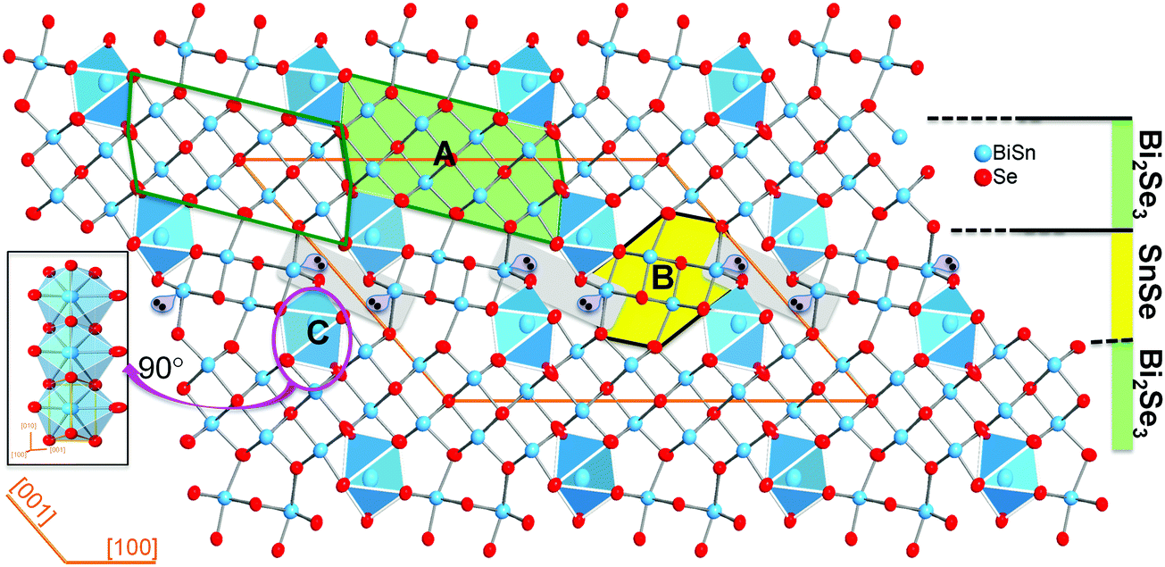 | ||
| Fig. 1 Crystal structure of Sn4Bi10Se19 projected along [010] highlighting the major building blocks: a Bi2Se3-type block denoted A; a SnSe-type block denoted B and a single chain of face-sharing bicapped trigonal prisms denoted C. Adjacent Bi2Se3-type blocks are shifted by one row of metal atoms and share edges of [MSe6] octahedra to form a 2D Bi2Se3-layer parallel to the (001) plane. Adjacent Bi2Se3-layers stacked along [001] are interconnected by SnSe-type blocks to form a 3D crystal structure with open channels that are filled by the single chain of face-sharing [MSe8] bicapped trigonal prisms running along [010]. | ||
The building unit A (Bi2Se3-type) is a cutout from the Bi2Se3 structure and contains two rows of four crystallographically independent metal positions (M1, M2, M4 and M5) that are octahedrally coordinated by Se atoms with various degrees of distortions (Table S1 and Fig. S1, ESI†). The building unit B (SnSe-type) can be extracted from the structure of SnSe and consists of two rows of two crystallographically independent metal positions (M3 and M6) in distorted octahedral geometries. The building unit C is a single chain of face-sharing bicapped trigonal prisms [1+2+2+1+2] around the crystallographically independent metal position, M7. All metal positions in the Sn4Bi10Se19 structure feature Bi/Sn mixed occupancy in various ratios. Details on distortion and M–Se bond distances are found in Table S1 (ESI†). In the three dimensional (3D) structure, the Bi2Se3-type (A) building blocks are interconnected along [100] through edge-sharing M(4)Se6 octahedra to form a two dimensional (2D) sheet parallel to the (001) plane. Adjacent Bi2Se3-type sheets are separated along [001] by discrete SnSe-type (B) building blocks that are terminated at both ends by the building unit C. This atomic scale assembly of the building blocks leads to a structure that resembles a synthetic layered superlattice formed by a 2D Bi2Se3-layer and a 2D SnSe-layer that are stitched together alternatively along [001]. Similar complex structural organization was also observed in compounds such as Cu2Pb6Bi8S19,47 K0.66Sn4.82Bi11.18Se2248 and Sn4.11Bi22.60Se38,49 which is the defect analog of Sn4Bi10Se19. Indeed, both phases (Sn4.11Bi22.60Se38 and Sn4Bi10Se19) share similar lattice parameters and feature mixed occupancy of Sn and Bi at all metal positions. However, while Sn4Bi10Se19 exhibits full occupancy of all metal positions, the Sn4.11Bi22.60Se38 structure contains partially occupied metal positions,49 which seemed to be necessary to maintain the electroneutrality of the compound.45 Based on the final compositions of these two phases, we can establish the narrow solid-solution series of defect compounds with general formula Bi2xSn38−3xSe38, where 10 ≤ x < 38/3. The Sn4Bi10Se19 (x = 10) phase has the stoichiometric composition, whereas the Sn4.11Bi22.60Se38 (x = 11.3) is a defect member containing 5% vacancies at various metal positions.49 Hypothetical compositions with high x values, such as the Sn0.2Bi25.2Se38 (x ∼ 12.6) phase, should display up to ∼10% vacancies at various metal positions in the crystal structure. Such flexibility in the Sn/Bi ratio while maintaining the same crystal structure opens up more opportunities to tune the physical properties.
Synthesis and thermal stability
Despite the interesting crystal structure of the Bi2xSn38−3xSe38 phases, where 10 ≤ x < 38/3, and the prospect for the discovery of high-performance thermoelectric materials, difficulty in synthesizing highly crystalline single-phase samples suitable for measurement of electronic and thermal transport properties has hampered the ability to explore their thermoelectric properties. Achieving highly crystalline samples requires perfect stacking of the 2D Bi2Se3-layer and SnSe-layer into the 3D layered superlattice, which is extremely challenging owing to the complexity of the Bi2Se3-type and SnSe-type building blocks.Therefore, we developed a multistep synthesis procedure for the fabrication of highly crystalline single-phase polycrystalline powder of Sn4Bi10Se19. The structurally disordered but element-homogeneous sample 1 (S1) was initially obtained through solid-state reaction of high-purity elements sealed in an evacuated quartz tube followed by repeated melting and quenching of the product from solid-state reaction using an induction melting furnace. The XRD patterns of the resulting sample S1 showed very poor matching with the theoretical pattern calculated using single crystal structure data (Fig. 2). However, the DSC curves (Fig. S3, ESI†) showed a single broad endothermic peak of melting at around 940 K on heating and a single broad exothermic peak of crystallization with onset at 940 K on cooling. This suggests the formation of a disordered, poorly crystalline Sn4Bi10Se19 with congruent melting upon heating. Using the DSC heating and cooling data from sample S1, several annealing recipes were attempted to achieve highly crystalline samples. The best crystalline samples (S2) were obtained by heating the induction-melted product S1 to 973 K (50 °C above the melting temperature) to achieve a thick molten state, followed by a slow cooling across the crystallization window (973 K to 927 K in 48 hours) in order to allow enough time for self-organization of the large building units. The sample was subsequently held at 927 K, the lower limit of the crystallization window, for another 48 hours and finally cooled to room temperature in 12 hours. A comparison of the XRD pattern of the resulting sample with the theoretical pattern showed excellent matching (Fig. 2B), implying the formation of highly crystalline nearly single-phase samples of Sn4Bi10Se19. A rough analysis of the phase composition of S2 sample suggests that it consists essentially of Sn4Bi10Se19 (53%) and Sn4.11Bi22.60Se38 (42%), which are both members of the solid solutions series Bi2xSn38−3xSe38 discussed above, in addition to metallic Bi (5%) as a minor impurity (Fig. S2, ESI†). The observation of metallic Bi in the sample is consistent with the formation of the Sn4.11Bi22.60Se38 phase, which only seems to stabilize with 5% vacancy at all metal positions.
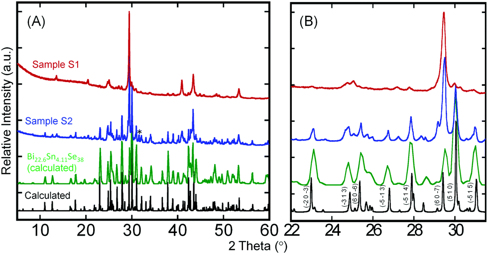 | ||
| Fig. 2 X-Ray diffraction patterns of Sn4Bi10Se19 samples. (A) Comparison of the XRD patterns of the sample S1 obtained after SSR followed by the IMQ process and the sample S2 obtained after the recrystallization process, with the theoretical patterns of Sn4Bi10Se19 and Sn4.11Bi22.6Se38 calculated using single crystal data; (B) enlarged section of the XRD patterns with indexed major diffraction peaks highlighting the excellent match, in peak position, between the XRD pattern of the S2 sample and the calculated patterns. Poorly resolved and missing peaks from the XRD pattern of the S1 sample suggests poor crystallinity. * denotes a peak from metallic Bi as a minor impurity phase. | ||
Interestingly, the S2 sample exhibits similar DSC curves with the disordered poorly crystalline sample S1 (Fig. S3B, ESI†). However, careful analysis of the melting peaks for both S1 and S2 samples (Fig. S3E, ESI†) revealed a single broad peak for poorly crystalline sample, S1, whereas the highly crystalline sample, S2, showed two clear peaks at 935 K and 945 K. The peak at 935 K could be assigned to peritectic formation, whereas the liquidus appears at 945 K. The striking similarity between the DSC curves of samples S1 and S2 despite their quite different XRD patterns indicates that all the chemical bonds and building blocks observed in the crystal structure of Sn4Bi10Se19 are already present in the poorly crystalline sample, S1, obtained through solid-state reaction followed by induction-melting. However, due to the fast-cooling process, the building blocks did not fully order as anticipated from the single crystal structure, hence the formation of the poorly crystallized “amorphous” sample, S1. Upon reheating the sample S1 above the melting temperature and slowly cooling across the crystallization window, the building blocks became mobile again and the ordering process was activated in sample S2. The ability to synthesize both the poorly crystallized (S1) and well-crystallized (S2) samples of Sn4Bi10Se19 enables a unique opportunity to investigate the effect of the evolution of atomic structure ordering on the electronic and thermal transport properties.
Thermal conductivity
Fig. 3 shows the thermal conductivities of both the S1 and S2 samples of Sn4Bi10Se19. It is interesting to note that the poorly crystallized sample (S1) displays a larger total and lattice thermal conductivity than the well-crystallized sample (S2). Nevertheless, both samples exhibit ultralow total thermal conductivity with room temperature values of 0.75 W m−1 K−1 and 0.70 W m−1 K−1 for the S1 and S2 samples, respectively (Fig. 3A). The total thermal conductivity of both samples decreases with increasing temperature, reaching the minimum value of 0.70 W m−1 K−1 and 0.59 W m−1 K−1 at 510 K for the S1 and S2 samples, respectively. The difference is a 16% drop in the total thermal conductivity due to the increased ordering of structural building blocks within the polycrystalline sample. Further increasing the temperature leads to a gradual increase in the total thermal conductivity, which we attribute to bipolar conduction.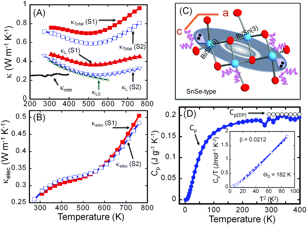 | ||
| Fig. 3 Thermal conductivity and heat capacity of Sn4Bi10Se19. (A) Temperature dependence of the total (κTotal) and lattice (κL) thermal conductivity of the as-synthesized sample (S1) and the sample after recrystallization (S2) compared to the minimum thermal conductivity (κmin) and the theoretical lattice thermal conductivity (κL0); (B) temperature-dependent electronic thermal conductivity (κelec); (C) model of the rattling unit originating from the lone-electron-pair stereoactivity; (D) temperature-dependent heat capacity compared to the Dulong–Petit value. | ||
To understand the origin of the observed drop in the total thermal conductivity, lattice thermal conductivities (κL) were calculated by subtracting the electronic thermal conductivity (κe) from the total thermal conductivity (κL = κtot − κe). The electronic thermal conductivity was calculated using the Wiedemann–Franz law, κe = LσT, where L, σ and T are the Lorenz constant, electrical conductivity and absolute temperature, respectively. Here, we adopt the Lorenz constant value, L = 2.45 × 10⁻⁸ W Ω K−2 given the degenerate semiconducting behavior of the electrical conductivity, for the calculation of the electronic thermal conductivity.
Given the very similar electrical properties of S1 and S2 samples, their electronic thermal conductivities are quite identical regardless of the temperature (Fig. 3B). Therefore, the large difference observed in the total thermal conductivities of the S1 and S2 samples essentially comes from the lattice thermal conductivity (Fig. 3A) influenced by bonding inhomogeneity. The samples display room temperature lattice thermal conductivity values of 0.48 W m−1 K−1 and 0.42 W m−1 K−1 for S1 and S2, respectively. Upon increasing the temperature, the lattice thermal conductivities decrease to ultralow values of 0.37 W m−1 K−1 and 0.26 W m−1 K−1 at 510 K for the S1 and S2 samples, respectively, which is approximately a 30% reduction in the lattice thermal conductivity arising due to the improved crystallinity of the sample. Typically, amorphous materials are expected to display lower thermal conductivity than their highly crystalline counterpart due to increased phonon scattering from the high density of grain boundaries and interfaces arising from short range order, and random distribution or misorientation of structural building units in the polycrystalline sample. To understand the departure from this general trend in the “amorphous” Sn4Bi10Se19 sample, S1, we must first elucidate the origin of ultralow thermal conductivity in the highly crystalline Sn4Bi10Se19 sample, S2. Careful analysis of various coordination polyhedra formed by Se atoms around metal atoms as well as the distribution of the metal–selenium (M–Se) distances within various building blocks in the 3D crystal structure suggests severe local structural distortions (Fig. S1 and Table S3, ESI†). The observed distortion of the coordination polyhedra around Bi atoms in complex selenides typically implies stereochemical activity of the 5s2 lone-electron-pair (LEP). Interestingly, within the 3D structure, the LEPs within the building SnSe-type unit B (Fig. 3C) agglomerate into micelles (highlighted by grey-shaded areas in Fig. 1) with the lobes pointing towards each other. The mutual repulsion between the lobes of the LEPs within individual micellar structure sets in a soft vibrational mode that likely contributes to phonon scattering at the atomic scale. In addition, the repulsion between LEPs induces strong distortion of M–Se bond distances. This leads to strong bond anharmonicity and phonon scattering at the interfaces between various building blocks (A–C) within the crystal structure, which further support the observed ultralow thermal conductivity of the crystalline Sn4Bi10Se19 sample. Alternatively, the low lattice thermal conductivity of Sn4Bi10Se19 can be rationalized by taking into account bonding inhomogeneity and anisotropy within the crystal structure. Indeed, the presence of ordered building units (A–C) with dissimilar chemistries within the structure produces regions with different bonding, which hinder the phonon transport.28
The observed value of the lattice thermal conductivity of the highly crystalline Sn4Bi10Se19 sample, 0.42 W m−1 K−1 at 300 K, was further validated by calculating the theoretical “intrinsic” lattice thermal conductivity (κL0), within the temperature range where only acoustic phonons conduct heat. The theoretical “intrinsic” lattice thermal conductivity (κL0), was calculated (see ESI†) using the Grüneisen parameter, γ = 1.86, obtained from the sound velocity measurement and the Debye temperature, Θ = 182 K, obtained from the heat capacity measurement (Fig. 3D) and sound velocity measurement (Table S4, ESI†). As shown in Fig. 3A, the calculated lattice thermal conductivity, κL0 = 0.42 W m−1 K−1 at 300 K is consistent with the value of the lattice thermal conductivity extracted from the measured total thermal conductivity. In addition, κL0 at various temperatures follows very well, within the temperature range below 550 K, κL extracted from experimental data.
To further benchmark the thermal conductivity of the crystalline Sn4Bi10Se19 sample, the “minimum thermal conductivity”, κmin, was calculated considering that the lattice thermal conductivity reaches the minimum value when the phonon mean-free-path (MFP) (l) is equal to the average of the interatomic distances, using eqn (1).
| κmin = 1/3(Cvνml) | (1) |
For Sn4Bi10Se19, the average interatomic distance is l = 3.06 Å, and the calculated value κmin = 0.26 W m−1 K−1 at 300 K (Fig. 3A) is very similar to the measured lattice thermal conductivity at 510 K for the S2 sample.
It follows from this analysis that the ultralow thermal conductivity observed in Sn4Bi10Se19 results from the combination of (1) local structure distortions due to the stereoactivity of LEPs, (2) inhomogeneity and anisotropy of chemical bonding, (3) the presence of heavy atoms in the crystal structure, (4) low crystal symmetry, and (5) the complexity of the layered 3D superlattice structure, which features a high density of interfaces between building blocks of very different sizes.
In light of the above analysis, we speculate that the rather larger total and lattice thermal conductivity measured from the poorly crystallized sample (S1) arises from the loss of the periodic superlattice arrangements of the Bi2Se3- and SnSe- layers in favor of a more random orientation of various structural fragments formed by the three building blocks A (Bi2Se3-type), B (SnSe-type) and C (chains of face-sharing bicapped trigonal prims around the M7 metal position) as illustrated in Fig. S4 (ESI†). Within this picture, the bonding in the amorphous sample is more homogeneous and less anisotropic due to the building block disorder, which is more favorable to phonon transport.28
Our proposed structure of the poorly crystallized sample (S1) of Sn4Bi10Se19 is supported by both the DSC data and the XRD analysis (Fig. 2 and Fig. S3, ESI†). The similarity in the DSC of S1 and S2 samples suggests that most of the structural building blocks and fragments formed by those building blocks are already present in the poorly crystallized structure. In addition, the presence of many sharp peaks on the XRD patterns of the S1 sample suggests some degrees of atomic ordering, while the poor matching of the diffraction peaks with the theoretical pattern from the single crystal structure analysis indicates lack of long-range order in the S1 sample. The poorly crystalline structure still maintains many of the local atomic-scale structural features that are believed to be responsible for the ultralow thermal conductivity of the well-crystallized sample (S2), which also justifies its ultralow thermal conductivity. However, the lack of (1) inhomogeneity and anisotropy of chemical bonding and (2) high density of interfaces, which would result from the long-range ordering of the building blocks into the observed 3D layered superlattice structure, results in weaker phonon scattering compared to the well-crystallized sample (S2). Consequently, the thermal conductivity of the poorly crystallized sample (S1) of Sn4Bi10Se19 is higher than that of the well-crystallized counterpart (S2).
Electronic properties
To probe the effect of structural ordering on the electronic properties, we have performed the temperature-dependent measurements of the electrical conductivity (Fig. 4A) and Hall effect (Fig. S5, ESI†) on both the S1 and S2 samples in the temperature range from 2 K to 775 K. These data were then used to calculate the variation of charge carrier concentration (n) (Fig. 4B) and charge carrier mobility (μ) (Fig. 4D) with the temperature in both samples. It can be noted that, while both samples exhibit very similar temperature dependence of the electronic properties (n, μ, σ) at temperatures above 300 K, they display remarkably different electronic properties at low temperatures (2 K to 300 K). In general, the electrical conductivity of both samples gradually decreases with rising temperature in the temperature range from 2 K to 500 K, indicating a degenerate semiconducting behavior. However, the rate at which the electrical conductivity drops depends on the temperature range. For instance, a rapid decrease in the electrical conductivity is observed between 2 K and 300 K, which is associated with the sharp drop in the carrier mobility arising from the large increase in the carrier concentration. Indeed the fitting of the temperature-dependent carrier density curve using Arrhenius law (ln(n) ∼ Ea/kBT) suggests the presence, within the band gap (Eg = 0.73 eV), of several impurity states with activation energy, Ea, ranging from 5.6 meV to 130 meV (Fig. 4C). At very low temperatures, a small increase in the temperature leads to the ionization of impurities located at 5.6 meV below the conduction band (CB). Further increase in temperature leads to the ionization of impurities located in deeper states (24 meV and 130 meV). Such thermal activation of carriers from impurity states to the conduction band leads to the observed initial marginal increase in the carrier concentration between 2 K and 500 K.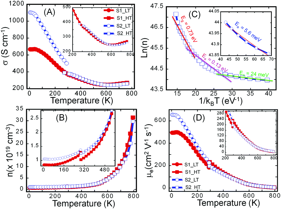 | ||
| Fig. 4 Electronic transport of Sn4Bi10Se19. (A) Temperature-dependent electrical conductivity; (B) temperature-dependent charge carrier concentration; (C) fitting of the carrier concentration using the Arrhenius equation, highlighting the activation energy of impurities and the electronic band gap; (D) temperature-dependent charge carrier mobility. | ||
At temperatures above 500 K, thermal excitation of electrons from the valence band (VB) to the conduction band (CB) leads to a drastic increase in the carrier concentration (Fig. 4B), which is also manifested by the transition of the temperature-dependent electrical conductivity from the heavy-doped semiconducting behavior to intrinsic semiconducting behavior. The above-described trend in the temperature-dependent electronic transport is valid for both the S1 and the S2 samples. The main difference in their electronic properties lies in the magnitude of the electrical conductivity, carrier density, and carrier mobility at various temperatures between 2 K and 300 K. Within this temperature range, the S2 sample displays higher electronic properties (electrical conductivity, carrier concentration and carrier mobility) compared to the poorly crystalline sample (S1). For example, the electrical conductivity at 2 K is ∼1100 S cm−1 for the S2 sample compared to only 700 S cm−1 for the S1 sample. The carrier mobility at 2 K is ∼630 cm2 V−1 s−1 for the sample S2 and 500 cm2 V−1 s−1 for S1 while the carrier concentration at 2 K is 1.1 × 1019 cm−3 for the sample S2 and 8.8 × 1018 cm−3 for the sample S1. The relatively high carrier concentration in both samples is attributed to a doping effect from defects, such as anti-site defects originating from intermixing of Sn and Bi at various metal positions in the crystal structure or the presence of a small fraction of metallic Bi in the S2 sample.
The observed larger values of both the carrier concentration and carrier mobility in the sample S2 compared to S1 implies the presence of surface and interfaces defects in the amorphous samples that contribute to trapping and scattering of charge carriers. The density of those defects is significantly reduced during the recrystallization process leading to the fabrication of sample S2. Upon increasing the temperature, the carrier density in sample S2 increases marginally while the carrier density in sample S1 increases much more rapidly, likely due to the annealing of trapping defects. As a result, very similar carrier density and carrier mobility are achieved in both S1 and S2 samples at temperatures above 500 K, where intrinsic carriers thermally excited from the valence band to the conduction band dominate the electrical conduction. The similarity of electrical properties for both S1 and S2 samples at high temperatures implies similar electronic structures of both materials, which is mainly determined by chemical bonding within the materials. This is consistent with the DSC result where only one melting peak and one crystallization peak were observed in heating and cooling process respectively for both materials. Evidently, all basic chemical bonds and sub building blocks of the Sn4Bi10Se19 structure are formed after induction melting. The subsequent annealing process completed for S2 reactivates the mobility of building blocks locked up at low temperature, to allow them to re-order in a crystalline fashion without breaking apart the chemical bonds.
Although the high temperature electronic properties of both S1 and S2 samples are very similar, low temperature Hall effect measurements (Fig. S5, ESI†) can also probe their intrinsic electrical properties. The low temperature Hall effect data can be divided into two segments, including one below 50 K and the other one from 50 to 300 K. The calculated carrier concentration plateaus below 50 K and thereafter starts to increase with rising temperature for both samples. Such a dual-segment Hall coefficient/carrier concentration indicates doping effects from two kinds of defects: one having shallow defect states and the other having deep defect states within the band gap, which is consistent with our analysis of the temperature dependent carrier concentration. The shallow defect states are excited at extremely low temperature, which was not observed in our Hall effect measurement, and set the initial carrier concentration. The deep defect states are excited at temperatures ranging from 50 K to 300 K.
The combination of ultralow thermal conductivity and high charge carrier mobility in Sn4Bi10Se19 is a hallmark of a promising thermoelectric material. While the ultralow thermal conductivity is attributed to the combination of local structural distortions, the presence of multiple building blocks within the crystal structure, and the presence of a high density of interfaces between the building blocks in all three directions, the observed high charge carrier mobility of ∼250 cm2 V−1 s−1 at 300 K for both samples (S1 and S2) can be attributed to the presence of the 2D Bi2Se3-layer in the 3D crystal structure (Fig. 1), which ensures a high carrier mobility within the ab plane. The observed carrier mobility of Sn4Bi10Se19 is higher than that of polycrystalline n-type SnSe (∼125 cm2 V−1 s−1 at 300 K)50 and comparable to that of polycrystalline n-type Bi2Se3 (∼310 cm2 V−1 s−1 at 300 K)51 with similar carrier concentration (n ∼ 1019 cm−3). Interestingly, the total thermal conductivity of polycrystalline Sn4Bi10Se19 (0.7 W m−1 K−1 at 300 K) is comparable to that of polycrystalline n-type SnSe (∼0.9 W m−1 K−1 at 300 K)50 and is 100% lower than that of polycrystalline n-type Bi2Se3 (1.4 W m−1 K−1 at 300 K).52 Such structurally induced multifunctionalities, where the high carrier mobility of Bi2Se3 is combined with the low thermal conductivity of SnSe, make the Sn4Bi10Se19 phase and structurally related compounds, like Cu2Pb6Bi8S19,47 K0.66Sn4.82Bi11.18Se2248 and Sn4.11Bi22.60Se38,49 great examples of chemically synthesizable phonon-glass electron crystal (PGEC) superlattices suitable for thermoelectric energy conversion.
Both samples (S1 and S2) of Sn4Bi10Se19 show n-type semiconducting behavior, as can be attested to by the negative values of the Hall effect (Fig. S5, ESI†) and Seebeck coefficient (Fig. 5A). The Seebeck coefficients of these samples first increase linearly with increasing temperature, consistent with the heavily doped semiconducting behavior, reach a maximum at 500 K and then drop rapidly with further increase in temperature. The trend is consistent with the temperature dependence of the carrier density. The observed upturn at 500 K in both electrical conductivity and Seebeck coefficient imply bipolar conduction at higher temperature due to the thermal excitation of carriers across the narrow band gap (Eg = 0.73 eV) that is typically reported for Sn–Bi–Se compounds.36,53,54
 | ||
| Fig. 5 Temperature-dependent thermoelectric properties of Sn4Bi10Se19. (A) Thermopower; (B) power factor; (C) figure of merit, ZT. | ||
Due to the similarity in the electrical conductivity and Seebeck coefficient of both samples at high temperatures, comparable power factors (S2σ) were obtained (Fig. 5B). The power factor decreases with rising temperature with a maximum of ∼2.7 μW m−1 K−2 observed at 300 K. The continuous decrease in the power factor with increasing temperature results from the drop in the electrical conductivity near room temperature and the significant degradation of the Seebeck coefficient at temperatures above 500 K. Given the much lower thermal conductivity, the largest figure of merit ZT (Fig. 5C) was observed for the crystalline sample, S2. Due to the combination of decent electronic properties and low thermal conductivity, a peak ZT above 0.2 was obtained at 535 K for the highly crystalline sample, S2, without optimization, making the Sn4Bi10Se19 compound another promising earth-abundant material for thermoelectric application at moderate temperatures.
Conclusion
We have successfully synthesized Sn4Bi10Se19 bulk samples in both poorly crystallized (S1) and well-crystallized (S2) forms using a combination of (1) solid-state reaction (SSR) of the elements at high temperature, (2) induction melting and quenching (IMQ) of the products from SSR, and (3) directional solidification starting from ingots obtained from the IMQ process. Careful investigation of the crystal structure using XRD on single crystals revealed that Sn4Bi10Se19 adopts a complex monoclinic structure consisting of a Bi2Se3-like layer and a SnSe-like layer parallel to the (001) plane that are stacked alternatively along [001] to form a complex synthetic —/Bi2Se3/SnSe/Bi2Se3/— superlattice structure. Interestingly, the complexity of the structural building units renders the crystallization process from the liquid phase extremely challenging. We found that a fast cooling from the molten phase results in the formation of a poorly crystallized sample (S1), whereas slow directional solidification through the crystallization temperature window yields a well-crystallized sample (S2). Electronic transport measurements revealed that while both S1 and S2 samples exhibit similar properties at temperatures above 300 K, the well-crystallized sample S2 displays larger electrical conductivity, carrier density and carrier mobility than the S1 sample in the temperature range from 2 K to 300 K, which is attributed to the decrease in the density of carrier trapping and scattering defects in the S2 sample. Interestingly, a significantly lower total and lattice thermal conductivity was observed for the S2 sample compared to the S1 sample. This is believed to originate from the decrease in (1) the inhomogeneity and anisotropy of chemical bonding and (2) the density of interfaces between building blocks in the S1 sample due to their poor arrangement. However, both the S1 and S2 samples showed ultralow thermal conductivity, which further support the similarity in their atomic structure. Remarkably, the Sn4Bi10Se19 samples (both S1 and S2) integrate the high-carrier mobility observed in Bi2Se3 crystals with the low thermal conductivity of SnSe, resulting in a unique synthetically accessible example of a phonon-glass-electron-crystal (PGEC) superlattice with promising thermoelectric properties. The combination of moderate electronic properties and low thermal conductivity leads to a figure merit, ZT, of ∼0.2 at 535 K for the unoptimized highly crystalline sample. The result highlights the potential of the atomic-scale integration of two or more large building blocks from simple binary compounds, each with dissimilar functionalities (such as high electrical conductivity and ultralow thermal conductivity), into complex superlattices or hierarchical structures as a powerful design approach towards new high-performance multifunctional materials.Author contributions
R. L. and A. O. synthesized the samples, carried out thermoelectric measurements, performed the structural characterization and co-wrote the manuscript. Z. Y. and B. B. helped with sample synthesis, structural characterization, data analysis, and co-edited the manuscript. T. B. and C. U. carried out the electrical conductivity, Seebeck coefficient, and Hall effect measurements and co-edited the manuscript. J. F., X. S. and X. T. synthesized the samples, performed structural characterization, data analysis, and co-edited the manuscript. I. V. and Y. G. performed sample processing, measured thermoelectric properties and co-edited the manuscript. P. F. P. P. conceived the experiment, analyzed the results and co-wrote the manuscript.Conflicts of interest
The authors declare no competing financial interest.Acknowledgements
P. F. P. P. and C. U. acknowledge financial support from the Department of Energy, Office of Basic Energy Sciences under Award #DE-SC0018941 for the investigation of low temperature and high temperature electronic and thermal transports. P. F. P. P. also thanks the Max-Planck-Institut für Chemische Physik fester Stoffe for financial assistance during the sabbatical stay from June to August 2018.References
- A. J. Minnich, M. S. Dresselhaus, Z. F. Ren and G. Chen, Energy Environ. Sci., 2009, 2, 466 RSC.
- A. S. Glen, CRC Handbook of Thermoelectrics, CRC Press, 1995 DOI:10.1201/9781420049718.ch34.
- J. P. Heremans, V. Jovovic, E. S. Toberer, A. Saramat, K. Kurosaki, A. Charoenphakdee, S. Yamanaka and G. J. Snyder, Science, 2008, 321, 554–557 CrossRef PubMed.
- J. P. A. Makongo, D. K. Misra, X. Y. Zhou, A. Pant, M. R. Shabetai, X. L. Su, C. Uher, K. L. Stokes and P. F. P. Poudeu, J. Am. Chem. Soc., 2011, 133, 18843–18852 CrossRef PubMed.
- Y. F. Liu, P. Sahoo, J. P. A. Makongo, X. Y. Zhou, S. J. Kim, H. Chi, C. Uher, X. Q. Pan and P. F. P. Poudeu, J. Am. Chem. Soc., 2013, 135, 7486–7495 CrossRef PubMed.
- P. Sahoo, Y. F. Liu, J. P. A. Makongo, X. L. Su, S. J. Kim, N. Takas, H. Chi, C. Uher, X. Q. Pan and P. F. P. Poudeu, Nanoscale, 2013, 5, 9419–9427 RSC.
- M. S. Dresselhaus, G. Chen, M. Y. Tang, R. G. Yang, H. Lee, D. Z. Wang, Z. F. Ren, J. P. Fleurial and P. Gogna, Adv. Mater., 2007, 19, 1043–1053 CrossRef.
- K. Biswas, J. Q. He, I. D. Blum, C. I. Wu, T. P. Hogan, D. N. Seidman, V. P. Dravid and M. G. Kanatzidis, Nature, 2012, 489, 414–418 CrossRef PubMed.
- P. F. P. Poudeu, J. D'Angelo, A. D. Downey, J. L. Short, T. P. Hogan and M. G. Kanatzidis, Angew. Chem., Int. Ed., 2006, 45, 3835–3839 CrossRef.
- J. R. Sootsman, D. Y. Chung and M. G. Kanatzidis, Angew. Chem., Int. Ed., 2009, 48, 8616–8639 CrossRef.
- G. J. Snyder and E. S. Toberer, Nat. Mater., 2008, 7, 105–114 CrossRef.
- P. F. P. Poudeu, R. Lu, Y. F. Liu, P. Sahoo and A. Page, in Materials Aspect of Thermoelectricity, ed. C. Uher, CRC Press, Taylor and Francis Group, 2016, ch. 7, in print Search PubMed.
- M. N. Leuenberger and D. Loss, Nature, 2001, 410, 789–793 CrossRef.
- M. Mannini, F. Pineider, P. Sainctavit, C. Danieli, E. Otero, C. Sciancalepore, A. M. Talarico, M. A. Arrio, A. Cornia, D. Gatteschi and R. Sessoli, Nat. Mater., 2009, 8, 194–197 CrossRef.
- L. Dawahre, R. Lu, H. Djieutedjeu, J. Lopez, T. Bailey, B. Buchanan, Z. Yin, C. Uher and P. Poudeu, ACS Appl. Mater. Interfaces, 2020, 12, 44991–44997 CrossRef PubMed.
- H. L. Liu, X. Shi, F. F. Xu, L. L. Zhang, W. Q. Zhang, L. D. Chen, Q. Li, C. Uher, T. Day and G. J. Snyder, Nat. Mater., 2012, 11, 422–425 CrossRef.
- L. D. Zhao, S. H. Lo, Y. S. Zhang, H. Sun, G. J. Tan, C. Uher, C. Wolverton, V. P. Dravid and M. G. Kanatzidis, Nature, 2014, 508, 373–377 CrossRef PubMed.
- L. D. Zhao, G. J. Tan, S. Q. Hao, J. Q. He, Y. L. Pei, H. Chi, H. Wang, S. K. Gong, H. B. Xu, V. P. Dravid, C. Uher, G. J. Snyder, C. Wolverton and M. G. Kanatzidis, Science, 2016, 351, 141–144 CrossRef.
- L. L. Zhao, X. L. Wang, J. Y. Wang, Z. X. Cheng, S. X. Dou, J. Wang and L. Q. Liu, Sci. Rep., 2015, 5, 7671 CrossRef.
- D. Li, X. Y. Qin, Y. F. Liu, C. J. Song, L. Wang, J. Zhang, H. X. Xin, G. L. Guo, T. H. Zou, G. L. Sun, B. J. Ren and X. G. Zhu, RSC Adv., 2014, 4, 8638 RSC.
- L. Yang, Z. G. Chen, G. Han, M. Hong, Y. C. Zou and J. Zou, Nano Energy, 2015, 16, 367–374 CrossRef CAS.
- R. M. Lu, A. Olvera, T. P. Bailey, C. Uher and P. F. P. Poudeu, ACS Appl. Mater. Interfaces, 2020, 12, 31601–31611 CrossRef CAS.
- R. Lu, T. Bailey, C. Uher and P. Poudeu, ACS Appl. Energy Mater., 2020, 3, 9133–9142 CrossRef CAS.
- A. A. Olvera, N. A. Moroz, P. Sahoo, P. Ren, T. P. Bailey, A. A. Page, C. Uher and P. F. P. Poudeu, Energy Environ. Sci., 2017, 10, 1668–1676 RSC.
- D. Y. Chung, T. Hogan, P. Brazis, M. Rocci-Lane, C. Kannewurf, M. Bastea, C. Uher and M. G. Kanatzidis, Science, 2000, 287, 1024–1027 CrossRef CAS.
- B. Poudel, Q. Hao, Y. Ma, Y. C. Lan, A. Minnich, B. Yu, X. A. Yan, D. Z. Wang, A. Muto, D. Vashaee, X. Y. Chen, J. M. Liu, M. S. Dresselhaus, G. Chen and Z. F. Ren, Science, 2008, 320, 634–638 CrossRef CAS.
- Y. S. Hor, A. Richardella, P. Roushan, Y. Xia, J. G. Checkelsky, A. Yazdani, M. Z. Hasan, N. P. Ong and R. J. Cava, Phys. Rev. B: Condens. Matter Mater. Phys., 2009, 79, 195208 CrossRef.
- Y. Grin, J. Solid State Chem., 2019, 274, 329–336 CrossRef CAS.
- A. Mrotzek, L. Iordanidis and M. G. Kanatzidis, Inorg. Chem., 2001, 40, 6204–6211 CrossRef CAS.
- H. Ohta, W. S. Seo and K. Koumoto, J. Am. Ceram. Soc., 1996, 79, 2193–2196 CrossRef CAS.
- M. Ruck and P. F. P. Poudeu, Z. Anorg. Allg. Chem., 2008, 634, 482–490 CrossRef CAS.
- M. G. Kanatzidis, Acc. Chem. Res., 2005, 38, 359–368 CrossRef CAS PubMed.
- A. Mrotzek and M. G. Kanatzidis, Acc. Chem. Res., 2003, 36, 111–119 CrossRef.
- B. Makovicky, W. C. Mumme and J. A. Watts, Can. Mineral., 1977, 15, 339–348 Search PubMed.
- A. Pring, M. Jercher and E. Makovicky, Mineral. Mag., 1999, 63, 917–926 CrossRef CAS.
- A. Olvera, G. S. Shi, H. Djieutedjeu, A. Page, C. Uher, E. Kioupakis and P. F. P. Poudeu, Inorg. Chem., 2015, 54, 746–755 CrossRef CAS.
- L. Shelimova, O. Karpinskii, P. Konstantinov, E. Avilov, M. Kretova, G. Lubman, I. Y. Nikhezina and V. Zemskov, Inorg. Mater., 2010, 46, 120–126 CrossRef CAS.
- L. Shelimova, O. Karpinskii and V. Zemskov, Inorg. Mater., 2008, 44, 927–931 CrossRef CAS.
- L. Shelimova, V. Zemskov, E. Avilov, M. Kretova, I. Y. Nikhezina and A. Mikhailova, Inorg. Mater., 2015, 6, 298–304 CrossRef.
- V. Zemskov, L. Shelimova, P. Konstantinov, E. Avilov, M. Kretova and I. Nikhezina, Inorg. Mater., 2011, 2, 405–413 CrossRef.
- Y. Zhang, A. P. Wilkinson, P. L. Lee, S. D. Shastri, D. Shu, D.-Y. Chung and M. G. Kanatzidis, J. Appl. Crystallogr., 2005, 38, 433–441 CrossRef CAS.
- M. Ohta, D. Y. Chung, M. Kunii and M. G. Kanatzidis, J. Mater. Chem. A, 2014, 2, 20048–20058 RSC.
- J. Casamento, J. S. Lopez, N. A. Moroz, A. Olvera, H. Djieutedjeu, A. Page, C. Uher and P. F. P. Poudeu, Inorg. Chem., 2017, 56, 261–268 CrossRef CAS.
- K. Adouby, M. L. E. Moubtassim, C. P. Vicente, J. C. Jumas and A. A. Toure, J. Alloys Compd., 2008, 453, 161–166 CrossRef CAS.
- F. Heinke, P. Urban, A. Werwein, C. Fraunhofer, T. Rosenthal, S. Schwarzmüller, D. Souchay, F. Fahrnbauer, V. Dyadkin and G. Wagner, Inorg. Chem., 2018, 57, 4427–4440 CrossRef CAS.
- K.-B. Chen and C.-S. Lee, J. Solid State Chem., 2010, 183, 807–813 CrossRef CAS.
- D. Topa, E. Makovicky, T. C. Balić-Žunić and P. Berlepsch, Eur. J. Mineral., 2000, 12, 825–833 CrossRef CAS.
- A. Mrotzek, D.-Y. Chung, T. Hogan and M. G. Kanatzidis, J. Mater. Chem., 2000, 10, 1667–1672 RSC.
- F. Heinke, A. Werwein and O. Oeckler, J. Alloys Compd., 2017, 701, 581–586 CrossRef CAS.
- C. Chang, M. Wu, D. He, Y. Pei, C.-F. Wu, X. Wu, H. Yu, F. Zhu, K. Wang and Y. Chen, Science, 2018, 360, 778–783 CrossRef CAS.
- R. Liu, X. Tan, G. Ren, Y. Liu, Z. Zhou, C. Liu, Y. Lin and C. Nan, Crystals, 2017, 7, 257 CrossRef.
- G. Sun, X. Qin, D. Li, J. Zhang, B. Ren, T. Zou, H. Xin, S. B. Paschen and X. Yan, J. Alloys Compd., 2015, 639, 9–14 CrossRef CAS.
- K.-S. Choi, D.-Y. Chung, A. Mrotzek, P. Brazis, C. R. Kannewurf, C. Uher, W. Chen, T. Hogan and M. G. Kanatzidis, Chem. Mater., 2001, 13, 756–764 CrossRef CAS.
- A. A. Kozma, M. Y. Sabov, E. Y. Peresh, I. E. Barchiy and V. V. Tsygyka, Inorg. Mater., 2015, 51, 93–97 CrossRef CAS.
Footnotes |
| † Electronic supplementary information (ESI) available: Experimental details, Tables S1–S4 and Fig. S1–S5, X-ray crystallographic data, in CIF format, for the single crystal structure refinements of Sn4Bi10Se19 (CCDC_1942969) at 300 K. For ESI and crystallographic data in CIF or other electronic format see DOI: 10.1039/d0ma00912a |
| ‡ Contributed equally. |
| This journal is © The Royal Society of Chemistry 2021 |