
 Open Access Article
 This Open Access Article is licensed under a Creative Commons Attribution-Non Commercial 3.0 Unported Licence
Large area growth of SnS2/graphene on cellulose paper as a flexible broadband photodetector and investigating its band structure through first principles calculations†
Venkatarao
Selamneni
 ,
Sayan
Kanungo
and
Parikshit
Sahatiya
*
,
Sayan
Kanungo
and
Parikshit
Sahatiya
*
Department of Electrical and Electronics Engineering, Birla Institute of Technology and Science Pilani Hyderabad Campus, Hyderabad 500078, India. E-mail: parikshit@hyderabad.bits-pilani.ac.in; Tel: +91-040-66303617
First published on 19th February 2021
Abstract
This work demonstrates the solution processed fabrication of a SnS2/graphene (Gr) heterojunction on a biodegradable cellulose paper substrate for its utilization as a broadband photodetector. Graphene was dip coated on cellulose paper followed by the direct growth of SnS2 on Gr/cellulose paper by a hydrothermal method. To study the charge transport mechanism of this unique heterojunction, first principles calculations are performed to theoretically estimate the band gap and the electron affinity values that lead to a detailed understanding of the band alignment in this heterojunction. There are no reports which demonstrate the direct large area growth of SnS2 on cellulose paper to fabricate an efficient broadband photodetector, complemented by a detailed theoretical understanding to understand the underlying physics of this device. The responsivity of the fabricated photodetector was calculated to be 6.98 and 3.67 mA W−1 for visible and UV light illumination respectively suggesting that the device was more responsive towards the visible spectrum when compared to the UV region. The durability of the photodetector was tested by subjecting it to 500 bending cycles wherein a negligible change in the responsivity values was observed. The successful fabrication of a large area SnS2/Gr heterojunction on a low-cost cellulose paper substrate with its performance metrics comparable to a device fabricated using sophisticated techniques is a major step ahead in the development of low-cost photodetectors which finds potential applications in security, visible light communication, etc.
Introduction
Even though there has been a surge of research on the fabrication of photodetectors using different materials,1–6 reports on visible light detection are minimal. Some of the promising candidates are transition metal dichalcogenides such as MoS2, WS2, WSe2, etc. which have excellent visible absorption.7–11 Such materials have their anions packed hexagonally between the metals which are octahedrally coordinated and bonded by weak van der Waals (VdW) forces. Furthermore, their tunable bandgaps offer very exciting electronic and optoelectronic properties. In search of materials with similar exciting properties, tin disulfide (SnS2) has recently gained interest as it exhibits a similar 2D structural motif and a layer dependent tunable bandgap of 2.18–2.44 eV.12 Furthermore, SnS2 has already been reported to have a visible light photon to current conversion efficiency of 38%.13 Even though such exciting properties of SnS2 are studied, a flexible broadband photodetector utilizing SnS2 remains unexplored.As a basis of sustainable technology, there has been active research on the fabrication of electronic devices on a paper substrate and is termed as papertronics.14 It offers advantages in terms of low-cost, high availability, mechanical flexibility and most importantly biodegradability. Furthermore, paper based devices are highly biocompatible and find potential applications in wearable electronics. To date, there have been reports on paper based devices for applications in supercapacitors, field effect transistors, photodetectors, batteries, solar cells, etc.15–17
There are various reports that study the synthesis and fabrication of SnS2 based devices for various applications, including the sol–gel method, chemical vapour deposition, hydrothermal method, chemical vapour transport, etc.18–20 Chemical vapour deposition is a widely used method for the deposition of single layer SnS2.21 But utilizing CVD, the growth of SnS2 on the desired substrate is not feasible due to its high temperature requirement. Furthermore, it involves a tedious transfer process which leads to variation in device to device performance. Among the above mentioned methods, the hydrothermal method is more versatile as it offers the possibility of fine tuning the morphology and phase by adding various surfactants and/or adjusting the pH of the nutrient solution. Even though there are reports which utilize the hydrothermal method for the synthesis of SnS2, direct deposition of SnS2 on flexible substrates still remains a challenge.
Graphene, a 2D wonder material has been utilized as a transport material in photodetectors due to its excellent electron and hole mobility.22 Furthermore, the work function of graphene plays an important role in the fabrication of highly responsive photodetectors when used in conjunction with active materials, as the graphene work function is less than those of most of the active transition metal dichalcogenides which allows the transfer of photogenerated carriers to graphene and due to its excellent electronic properties in terms of mobility, there is an effective capturing of photogenerated carriers. SnS2 has a layer dependent bandgap and has already been reported to have a visible light photon to current conversion efficiency of 38%. But pristine SnS2 is not suitable for photodetection as it suffers from the issue of recombination. Hence there is a need of a heterostructure. Graphene has a high carrier mobility and at the same time the work function of graphene is less than the electron affinity of SnS2 which makes graphene a good transport material for SnS2. Furthermore, graphene is p-type which creates local heterojunctions and built-in electric fields which assist in the effective separation of photogenerated carriers.
This report is the first demonstration of a novel SnS2/Gr on cellulose paper based wearable broadband photodetector. The fabrication of photodetector involves two steps, first being, the dip coating of graphene on cellulose paper followed by the direct growth of SnS2 on Gr/cellulose paper. The fabricated photodetector exhibited broadband absorption ranging from the ultraviolet (UV) to visible range as also evident from its absorbance spectra. The responsivity values of the photodetector were found to be 3.67 and 6.98 mA W−1 towards UV and visible light illumination, respectively, suggesting that the fabricated device was more sensitive to visible light compared to UV, which is in agreement with the absorption spectra. Also, density functional theory (DFT) calculations were performed to understand the band structure of SnS2/Gr to gain actual insight into the charge transport phenomenon. Furthermore, since the photodetector was fabricated on flexible cellulose paper, it not only makes the design cost-effective but also environmental friendly, thereby reducing electronic waste. To the best of the author's knowledge, this is the first report on a flexible SnS2/Gr on cellulose paper based broadband wearable photodetector.
Experimental section
Materials and characterization
Tin tetrachloride (SnCl4) and thioacetamide (CH3CSNH2) were procured from Sigma Aldrich. Graphene powder of flake size ∼8 nm was purchased from Graphene Supermarket. All chemicals were used as received. Structural characterization was performed using an X’Pert Pro X-ray diffractometer (XRD) with Cu Kα radiation. Field emission scanning electron microscopy (FESEM) analysis was performed using a ZEISS Ultra-55 SEM to study the morphology. The chemical composition of the active material was further confirmed by X-ray photoelectron spectroscopy (XPS) using a Thermo Scientific K-Alpha XPS system. Raman spectroscopy measurements were taken using a SenterrainVia opus (Bruker) spectrometer at an excitation length of 532 nm. UV-visible-NIR spectra were obtained using a LAMBDA UV/vis/NIR spectrophotometer (PerkinElmer). Electrical measurements were carried out with a Keithley 2450 source meter.Synthesis of SnS2/Gr on cellulose paper
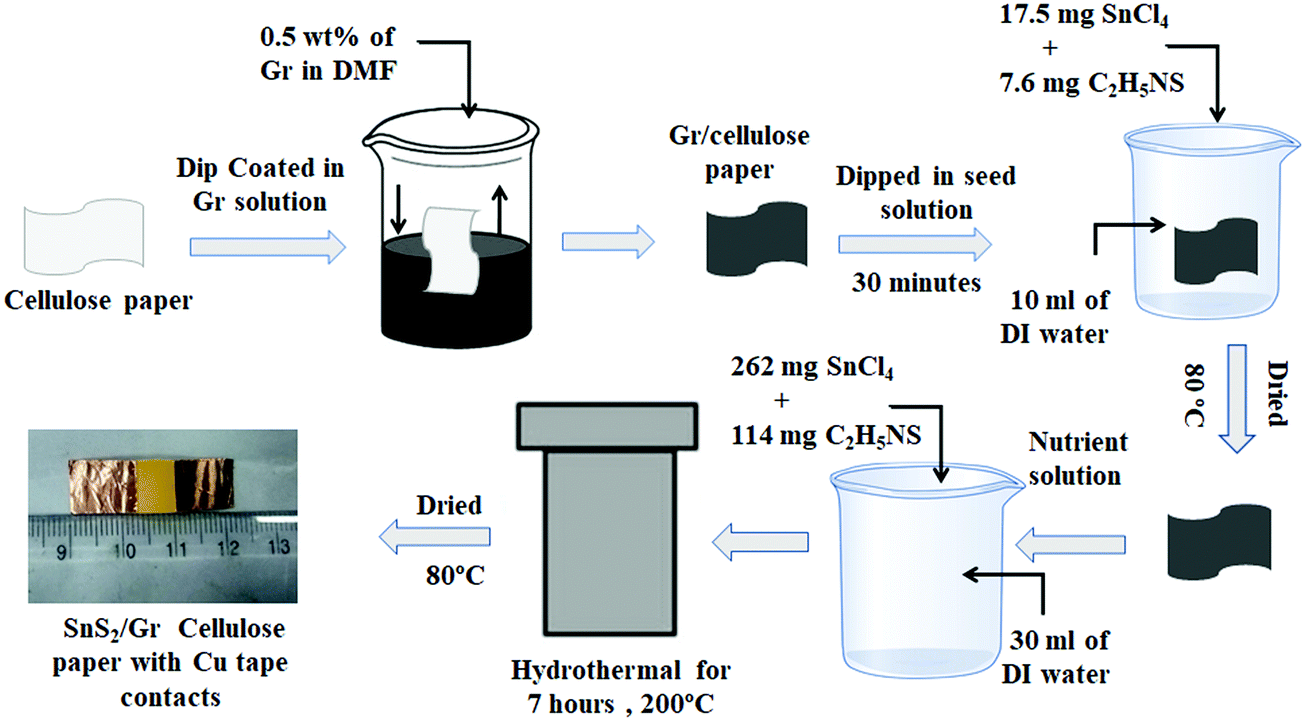 | ||
| Fig. 1 Schematic of the synthesis and fabrication of SnS2/Gr on cellulose paper. | ||
Results and discussion
The hydrothermal process provides the feasibility of tuning the morphologies by adjusting the pH and upon addition of the surfactant. Herein, CTAB was used as a surfactant to increase the surface area. The structural characterization of the as grown SnS2 on Gr/cellulose paper was performed using Field Emission Scanning Electron Microscopy (FESEM). Fig. 2a shows the low magnification FESEM image that reveals the formation of a 3D micro-flower (2–3 μm) like morphology with individual SnS2 nanoflakes. Fig. 2b shows the high magnification FESEM image wherein each 3D micro-flower consists of many individual SnS2 nanoflakes 8–10 nm in size. These individual nanoflakes aggregate and self-assemble to form an intertwined morphology thereby leading to a micro-flower like morphology. The temperature and pressure inside the hydrothermal chamber are suitable such that the micro-flower morphology of SnS2 attains a stable energy level and hence even after removal of SnS2 the stability of the synthesized SnS2 is intact.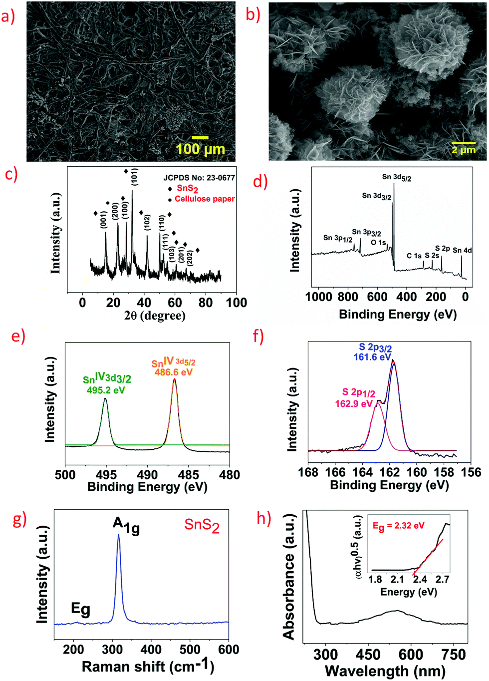 | ||
| Fig. 2 (a and b) Low and High magnification FESEM images of SnS2 on cellulose paper, (c) XRD pattern of SnS2 on cellulose paper, (d) XPS spectra of SnS2 on cellulose paper, (e) deconvolution spectra of Sn 3d, (f) deconvolution spectra of S 2p, (g) Raman spectra of SnS2, and (h) UV-visible spectra of SnS2 grown on paper, inset is the Tauc plot showing the bandgap of ∼2.32 eV. | ||
Based on the observations from FESEM, the 3D SnS2 micro-flower morphology can be explained by the formation of 2D nanoflakes and subsequent aggregation of individual SnS2 nanoflakes into 3D SnS2 micro petals. It is already known that the concentration of sulphur plays a crucial role in the growth and assembly of SnS2 nanostructures. The seeding process can be defined as
| CH3CSNH2 + H2O → CH3COOH + H2S |
| H2S → 2H+ + S2− |
| Sn4+ + S2− → SnS2 |
The precipitation of the metal sulphides by thioacetmaide occurs via the hydrolysis reaction at a relatively low pH which is due to the utilization of thioacetamide. The reaction yields hydrogen sulphide (H2S) followed by the formation of SnS2 nuclei. This supersaturated solution under hydrothermal conditions nucleates further, growing into 2D nanoflakes due to the anisotropic crystal structure of SnS2. The nucleation converts into self-assembly and eventually the aggregation of 2D nanoflakes of SnS2 yields SnS2 with a micro flower like morphology under prolonged hydrothermal conditions (200 °C, 24 h).
The crystal structure of the as synthesized SnS2 was studied using X-ray Diffraction (XRD). Fig. 2(c) shows the XRD graph of SnS2 wherein all the crystal planes are well matched with the JCPDS no 022-09511.23
To further study the chemical composition and the oxidation states of the as synthesized SnS2, X-ray photoelectron spectroscopy (XPS) analysis was performed. Fig. 2d shows the survey spectra of SnS2 wherein the presence of Sn, S, O and C elements was observed. Carbon is present due to the stub used for performing the XPS measurements wherein oxygen is present due to the partial oxidation of SnS2 upon exposure to atmospheric conditions. Fig. 2e shows the deconvolution spectra of Sn wherein intense peaks at 486.6 and 495.2 eV are observed which are the characteristic peaks of Sn 3d5/2 and Sn 3d3/2. The two peaks are separated by an energy difference of 8.4 eV, which clearly defines the oxidation state of Sn4+ in SnS2. Fig. 2f shows the deconvolution spectra of S 2p wherein two spin orbital coupling peaks at 161.6 and 162.9 eV were observed, which suggests the S2− state of S. In the XPS survey spectra, the deconvoluted graph of both Sn and S are in good agreement with the reported literature.24 To study the chemical composition, Raman spectroscopy was performed for SnS2 grown on cellulose paper as shown in Fig. 2g. Two peaks are visible, one intense peak at ∼315 cm−1 and a weak broad peak at ∼210 cm−1, representing out-of-plane A1g and in-plane Eg modes, respectively, of 2H-SnS2. Furthermore, the A1g peak at ∼315 cm−1 suggests that the SnS2 grown is a trilayer SnS2.25 The optical bandgap of SnS2 was evaluated using UV-vis spectroscopy. Fig. 2h shows the UV-vis spectrum of SnS2 where it exhibits strong absorbance in the visible range (∼420 nm to 630 nm) and a weak absorption in the UV range. The bandgap of the synthesized SnS2 was calculated using the Tauc plot and it was found to be ∼2.32 eV, as shown in the inset of Fig. 2h.
Fig. 3a and b show the current–voltage (I–V) characteristics of SnS2/graphene with the contacts fabricated on graphene and as can be seen from the figure the fabricated device exhibited excellent ohmic characteristics. The devices were kept in the dark for 12 h before the photodetection measurements were performed so as to stabilize the device. The wavelengths of the ultraviolet and visible light utilized were 365 and 554 nm, respectively. As can be seen from Fig. 3a, an increase in the photocurrent was observed as the visible light illumination intensity increased. This can be attributed to the generation of the electron–hole pairs and the effective separation of the same. Similar observations were observed for UV light illumination, as shown in Fig. 3b. It should be noted that at the visible and UV illumination intensity of 0.198 mW cm−2, 84% and 38% increment in the photocurrent was observed, respectively, suggesting that the fabricated device was more responsive towards visible light when compared to UV light. Fig. 3c shows the temporal response of the fabricated device towards visible light illumination wherein upon increasing the intensity of the incident light, increment in the photocurrent was observed, which is consistent with the I–V data. A similar experiment was repeated for UV light illumination and observations were consistent with the I–V measurements, as shown in Fig. 3d. Furthermore, to verify the repeatability of the fabricated sensor the temporal response of the SnS2/Gr device under visible light illumination, the light source was turned “ON” and “OFF” repeatedly 6 times. As can be seen in Fig. 3e, as the illumination source was turned “ON”, an increase in the photocurrent was observed and as the light source was turned “OFF”, the photocurrent started to decrease in an exponential manner and reached its initial state. A similar experiment was performed for UV light illumination and the results are as shown in Fig. 3f. The experiments were repeated for 3 independent devices and similar results were observed. The response time of the sensor is one of the important figures of merit in analysing how fast the sensor is able to respond to the stimuli and is calculated as the time taken by the sensor to reach from 10% to 90% of the final value. Fig. 3g shows the graph which displays the response time of the fabricated photodetector under visible light illumination and as can be observed, the calculated value is ∼4.53 s which is comparable and even better than some of the photodetectors fabricated in a sophisticated cleanroom environment. Similarly, a rise time of ∼5.41 s was calculated for the device under UV light illumination, Fig. 3h. This further suggests that the fabricated sensors are not only more responsive towards visible light but also respond more quickly when compared to UV light illumination.
 | ||
| Fig. 3 (a and b) IV characteristics of SnS2/Gr under different visible and UV illumination, (c and d) temporal response of SnS2/Gr under different intensities of visible and UV illumination, (e and f) temporal response of SnS2/Gr under constant intensity visible and UV illumination (0.35 mW cm−2), and (g and h) a graph showing the rise time under visible and UV illumination. | ||
Responsivity and external quantum efficiency are two important metrics for a photodetector and are a measure of the photocurrent generated per unit area upon incident light of per unit power. The responsivity and EQE are given by following equations26,27


where, Iλ, Pλ, A, Idark and e are photocurrent, incident power, active area of the device, dark current, and electron charge, respectively. Fig. 4a and b show the responsivity graph of the SnS2/Gr photodetector under both visible and UV light illumination, the responsivity value calculated for visible light illumination was 6.98 mA W−1 and for UV light illumination was 3.67 mA W−1. Therefore, it can be inferred that the fabricated photodetector was 90% more responsive towards visible light when compared to UV light which is consistent with the temporal response data. Fig. 4c and d show the EQE vs. intensity graph wherein the observed value for EQE is 0.016%. As the intensity increases, both responsivity and the EQE decreases which can be attributed to the fact that the difference in the photocurrent and the dark current is less than the difference in the intensities utilized and is consistent with the previous reports.27–29 Specific detectivity of the fabricated photodetector was calculated to be 5.26 × 10⁹ Jones and 1 × 10¹⁰ Jones, for UV and visible light illumination, respectively, as illustrated in Fig. 4e, wherein a decreasing trend is observed with an increase in intensity similar to the responsivity graph shown in Fig. 4a and b. Furthermore, stability of the fabricated device was studied for few days and negligible change in the responsivity value was observed, as shown in Fig. S1 (ESI†), suggesting that the fabricated devices possess excellent stability. Also, the response spectrum is a key parameter of the photodetector. The response spectrum (responsivity vs. wavelength) of the fabricated photodetector is shown in Fig. 4f.
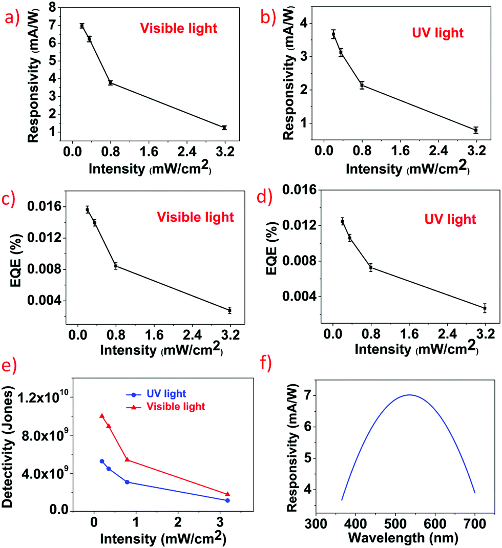 | ||
| Fig. 4 (a and b) Responsivity vs. intensity of the fabricated photodetector under visible and UV illumination, (c and d) graph of EQE vs. intensity under visible and UV light illumination, (e) graph displaying the specific detectivity (D*) of the fabricated SnS2/Gr based photodetector at different intensity UV and visible light illumination and (f) the response spectrum of the fabricated photodetector over UV and visible regions. | ||
The reason for the higher responsivity towards visible light of the fabricated device can be attributed to the higher absorbance in the visible region when compared to the UV region as evident from UV-visible spectroscopy. Compared to the other photodetector fabricated using sophisticated techniques on highly smooth and defect free substrates, the responsivity value calculated for the fabricated photodetector was found to be low.30,31 The reason for the low responsivity value can be attributed to the extremely rough surface of cellulose paper which hinders the mobility of the photogenerated carriers thereby leading to a lesser collection of the carriers at the metal, decreasing the overall responsivity. The other reason is the lack of highly crystalline nature of the SnS2 grown on Gr. The crystallinity, however, can be increased by increasing the processing temperature which will not allow the direct growth of SnS2 on Gr/cellulose paper. However, it should be noted that even though the calculated value was less it was found to be comparable and even higher than those in the reports available on photodetectors on flexible substrates.
Similar experiments were repeated for pristine SnS2 and the responsivity and the EQE graphs for the same can be found in ESI† Fig. S2. It was observed that for pristine SnS2, responsivity and the EQE values were ∼30% less when compared to the SnS2/Gr device under visible and UV light respectively. The reason for the lower responsivity can be attributed to the recombination of the photogenerated carriers due to the lack of sufficient electric field for effective separation. For pristine SnS2, the electric fields are present only at the SnS2/metal junction and hence only the photogenerated carriers generated in the vicinity of the SnS2/metal junction will be effectively separated. For the regions away from the SnS2/metal contact, due to the lack of electric field, the photogenerated electron–hole pairs tend to recombine thereby reducing the responsivity and the EQE. Hence the need for a transport material arises (graphene) which can effectively capture the photogenerated carriers and transport them towards the metal for collection.
To demonstrate the robustness of the fabricated SnS2/Gr flexible photodetector on cellulose paper, it was subjected to bending cycles, and the responsivity values were calculated. It should be noted that the device was bent and then bought to its initial position and the responsivity value was measured. As can be seen in Fig. 5, negligible changes in the responsivity and the EQE values were observed, which suggests that the fabricated device performance does not deteriorate with external bending. Digital images of the fabricated sensor in the bending state are included in the ESI,† Fig. S3.
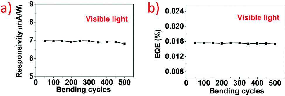 | ||
| Fig. 5 (a) Responsivity vs. intensity graph under different bending cycles and (b) EQE vs. intensity graph under different bending cycles. | ||
To fully understand the band structure of these heterostructures and charge transport mechanism, it is very important to extract the electronic properties through first principles simulations. Most of the reported research on photodetectors makes use of the available values of electron affinity and the work function thereby creating an estimated band diagram which affects the physical understanding and also the hypothesis of the charge transfer mechanism. In this report, to study the electronic properties of the Gr/SnS2 heterostructure and to gain a detailed understanding of the charge transfer mechanism, first principles calculations were performed using the commercially available Atomistix ToolKit (ATK) and Virtual NanoLab (VNL) simulation package from Synopsys QuantumWise.32 Graphene (Gr) and tin disulfide (SnS2) have a hexagonal crystal lattice structure and are considered in their bulk and tri-layer (3L) configurations. The 3L configurations are considered as the experimentally studied materials in this work. To avoid the artificial interactions from the periodic images in the out-of-plane directions, a vacuum of 40 Å was considered in these directions. Initially, the individual configurations were relaxed using geometry optimization with LBFGS methods within the force and pressure tolerance of 0.01 eV Å−1 and 0.0001 eV Å−3, respectively. For density functional theory (DFT) calculations, the linear combination of atomic orbitals (LCAO) basis set has been considered with the density mesh cut-off of 125 Hartree, and the Brillouin zone was sampled using a Monkhorst–Pack grid of 12 × 12 × 1. For structural optimizations, the Local Density Approximation (LDA) method is considered with the Perdew–Zunger (PZ) exchange correlation functional. The detailed results of structural optimizations are tabulated in Table 1. In this context, it should be noted that no significant change in the in-plane lattice constants has been observed for Gr and SnS2 in their bulk and tri-layer configurations. Table 1 clearly indicates that because of the LDA-PZ based structural optimization, the in-plane lattice parameter (a) values are in very good agreement with experimental results, whereas, the out-of-plane lattice parameter (c) values are slightly (<5%) underestimated. However, the overall results also closely match the previously reported lattice parameters of graphite and bulk-SnS2 based on LDA.
Next, DFT calculations are performed on the optimized structures using the Generalized Gradient Approximation (GGA) method using the Perdew, Burke and Ernzerhof (PBE) exchange correlation functional. Furthermore, the empirical correction based on Grimme's DFT-D2 methods was incorporated to account for the weak van der Waals forces between the layers.12 In this context, it should be noted that no spin–orbit interaction was incorporated as it shows insignificant influence on band structures of Gr and SnS2.12 Furthermore, for calculating electron affinities, additional LCAO basis functions above the surfaces as well as multi-grid Poisson solver with the Dirichlet boundary condition for the out of plane directions has been considered to ensure smooth decay of the surface charge density into the vacuum.32 Subsequently, the calculated electron affinity values for SnS2 and Gr were found to be 4.06 and 4.478 eV, respectively, which are in good agreement with the experimentally reported values of 4.1613 and 4.514 eV,34 respectively. The detailed results of electronic band-gaps obtained for bulk and trilayer (3L) SnS2 are tabulated in Table 2.
| Material | DFT method | Indirect band gap (eV) | Reported indirect band gap (eV) | Direct band gap (eV) | Reported direct band gap (eV) |
|---|---|---|---|---|---|
| Bulk-SnS2 | Meta-GGA (TB09) | 2.18 | Experimental | 2.87 | Experimental |
| 2.1812 | 2.8812 | ||||
| DFT (HSE) | DFT (HSE) | ||||
| 2.1812 | 2.6112 | ||||
| 3L-SnS2 | Meta-GGA (TB09) | 2.26 | DFT (HSE) | 2.68 | DFT (HSE) |
| 2.2912 | 2.5412 |
It is well known that the GGA-PBE method underestimates the experimentally observed energy band-gaps of semiconductors principally due to the self-interaction of electrons.12,35 Subsequently, in this work, the calculated direct (1.60 eV) and indirect (1.27 eV) band-gaps using the GGA-PBE-D2 method are found to be well below the experimental values of SnS2. To address this limitation, the meta (M)-GGA method with Tran–Blaha (TB09) exchange–correlation functional has been incorporated which significantly improves the band-gap estimation capacity for a wide range of materials without any significant computational cost.32 Subsequently, in this work, the band-gap values of bulk-SnS2 is calibrated with the experimental results by carefully adjusting the ‘c’ parameter in the MGGA-TB09 method. The same c-parameter is used to obtain the electronic band-structure of 3L-SnS2. Furthermore, the MGGA-TB09 method is also adopted for Gr that shows no observable change in energy band-profiles compared to those in the GGA-PBE method.
Fig. 6a indicates that pristine Gr exhibits a semi-metallic nature with a zero energy band-gap, and the electronic states near the conduction band minima (CBM) and valence band maxima (VBM) are populated by the p-orbitals of carbon. On the other hand, pristine SnS2 shows a clear semiconducting band-gap where the p-orbitals of sulfur and s-orbital of tin populate the states near the CBM, and the s-orbital of tin and p-orbitals of sulfur populates the states near the VBM, as shown in Fig. 6b. Such trends are also consistent with the previous first principles based reports on Gr and SnS2.32,35,36 The theoretically calculated energy band-gaps and electron affinities of Gr and SnS2 can be exploited to visualize the energy band profile of the SnS2/Gr heterostructure. The as-grown SnS2 and Gr show n-type and p-type characteristics, respectively, forming an n–p heterojunction between these materials. The optoelectronic behaviour of the SnS2/Gr can be better understood by analysing the band diagram of the heterojunction and also the charge transfer schematic shown in Fig. 6c. At the interface of SnS2 and Gr, the flow of electrons from SnS2 to Gr results in the alignment of the Fermi level at equilibrium and thereby the development of built-in potential that prevents further electron transfer. Under visible light illumination, when the illumination energy is greater than or equal to the bandgap energy of SnS2, electron–hole pairs are photogenerated in SnS2. For pristine SnS2, the photogenerated electron–hole pairs tend to recombine due to the lack of sufficient internal electric field for effective separation or an intermediate energy level. Hence the need for Gr arises, which not only assists in creating the internal field effect but also creates an intermediate energy level. In the case of SnS2/Gr, since SnS2 is n-type and Gr is p-type, there is a creation of an internal electric field which assists in the effective separation of the photogenerated carriers. It should be noted that pristine Gr is semi-metallic in nature but it reacts with the atmospheric oxygen and moisture which leads to the oxidation of Gr, thereby making it p-type. Also, in the case of SnS2/Gr, the separation not only happens at the metal–SnS2 junction but also at SnS2/Gr junction which further increases the responsivity. Upon visible light illumination, due to the creation of intermediate energy levels by Gr which are lower than the conduction band levels of SnS2, the photogenerated electrons and holes transport to Gr and because of the high mobility of Gr there is an effective collection of photogenerated carriers. It should be noted that the contacts are only on Gr and hence due to the application of external electric fields, the photogenerated carriers transport to their respective electrodes thereby generating current. Due to the work function difference of SnS2 and Gr, local electric fields are created which favours carrier separation. Since SnS2 is n-type and Gr is p-type, there is a formation of a strong electric field which is enough to separate the carriers. If one of the contacts is taken from SnS2 then the photogenerated holes would be trapped in SnS2 which leads to the enhanced recombination due to the increased concentration of holes in SnS2 thereby decreasing the responsivity and eventually leading to the failure of the device.
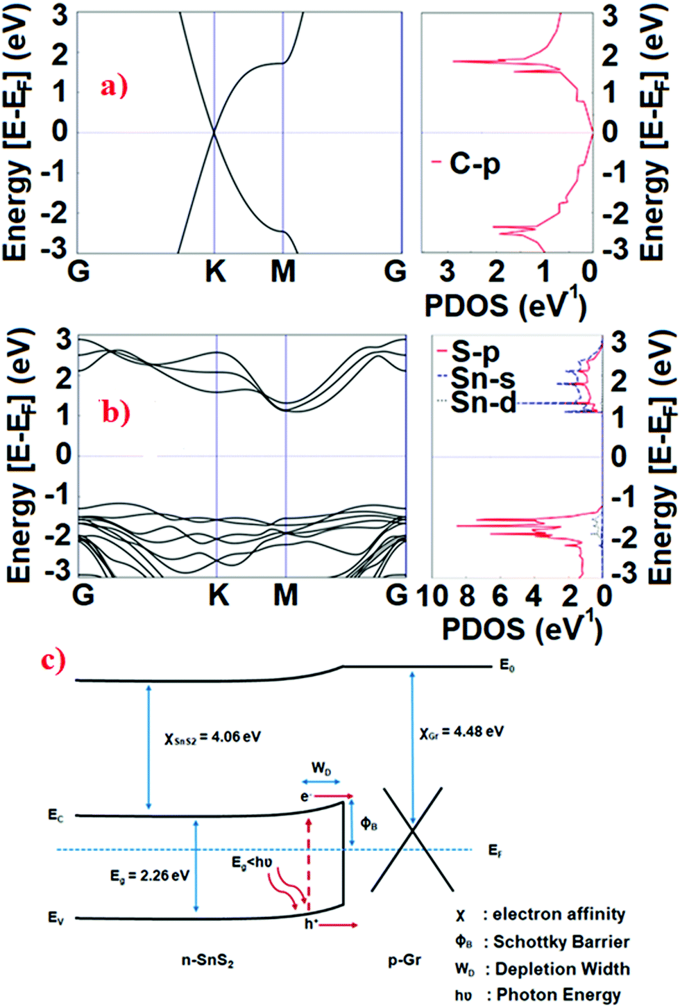 | ||
| Fig. 6 The calculated band structures and projected (orbital) electronic density of state profiles of the tri-layer: (a) Gr, (b) SnS2, and (c) band-diagram of the SnS2/Gr heterojunction. | ||
There are various reports on SnS2 based photodetectors because of their low-cost, environmental friendly nature, and excellent optoelectronic properties and the wide variety of synthesis approaches they offer.37,38 Huang et al., performed the exfoliation of the SnS2 monolayer and demonstrated it as an efficient photodetector.39 Song et al., fabricated a high performance top gate monolayer SnS2 based transistor using chemical vapor transport method for next generation flexible optoelectronic applications.40 Xiang et al., developed a process for a large area growth of SnS2 using the chemical vapour deposition technique and projected its application as a photodetector.21 Su et al., studied the dielectric screening effect and concluded that it enhances the photogenerated carrier mobility leading to higher responsivity.41 Even though there are reports on SnS2 based photodetectors, the fabrication technique involved is highly sophisticated which not only makes it expensive but also energy inefficient and not suitable for mass production. Furthermore, the use of pristine SnS2 has the issue of recombination which affects the performance of the fabricated device. Chen et al., demonstrated the use of SnS2/Gr for photodetection application.42 But SnS2/Gr was drop cast which is a very facile method and leads to device to device variation in performance. Furthermore, no detailed transport mechanism was studied to understand this unique heterostructure. To date, there are few first principles calculation based reports on Gr/SnS2 heterostructures and to the best of authors’ knowledge none of these reports explored Gr/SnS2 for photodetection application.43,44 There are no reports on utilizing the direct growth of SnS2 on a flexible substrate with high repeatability and Gr as a transport layer to enhance the photodetection performance. In this work, we demonstrate the large area growth of SnS2 on Gr/cellulose paper and its utilization as a broadband photodetector. Also, detailed DFT simulations were performed to thoroughly understand the band structure and charge transport mechanism. Furthermore, the process is generalized and can be applied to any functional material or substrate of choice. The overall cost for the fabrication of a single SnS2/Gr device was ∼0.3 $. The entire fabrication process is scalable and can also be used for large area synthesis.
Conclusion
This report is the first demonstration of large area growth of SnS2 on a Gr dip coated cellulose paper substrate and its application as an efficient broadband photodetector. Detailed DFT based first principles calculations were performed to understand the band structure and the charge transport mechanism of this unique heterojunction. The responsivity was calculated to be 6.98 and 3.67 mA W−1 for visible and UV light illumination, respectively, suggesting the device to be more responsive towards the visible region which might be attributed to the higher absorption in the visible spectrum. The fabricated device was highly durable as it was noted that there was a negligible change in the responsivity values after 500 bending cycles. The successful fabrication of such a low-cost, simple yet highly effective SnS2/Gr heterojunction on biodegradable cellulose paper opens up avenues of research on wearable broadband photodetectors.Conflicts of interest
There are no conflicts to declare.Acknowledgements
PS acknowledges the funding from SERB (SRG/2020/000098). PS acknowledges the funding from BITS Pilani (ACRG Grant). SK acknowledges the OPERA Grant from Birla Institute of Technology and Science (BITS) Pilani. The authors thank the Central Analytical Laboratory, BITS Pilani Hyderabad Campus for assistance with materials characterization.References
- L. Sang, M. Liao and M. Sumiya, A comprehensive review of semiconductor ultraviolet photodetectors: From thin film to one-dimensional nanostructures, Sensors, 2013, 13(8), 10482–10518 CrossRef CAS PubMed.
- M. Long, P. Wang, H. Fang and W. Hu, Progress, challenges, and opportunities for 2D material based photodetectors, Adv. Funct. Mater., 2019, 29(19), 1803807 CrossRef.
- L. Zeng, D. Wu, J. Jie, X. Ren, X. Hu, S. P. Lau and Y. H. Tsang, van der Waals epitaxial growth of mosaic-like 2D platinum ditelluride layers for room-temperature mid-infrared photodetection up to 10.6 μm, Adv. Mater., 2020, 32(52), 2004412 CrossRef PubMed.
- L. H. Zeng, D. Wu, S. H. Lin, C. Xie, H. Y. Yuan, W. Lu and Y. H. Tsang, Controlled synthesis of 2D palladium diselenide for sensitive photodetector applications, Adv. Funct. Mater., 2019, 29(1), 1806878 CrossRef.
- L. H. Zeng, S. H. Lin, Z. J. Li, Z. X. Zhang, T. F. Zhang, C. Xie and Y. H. Tsang, Fast, self-driven, air-stable, and broadband photodetector based on vertically aligned PtSe2/GaAs heterojunction, Adv. Funct. Mater., 2018, 28(16), 1705970 CrossRef.
- L. H. Zeng, Q. M. Chen, Z. X. Zhang, D. Wu, H. Yuan, Y. Y. Li and Y. H. Tsang, Multilayered PdSe2/perovskite Schottky junction for fast, self-powered, polarization-sensitive, broadband photodetectors, and image sensor application, Adv. Sci., 2019, 6(19), 1901134 CrossRef CAS PubMed.
- N. Huo and G. Konstantatos, Recent progress and future prospects of 2D-based photodetectors, Adv. Mater., 2018, 30(51), 1801164 CrossRef PubMed.
- H. S. Nalwa, A review of molybdenum disulfide (MoS2) based photodetectors: From ultra-broadband, self-powered to flexible devices, RSC Adv., 2020, 10(51), 30529–30602 RSC.
- D. Wu, J. Guo, J. Du, C. Xia, L. Zeng, Y. Tian and J. Jie, Highly polarization-sensitive, broadband, self-powered photodetector based on graphene/PdSe2/germanium heterojunction, ACS Nano, 2019, 13(9), 9907–9917 CrossRef CAS PubMed.
- L. Zeng, S. Lin, Z. Lou, H. Yuan, H. Long, Y. Li and Y. H. Tsang, Ultrafast and sensitive photodetector based on a PtSe2/silicon nanowire array heterojunction with a multiband spectral response from 200 to 1550 nm, NPG Asia Mater., 2018, 10(4), 352–362 CrossRef CAS.
- E. Wu, D. Wu, C. Jia, Y. Wang, H. Yuan, L. Zeng and X. Li, In situ fabrication of 2D WS2/Si type-II heterojunction for self-powered broadband photodetector with response up to mid-infrared, ACS Photon., 2019, 6(2), 565–572 CrossRef CAS.
- J. M. Gonzalez and I. I. Oleynik, Layer-dependent properties of SnS2 and SnSe2 two-dimensional materials, Phys. Rev. B, 2016, 94(12), 125443 CrossRef.
- L. A. Burton, T. J. Whittles, D. Hesp, W. M. Linhart, J. M. Skelton, B. Hou and D. J. Fermin, Electronic and optical properties of single crystal SnS2: An earth-abundant disulfide photocatalyst, J. Mater. Chem. A, 2016, 4(4), 1312–1318 RSC.
- M. Mohammadifar and S. Choi, A papertronic, on-demand and disposable biobattery: Saliva-activated electricity generation from lyophilized exoelectrogens preinoculated on paper, Adv. Mater. Technol., 2017, 2(9), 1700127 CrossRef.
- V. Selamneni, S. K. Ganeshan and P. Sahatiya, All MoS2 based 2D/0D localized unipolar heterojunctions as flexible broadband (UV-vis-NIR) photodetectors, J. Mater. Chem. C, 2020, 8(33), 11593–11602 RSC.
- V. Selamneni, N. Nerurkar and P. Sahatiya, Large area deposition of MoSe2 on paper as a flexible near-infrared photodetector, IEEE Sens. Lett., 2020, 4(5), 1–4 Search PubMed.
- C. P. Lee, K. Y. Lai, C. A. Lin, C. T. Li, K. C. Ho, C. I. Wu and J. H. He, A paper-based electrode using a Gr dot/PEDOT:PSS composite for flexible solar cells, Nano Energy, 2017, 36, 260–267 CrossRef CAS.
- Y. Lei, S. Song, W. Fan, Y. Xing and H. Zhang, Facile synthesis and assemblies of flowerlike SnS2 and In3+-doped SnS2: Hierarchical structures and their enhanced photocatalytic property, J. Phys. Chem. C, 2009, 113(4), 1280–1285 CrossRef CAS.
- S. Y. Hong, R. Popovitz-Biro, Y. Prior and R. Tenne, Synthesis of SnS2/SnS fullerene-like nanoparticles: a superlattice with polyhedral shape, J. Am. Chem. Soc., 2003, 125(34), 10470–10474 CrossRef CAS PubMed.
- Y. T. Lin, J. B. Shi, Y. C. Chen, C. J. Chen and P. F. Wu, Synthesis and characterization of tin disulfide (SnS2) nanowires, Nanoscale Res. Lett., 2009, 4(7), 694 CrossRef CAS PubMed.
- Y. Huang, H. X. Deng, K. Xu, Z. X. Wang, Q. S. Wang, F. M. Wang and J. He, Highly sensitive and fast phototransistor based on large size CVD-grown SnS2 nanosheets, Nanoscale, 2015, 7(33), 14093–14099 RSC.
- M. J. Allen, V. C. Tung and R. B. Kaner, Honeycomb carbon: A review of Gr, Chem. Rev., 2009, 110(1), 132–145 CrossRef PubMed.
- Z. Khan, N. Parveen, S. A. Ansari, S. T. Senthilkumar, S. Park, Y. Kim and H. Ko, Three-dimensional SnS2 nanopetals for hybrid sodium–air batteries, Electrochim. Acta, 2017, 257, 328–334 CrossRef CAS.
- Z. Qin, K. Xu, H. Yue, H. Wang, J. Zhang, C. Ouyang and D. Zeng, Enhanced room-temperature NH3 gas sensing by 2D SnS2 with sulfur vacancies synthesized by chemical exfoliation, Sens. Actuators, B, 2018, 262, 771–779 CrossRef CAS.
- T. Sriv, K. Kim and H. Cheong, Low-frequency Raman spectroscopy of few-layer 2H-SnS2, Sci. Rep., 2018, 8(1), 10194 CrossRef PubMed.
- R. S. Veerla, P. Sahatiya and S. Badhulika, Fabrication of a flexible UV photodetector and disposable photoresponsive uric acid sensor by direct writing of ZnO pencil on paper, J. Mater. Chem. C, 2017, 5(39), 10231–10240 RSC.
- V. Selamneni, H. Raghavan, A. Hazra and P. Sahatiya, MoS2/Paper decorated with metal nanoparticles (Au, Pt, and Pd) based plasmonic-enhanced broadband (visible-NIR) flexible photodetectors, Adv. Mater. Interfaces, 2021, 2001988 CrossRef CAS.
- P. Sahatiya and S. Badhulika, Strain-modulation-assisted enhanced broadband photodetector based on large-area, flexible, few-layered Gr/MoS2 on cellulose paper, Nanotechnology, 2017, 28(45), 455204 CrossRef PubMed.
- B. P. Yalagala, P. Sahatiya, C. S. R. Kolli, S. Khandelwal, V. Mattela and S. Badhulika, V2O5 nanosheets for flexible memristors and broadband photodetectors, ACS Appl. Nano Mater., 2019, 2(2), 937–947 CrossRef CAS.
- O. Lopez-Sanchez, D. Lembke, M. Kayci, A. Radenovic and A. Kis, Ultrasensitive photodetectors based on monolayer MoS2, Nat. Nanotechnol., 2013, 8(7), 497 CrossRef CAS PubMed.
- T. J. Octon, V. K. Nagareddy, S. Russo, M. F. Craciun and C. D. Wright, Fast high-responsivity few-layer MoTe2 photodetectors, Adv. Opt. Mater., 2016, 4(11), 1750–1754 CrossRef CAS.
- QuantumATK, Version 2018.06, Synopsys Inc., Mountain View, CA, USA, Jun. 2012. [Online]. Available: http://www.synopsys.com.
- L. Li, S. Reich and J. Robertson, Defect energies of graphite: Density-functional calculations, Phys. Rev. B: Condens. Matter Mater. Phys., 2005, 72, 184109 CrossRef.
- S.-J. Liang and L. K. Ang, Electron thermionic emission from Gr and a thermionic energy converter, Phys. Rev. Appl., 2015, 3, 014002 CrossRef CAS.
- L. A. Burton, D. Colombara, R. D. Abellon, F. C. Grozema, L. M. Peter, T. J. Savenije, G. Dennler and A. Walsh, Synthesis, characterization, and electronic structure of single-crystal SnS, Sn2S3, and SnS2, Physi. Rev. Appl., 2016, 6, 014009 CrossRef.
- X. Zhu, X. Luo, H. Yuan, H. Chen and C. Tian, Band gap engineering of SnS2 nanosheets by anion–anion codoping for visible-light photocatalysis, RSC Adv., 2018, 8, 3304 RSC.
- J. Xia, D. Zhu, L. Wang, B. Huang, X. Huang and X. M. Meng, Large-scale growth of two-dimensional SnS2 crystals driven by screw dislocations and application to photodetectors, Adv. Funct. Mater., 2015, 25(27), 4255–4261 CrossRef CAS.
- Y. Tao, X. Wu, W. Wang and J. Wang, Flexible photodetector from ultraviolet to near infrared based on a SnS2 nanosheet microsphere film, J. Mater. Chem. C, 2015, 3(6), 1347–1353 RSC.
- Y. Huang, E. Sutter, J. T. Sadowski, M. Cotlet, O. L. Monti, D. A. Racke and P. Sutter, Tin disulfide an emerging layered metal dichalcogenide semiconductor: Materials properties and device characteristics, ACS Nano, 2014, 8(10), 10743–10755 CrossRef CAS PubMed.
- H. S. Song, S. L. Li, L. Gao, Y. Xu, K. Ueno, J. Tang and K. Tsukagoshi, High-performance top-gated monolayer SnS2 field-effect transistors and their integrated logic circuits, Nanoscale, 2013, 5(20), 9666–9670 RSC.
- G. Su, V. G. Hadjiev, P. E. Loya, J. Zhang, S. Lei, S. Maharjan and H. Peng, Chemical vapor deposition of thin crystals of layered semiconductor SnS2 for fast photodetection application, Nano Lett., 2014, 15(1), 506–513 CrossRef PubMed.
- X. Chen, Z. Huang, X. Ren, G. Xu, J. Zhou, Y. Tao and J. Zhong, Photodetectors based on SnS2/Gr heterostructure on rigid and flexible substrates, ChemNanoMat, 2018, 4(4), 373–378 CrossRef CAS.
- C. S. Rout, P. D. Joshi, R. V. Kashid, D. S. Joag, M. A. More, A. J. Simbeck, M. Washington, S. K. Nayak and D. J. Late, Enhanced field emission properties of doped Gr nanosheets with layered SnS2, Appl. Phys. Lett., 2014, 105, 043109 CrossRef.
- A. Samad, M. Noor-A-Alam and Y.-H. Shin, First principles study of a SnS2/Gr heterostructure: A promising anode material for rechargeable Na ion batteries, J. Mater. Chem. A, 2016, 4, 14316 RSC.
Footnote |
| † Electronic supplementary information (ESI) available. See DOI: 10.1039/d1ma00054c |
| This journal is © The Royal Society of Chemistry 2021 |