
 Open Access Article
 This Open Access Article is licensed under a
 Creative Commons Attribution 3.0 Unported Licence
Defect tolerant device geometries for lead-halide perovskites†
Basita
Das
 *ab,
Zhifa
Liu
a,
Irene
Aguilera
a,
Uwe
Rau
ab and
Thomas
Kirchartz
*ac
*ab,
Zhifa
Liu
a,
Irene
Aguilera
a,
Uwe
Rau
ab and
Thomas
Kirchartz
*ac
aIEK5-Photovoltaik, Forschungszentrum Jülich, 52425 Jülich, Germany. E-mail: b.das@fz-juelich.de; t.kirchartz@fz-juelich.de
bFaculty of Electrical Engineering and Information Technology, RWTH Aachen University, Mies-van-der-Rohe-Straße 15, 52074 Aachen, Germany
cFaculty of Engineering and CENIDE, University of Duisburg-Essen, Carl-Benz-Str. 199, 47057 Duisburg, Germany
First published on 12th April 2021
Abstract
The term “defect tolerance” is widely used in the literature to describe materials such as lead-halides perovskites, where solution-processed polycrystalline thin films exhibit long non-radiative lifetimes of microseconds or longer. Studies on defect tolerance of materials mostly look at the properties of the host material and/or the chemical nature of defects that affect their capture coefficients. However, the recombination activity of a defect is not only a function of its capture coefficients but also depends on the electrostatics and the design of the layer stack of a photovoltaic device. Here we study the influence of device geometry on defect tolerance by combining calculations of capture coefficients with device simulations. We derive generic device design principles which can inhibit recombination inside a photovoltaic device for a given set of capture coefficients based on the idea of slowing down the slower of the two processes (electron and hole capture) even further by modifying electron and hole injection into the absorber layer. We use the material parameters and typical p–i–n device geometry representing methylammonium lead halide perovskites solar cells to illustrate the application of our generic design principles to improve specific devices.
Introduction
With the recent interest in metal-halide perovskites for photovoltaic and optoelectronic applications, the term defect tolerance1–8 has become omnipresent in the scientific literature. While it has been coined in the context of computational material screening,6 lead-halide perovskites were the first incarnation of a defect-tolerant semiconductor with an antibonding valence band that works particularly well in solar cells and light emitting diodes.5,7 One of the key reasons for this success was that solution processed polycrystalline layers of lead-halide perovskites in a wide range of stoichiometries and with varying cations and halides showed long charge carrier lifetimes,9 high luminescence quantum yields10–14 and subsequently high open-circuit voltages14–17 and efficiencies >23%18–22 if used as a solar cell. In most classical semiconductors, intrinsic point defects (vacancy, interstitial, antisites) and other complex defects from unintended impurities (e.g. C, O in Si) can form deep defects in the bulk of the film as well as at grain boundaries, surfaces, interfaces and accelerate recombination.23 The existence of these defects makes it usually quite difficult to achieve good electronic properties without investing in complicated and (usually) energy-intensive fabrication techniques such as single crystal growth and epitaxy.24 In halide perovskites, the impact of defects is less severe, because most intrinsic point defects create rather shallow energy levels25,26 making non-radiative transitions less likely than in most other semiconductors. The prevalence of shallow defects is caused by the rather uncommon antibonding valence band6 that causes most atomic orbitals to be in the conduction or valence band of the crystal. Thus, when bonds are broken (e.g. in the presence of a vacancy), the resulting orbitals are mostly inside the bands or close to the band edges25,27,28 rather than in the middle of the bandgap as is the case for most covalent semiconductors. However, the defect tolerance of halide perovskites does not imply that defects are unimportant in these materials.29,30 In contrast, non-radiative recombination via defects still reduces device performance below the values given by the Shockley–Queisser31 limit with the topic of defect passivation32–34 being central to current device optimization strategies. While the defect tolerance of a semiconductor is certainly an extremely important topic for understanding the success of lead-halide perovskites, so far there have been few attempts to discuss how the device geometry of a solar cell can affect the vulnerability of the device to defects.Whether a defect causes substantial recombination not only depends on the density and energetic position of defects but also on the availability of electrons and holes to be captured by these defects. If for instance the material has an abundance of defects that preferentially trap holes, the capture of electrons is likely the rate-limiting step. If the device geometry is then designed such that there is an excess of holes in the absorber layer of the device, electron capture would be further reduced, and the total device efficiency may go up. However, changing the properties of the device geometry has a multitude of consequences given that the device geometry has to allow efficient charge extraction, therefore provide selectivity35–37 at the different contacts, allow sufficient light absorption and efficient current flow minimizing resistive losses. Therefore, the perfect design of the device geometry under the explicit consideration of the properties of the dominant defects is a non-trivial task.
Here, we investigate the effect of device geometry on the recombination efficiency of defects, and hence on the efficiency of the solar cell. A review of well-studied materials23 like Si,38–41 GaAs,42–44 CdTe45,46 indicates that asymmetric capture coefficients are common and that its impact on recombination rates in combination with electron and hole concentration have been discussed in widely-used textbooks on the topic of recombination in semiconductors.47 However, in the field of perovskite photovoltaics, measuring capture coefficients48–50 and defect densities48–50 is highly challenging due to the variety of different relevant perovskite materials, the low defect densities, the lack of actual doping and the presence of mobile ions.51,52 Hence, for lack of better information, a near universal assumption of symmetric capture coefficients is made in studies on perovskite device simulation.53,54 However, recent calculations1,55 and fundamental arguments56 show that defects most likely have asymmetric capture coefficients; i.e. a defect is not as likely to capture an electron as a hole or vice-versa. From a device point of view, the net impact of defects can be reduced by modulating the carrier concentration inside the device such that one of the capture rates is substantially slower than the other.47 Modulating the carrier concentration by doping to minimize recombination losses is an obvious part of device optimization in technologies such as crystalline Si.57 However, in emerging technologies such as halide perovskites, where intentional doping is challenging to achieve, the topic has so far received little attention.32–34 This is despite the fact that modulation of carrier concentrations in the absorber layer is possible even without absorber-layer doping but alternatively by changing the properties of the electron and hole transport layers. Unfortunately, there is no one device geometry that will improve performance of all devices. However, the current work offers certain generic design principles which when implemented after identifying the dominant recombination levels will help reduce the recombination through the device.
This work explains how asymmetric device architectures improve open-circuit voltage of a device as seen from real device data14 by mitigating defect-mediated recombination inside the device. It also discusses the role of the built-in-voltage in controlling the carrier concentration inside the device which then directly affects the solar cell device performance.58,59 We highlight the importance of the electrostatic potential drop across the device60 and how it alters the efficiency by either enhancing or mitigating the recombination through defects. We also show that the perovskite solar cell efficiency is limited by slow charge extraction due to the low-mobility organic transport layers61 and can be improved if the low-mobility transport layers were to be replaced with higher-mobility transport layers. Besides, this work also considers the importance of atomistic calculations1,55,62–66 or generalized models56,67 in determining realistic values of capture coefficients and how these parameters can improve solar cell device simulation to help then go beyond the current state-of-the-art of symmetric capture coefficients.53,54,61
Theoretical background
Defect-mediated recombination
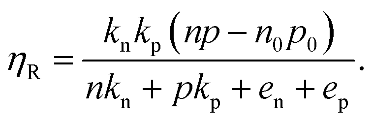
Defects occurring within the bandgap of a semiconductor enhance recombination in the device as they form an alternative recombination channel for the charge carriers besides band to band recombination. The theoretical description of this accelerated recombination via defects is based on work by Shockley, Read and Hall68,69 and is therefore known as Shockley–Read–Hall (SRH) recombination. To help understanding the results and discussion in the remainder of the article, we will briefly introduce the key terminology of SRH recombination in the following.Recombination via singly charged defects (donor-like or acceptor-like) occurs when the defect goes through a cycle consisting of two consecutive processes of electron capture and hole capture. The rate of recombination via such a defect depends on the electron capture rate (per unit time) nkn [s−1] and hole capture rate pkp [s−1], where n and p are the electron and hole concentration, and kn [cm3 s−1] and kp [cm3 s−1] are the electron and hole capture coefficient, respectively. The rate of recombination (per unit time and volume) [cm−3 s−1] is then given as
| RSRH = NTηR, | (1) |
 | (2) |
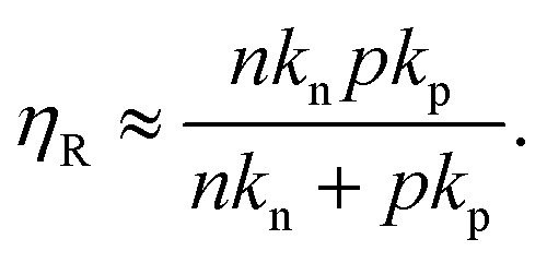
Furthermore, for defect levels lying well inside the two quasi-Fermi levels the emission coefficients are such that en ≫ nkn and ep ≫ pkp and by assuming np ≫ n0p0, the recombination efficiency can be simplified as follows
 | (3) |
Inside a device, the electron and hole carrier concentrations n0 and p0 in equilibrium, and n and p in typical operating conditions, respectively, are affected by the workfunctions and doping densities of the different layers in the device, whereas the capture coefficients kn/p are determined by the chemical nature and energetic position of a defect within the bandgap. The electron and hole emission coefficients en and ep depend on the respective capture coefficients and the position of the quasi-Fermi level splitting given by the typical operating conditions of the device.56 Recombination efficiency is therefore affected by the combined properties of the device geometry and the nature of the defects.
However, SRH statistics is agnostic about the origin of the capture coefficients and makes no theoretical prediction about the values representative of kn/p in materials. In absence of a model to predict the values of capture coefficients, state-of-the-art device simulation of perovskite solar cells uses capture coefficients obtained from experimental methods54 or heuristic assumptions70 to calculate electron hole capture lifetimes τn/p = (NTkn/p)−1. The frequently used assumption of symmetric capture coefficients kn = kp for all defect levels within the bandgap in a device operating in a high injection scenario n = p leads to a simplified picture where all defects within the two quasi-Fermi are equally recombination active. This behavior of defects is often used in textbooks for photovoltaics to illustrate the impact of capture and emission coefficients on the SRH recombination rate or recombination lifetime.71,72 However, equal or at least similar values of the capture coefficients are not necessarily a typical or even a likely scenario55,56 as has been discussed in the introduction.
To go beyond the state-of-the-art device simulation in perovskite photovoltaics involving symmetric capture coefficients, we either need more experimental data on capture coefficients of novel materials or, alternatively, models to calculate trap energy dependent capture coefficients. These can then be used in combination with SRH statistics to get a trap energy dependent recombination efficiency and SRH lifetime.
Capture coefficients
Recently we presented a generalized microscopic model,56,67 within the limits of harmonic oscillator approximation, to calculate multiphonon capture coefficients using material properties of the host semiconductor and energetic position of the trap within the bandgap of the material. The model to calculate the capture coefficients is adapted from the work of Markvart73–76 which uses the Wentzel, Kramers, Brillouin (WKB)77–79 approximation to calculate the multiphonon transition rates between two states by tunneling. The capture coefficients so calculated are proportional to the inverse of exponential of the required number of phonons for a given transition (refer to eqn (S3) for kn/p in ESI:† the argument of exponential is negative when the phonon energy is sufficiently smaller than 2kBT). However, this model does not make any predictions about the value of the Huang Rhys factor. Therefore, we combined the approach of Markvart with work of Ridley,80–82 which uses the so called ‘quantum defect model’ to calculate the Huang–Rhys factor by characterizing the defects’ degree of localization by the quantum defect parameter, νT. The parameter νT,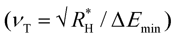 defined as the square root of the depth ΔEmin of any defect level ET from the nearest band with respect to the depth of a shallow defect given by effective Rydberg energy
  , ensures that the higher the depth of the defect, the more localized it is. The quantum defect parameter νT diminishes as the depth of the defect ΔEmin from the nearest band increases and assumes the smallest value when the defect is at midgap. The Huang–Rhys factor SHR measuring the displacement of the lattice from its mean position in the vicinity of the defect is an inverse function of νT and increases with increasing ΔEmin. Besides the type of coupling, (polar optical coupling for polar semiconductors or optical deformation potential coupling for elemental semiconductors or less polar semiconductors) also the charge state of the defect, μ, is considered in the calculation of SHR. The Huang–Rhys factor is then used to calculate the capture coefficients of defects (see Table SI in ESI† for expressions)56 in the material. The model we use therefore includes the effect of the depth of a defect twice. The depth affects the likelihood of a multiphonon transition by affecting the required number of phonons to bridge the energy gap between excited and ground state of a transition, and the use of the quantum defect model affects the transition probability by increasing the Huang–Rhys factor for more localized (i.e. deep) defects. As we show in more detail in the ESI† (see Fig. S1), the first effect (number of phonons needed for the transition) is by far the dominant one. Detailed accounts of the various models available for calculating the multiphonon capture coefficients and notes on their relations to each other, as well as their validity can be found in the work of Jaros.83 To consider the Coulomb attraction between an oppositely-charged defect state and a captured carrier, the Sommerfeld factor sa is multiplied with the electron capture coefficient kn of a donor-like defect and with the hole capture coefficients kp of an acceptor-like defect. When the trap energy dependent capture coefficients are used as inputs to the SRH theory, the energy dependence of the recombination efficiency is reflected.
It is evident from the expression of the capture coefficients given in Table SI of the ESI† that kn/p are inversely dependent on the depth ΔE of a trap via its dependence on the number of phonons. The depth ΔE of the trap is always measured with respect to the band edge from which the carrier is captured as shown in Fig. 1a. This ensures that the hole capture coefficient kp decreases rapidly as the defect level moves away from the valence band edge EV, whereas the electron capture coefficient kn decreases as the defect moves away from the conduction band edge EC, as shown in Fig. 1b. The faster than exponential decay of capture coefficients with respect to ΔE, measured from the respective bands of transition, makes kn and kp highly asymmetric except for around midgap, where the two are comparable or equal. The generalized model for capture coefficients predicts that in methylammonium lead iodide (MAPI) perovskite even defects lying within 200 meV on either side of midgap have kn and kp values differing from each other by 105 to 102 orders of magnitude as shown in Fig. 1b. This idea of asymmetric capture coefficients55 contrasts with the usual assumption of symmetric capture coefficients54,70 for any defect level and has a huge impact on the recombination efficiency of a device.
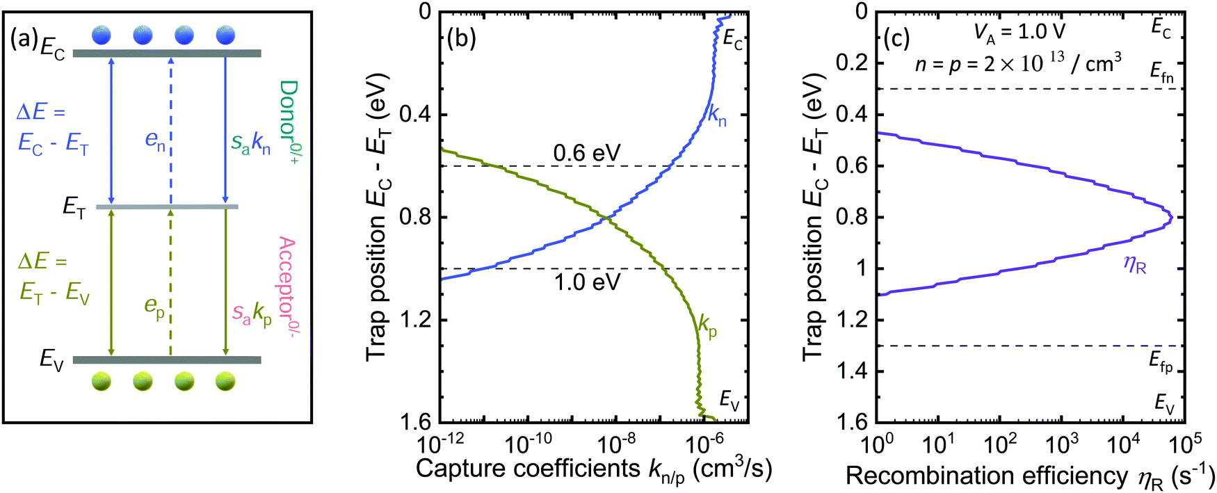 | ||
| Fig. 1 Trap energy dependent capture coefficients and recombination energy. (a) Schematic indicating the depth of trap ΔE = EC − ET for transitions taking place from conduction band or ΔE = ET − EV for transitions taking place from valence band. The electron capture coefficient kn and emission coefficient en, hole capture coefficient kp and emission coefficient ep. The kn of a donor-like trap and kp of an acceptor-like trap are multiplied with Sommerfeld factor sa to account for Coulomb interaction between oppositely charged defect state and captured carrier. (b) The capture coefficients kn/p (cm3 s−1) as functions of trap position measured from the edge of the conduction band. The capture rates are obtained by multiplying the electron and hole carrier concentration with the electron and hole capture coefficients. The carrier concentration is considered to be equal and calculated at an applied voltage VA = 1.0 V. (c) The recombination efficiency ηR (s−1) as a function of trap position EC − ET. | ||
In a simple scenario of high-level injection of carriers n = p, the capture rates nkn and pkp follow the same decaying nature of the respective coefficient with respect to ΔE measured from band edge of transition. Inserting these rates into eqn (2) leads to the result shown in Fig. 1c, where within the two quasi-Fermi level splitting, set by the applied voltage VA, ηR is given by the slower of the two rates except for midgap where the two rates are symmetric and a combination of the two rates gives ηR. In the literature, often the adjectives “deep” and “shallow” are used in the context of defects to characterize how detrimental a defect is expected to be. Defect-tolerant materials are - in this context - often defined as materials that are unlikely to form many “deep” defects. However, a deep defect is not clearly defined. It could be defined by the energetic distance to the nearest band edge, by the degree of localization (the more localized, the deeper) or by a functional argument, i.e. the more detrimental, the deeper. In this paper, we follow the third approach by using the recombination efficiency ηR giving the number of recombination events at a defect per unit time to characterize a “deep” defect.
Accordingly, a defect is classified as “deep” when the defect is most detrimental for device performance. The most detrimental situation is reached, when the defect satisfies the two criteria:
| nkn = pkp | (i) |
| nkn ≫ en and pkp ≫ ep. | (ii) |
The second criterion is valid for defects occurring inside the two quasi-Fermi level of the device. The first criterion then determines the n and p values which make the electron and hole capture rate equal and thus leading a defect to its most detrimental state. In our simple scenario of n = p the first criterion is satisfied only at midgap thus making a midgap defect the most recombination active or “deep” defect.
However, the observation that only midgap defects are “deep” is a result of equal electron and hole concentration and will change as soon as we consider asymmetric carrier concentrations inside a device. It is crucial to realize that even though the capture coefficients are intrinsic properties of the defect, the recombination activity is not. The recombination efficiency of a defect is determined by the n and p values and hence can change with the change in carrier concentration within the device. Inside a device the same defect level can vary in recombination activity depending upon its position within the device. The significance of these two criteria is that, when satisfied, it indicates an occupation probability of the defect fT ∼ 0.5, and maximum recombination efficiency for the defect. When the second criterion is still valid, but n and p values are such that nkn ≠ pkp, the recombination efficiency of the particular defect is limited by the slower of the two rates. From a device perspective, the defects satisfying the two criteria are also likely to be the most detrimental of all defect levels in the device, at that particular working condition. The energy and position dependence of ηR inside a device elucidates that not all defects are equally detrimental to device performance and whether a defect is “deep” or not is determined by the working condition of the device.
To understand the realistic impact of asymmetric capture coefficients of defects inside a device, we need to go beyond the simple scenario of n = p and use asymmetric capture coefficients obtained from our general model based on the harmonic oscillator approximation in combination with a photovoltaic device simulator to map the recombination efficiency of trap levels as a function of both trap depth ΔE and position inside the device.
Results and discussion
All photovoltaic device simulations presented here, were performed using the Advanced Semiconductor Analysis (ASA) software,84,85 an integrated opto-electronical tool developed by the Photovoltaic Materials and Devices group at TU Delft. The full list of material parameters and simulation settings used for all the results presented here can be found in Table II of the ESI.†The criteria for “deep” defects discussed in the previous section are subject to the harmonic oscillator approximation. However, within this approximation, they are also valid in situations where n ≠ p and kn ≠ kp. Thus, any defect satisfying the second criterion and having asymmetric capture coefficients can act as highly recombination active site when nkn = pkp. In Fig. 2, we use the capture coefficients calculated in Fig. 1b using the harmonic approximation for MAPI to map the recombination efficiency as a function of n/p and kn/kp. The key insights we gain are:
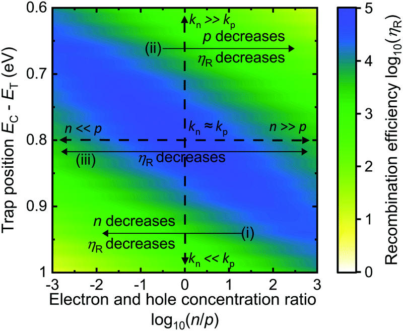 | ||
| Fig. 2 The variation of recombination efficiency ηR as function of realtive values of electron and hole concentration (n/p) and realtive values of electron and hole capture coefficients kn and kp, respectively, with the change in energetic position of the traps. Recombination efficiency decreases when the slower of the two capture rates decreases in magnitude. For a particualar defect level with fixed capture coefficients this is determined by the carrier densities. (i) When the defect is below the midgap level and closer to the valence band, ηR decreases from right to left with decrease of n with respect to p. (ii) When the defect is above the midgap level and close to the conduction band, the trend is reversed and ηR decreases from left to right with decrease of p with respect to n. (iii) The closer the defect is to midgap level, the more symmetric are coefficients and ηR decreases on either decreasing n compared to p or p compared to n. | ||
(i) The further below the defect is from midgap, the higher the electron concentration should be to obtain nkn = pkp. Alternatively, when a defect is more likely to capture a hole, kn ≪ kp; the lower the electron concentration n is compared to the hole concentration p (n ≪ p), the lower the recombination efficiency ηR will be.
(ii) The more the defect is above midgap, the higher the hole concentration should be to obtain nkn = pkp. Alternatively, when a defect is more likely to capture an electron, kn ≫ kp; the lower the hole concentration p is compared to the electron concentration n (n ≫ p), the lower the recombination efficiency ηR will be.
(iii) The closer the defect is to midgap, the more comparable the carrier concentration should be to obtain nkn = pkp. Alternatively, when a defect is equally likely to capture a hole or an electron, kn ≈ kp; either n ≫ p or n ≪ p will lead to a lower recombination efficiency ηR.
Hence, while dealing with asymmetric capture coefficients, it is better to have asymmetric carrier concentrations, which keeps the rates of capture vastly different from each other and prevents the situation of nkn = pkp.
The insights gained so far are general and can act as guidelines to investigate different device geometries of different materials. A particularly interesting test-case to study is the class of lead-halide perovskite solar cells. Here, the absorber is fairly intrinsic and the ratio n/p throughout the absorber depends to a large degree on properties of the electron and hole transport layers. For instance, the low permittivity of organic electron or hole transport layers, may cause a large drop of the electrostatic potential over the transport layers causing a smaller drop of electrostatic potential over the absorber layer. While this has been noted in the literature, so far, the impact of device electrostatics on recombination rates has not been discussed in much detail.
A perovskite solar cell (PSC) typically consists of an active layer sandwiched between an electron transport layer (ETL) and a hole transport layers (HTL) before the cathode and anode layer, respectively. In an ideal scenario, the ETL transports the electrons from the device to the cathode while blocking the holes and the HTL transports the holes from the active layer to the anode while blocking the electrons. As a result of the selectivity achieved by employing materials with different electron affinity, the difference of the workfunctions of the anode and cathode leads to a built-in-voltage Vbi across the device. At an optimum working condition, the electrostatic potential drop across the device is the net difference between the built-in-voltage Vbi and the applied voltage VA and the electrostatic potential then determines the electron and hole concentration inside the device.
We employ a device structure, with a perovskite absorber layer of 300 nm sandwiched between two generic charge transport layers each of 20 nm thickness as shown in Fig. 3. The ETL and HTL are symmetric differing only in their value of electron affinity EA. The HTL/perovskite and ETL/perovskite interfaces are modelled by two additional layers each of 2 nm and characterized by material parameters of the absorber layer. However, the bandgap of this interface layer is given by a combination of the bandgap and the electron affinity of the two materials forming the interface as shown in Fig. 3. We also assume a constant trap density NT = 1015 cm−3 across the absorber and interface layers (see Table II in ESI† for material parameters). We then perform certain thought experiments realizing different n/p ratios through our generic device by changing the electrostatic potential drop across the absorber and the contacts to correlate those variations in the ratio n(x)/p(x) to the efficiency of the solar cell.
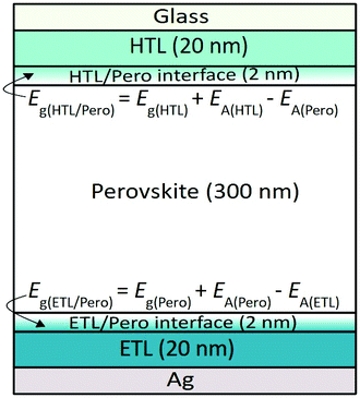 | ||
| Fig. 3 p–i–n device structure of the perovskite solar cell under study. The generic hole transport layer (HTL) and electron transport layer (ETL) are symmetric differing only in their electron affinity (EA). The interface layers are characterized by parameters of the absorber except for their bandgaps are given according to expressions shown in the figure. | ||
Symmetric device with varying built-in-voltage:
The built-in-potential is determined by the energetic mismatch between the workfunctions of the anode and the cathode. When the Schottky barrier height at both the contacts are zero, the built-in-potential is equal to the bandgap of the absorber. When the workfunctions of both the metal contacts are such that there is a non-zero Schottky barrier at the ETL side and as well as the HTL side, then the built-in-potential is qVbi = Eg(abs) − ξp − ξn, where ξp and ξn are the Schottky barrier heights at the HTL/anode interface and the ETL/cathode interface, respectively. We consider two scenarios such that in one ξp = ξn = 0 eV; qVbi = 1.6 eV and in another ξp = ξn = 0.2 eV; qVbi = 1.2 eV. In our symmetric device, the hole concentration p and the electron concentration n vary such that p ≫ n towards the HTL side and n ≫ p towards the ETL side leading to a continuously varying n/p ratio inside the device.In Fig. 4a and b we plotted the band diagram of the two devices and then superimposed on it the logarithm of the absolute value of recombination efficiency ηR as a function of both the position inside the device and the position of the defect as measured from the conduction band edge. To explain the effect of the change in qVbi on the recombination efficiency we also plot the electron and hole concentration through the device at qVbi = 1.6 eV (solid blue curves) and at qVbi = 1.2 eV (dashed pink curve) in Fig. 4c. When qVbi = 1.6 eV, the hole to electron concentration ratio varies in range p/n ≈ 104 to 10−4 from the HTL side to the ETL side as shown in Fig. 4c. This suggests that any defect that has kn/kp ≈ 104 has the potential to act as a “deep” defect at the HTL side and so does a defect with kn/kp ≈ 10−4 at the ETL side by satisfying the condition nkn = pkp. In case of MAPI, as plotted in Fig. 1b, one such defect is about 0.6 eV from the conduction band with kn/kp ≈ 104 whereas another one is about 1.0 eV away from the conduction band with kn/kp ≈ 10−4. Hence these two defects even with highly asymmetric capture coefficients satisfy the “deep” defect criteria of nkn = pkp in different regions of the device. As we go inside the device from the HTL side the hole to electron concentration ratio decreases such that 104 > p/n > 10−4. This implies that as we move inside the device from the HTL side to the ETL side, any defect within 200 meV on either side of midgap, having capture coefficients such that 104 > kn/kp > 10−4, can potentially be turned into a “deep” defect or at least highly recombination active defect when the criteria kn/kp ≈ p/n is satisfied at a position inside the device. This highly recombination active region appears in the shade of blue in Fig. 4a and ηR peaks around midgap at an approximate value of 105 s−1.
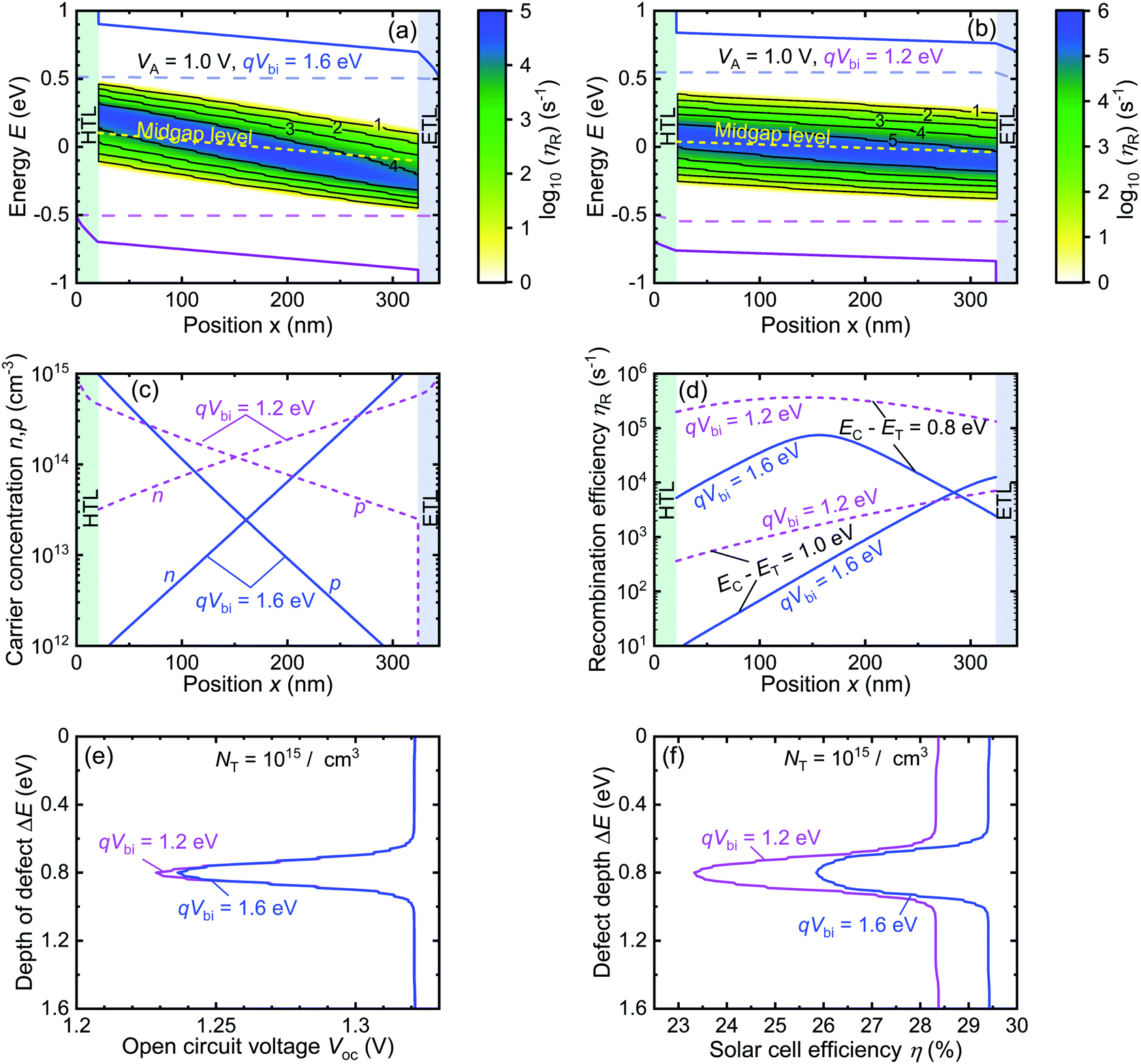 | ||
| Fig. 4 The effect of changing the built-in-voltage Vbi across the device on SRH recombination and subsequently on the device efficiency. (a) Recombination efficiency ηR as a function of position inside a device and the energy level (EC − ET) of the trap calculated from the conduction band when qVbi = 1.6 eV. This data is superimposed on the band diagram of the device at an applied voltage VA = 1.0 V. (b) Same as before but for qVbi = 1.2 eV. (c) The electron and hole concentration inside the device when qVbi = 1.6 eV and qVbi = 1.2 eV. (d) The SRH recombination rate RSRH of defects 1.0 eV and 0.8 eV away from the conduction band for qVbi = 1.6 eV and qVbi = 1.2 eV. (e) Open circuit voltage Voc plotted as a function of the position of the defect from the conduction band for qVbi = 1.6 eV and qVbi = 1.2 eV. (f) Solar cell efficiency η(%) plotted as a function of the position of the defect from the conduction band for qVbi = 1.6 eV and qVbi = 1.2 eV. | ||
In comparison to qVbi = 1.6 eV, when non-zero Schottky barriers are introduced, the electron quasi-Fermi level move ξn energy away from the conduction band at the ETL/metal interface and the hole quasi-Fermi level moves ξp away from the valence band at the HTL/metal interface. This leads to reduction of the electron concentration towards the ETL and hole concentration towards the HTL. However, the change in qVbi increases carrier concentration everywhere else inside the device as well as the minority carrier concentration towards the selective contacts (holes towards ETL and electrons towards HTL). The change in both absolute value as well as relative value of electron and hole concentration has two effects on the recombination activity of the device.
In Fig. 4c, when qVbi = 1.2 eV, the carrier concentration varies such as p/n ≈ 10 to 10−1 from the HTL side to the ETL side, which implies that only defects with coefficients such that kn/kp ≈ 10 to 10−1 are potential “deep” defects or the most detrimental of all the defects inside the device. Thus, according to the coefficients determined from harmonic oscillator approximation for MAPI (see Fig. 1b), defects within a 50 meV energy range on either side of midgap can be turned into “deep” defects by the electron and hole concentration at a particular position inside the device when qVbi = 1.2 eV. The narrowing down of the range of “deep” defects on reducing the built-in-voltage is related to the change of the relative values of electron and hole concentration inside the device. However, even though the range of “deep” defects narrowed down, comparing Fig. 4a and b reveals that the recombination efficiency of all defects increased and ηR ≈ 106 s−1 around midgap due to increase in the absolute values electron and hole concentration as shown in Fig. 4c. As a result of reducing the built-in-voltage, the recombination efficiency of below midgap defects (kn ≪ kp) at every position inside the device increases by the amount of increase in electron concentration. The same is true for defects above midgap (kn ≫ kp) but in this case, the increase in recombination efficiency is determined by the increase in the value of hole concentration.
In Fig. 4d we show the effect of the change qVbi and hence carrier concentration more explicitly by choosing to look at the recombination efficiency for two specific defect levels in MAPI with capture coefficients determined from the harmonic oscillator approximation. The defect level 1.0 eV away from the conduction band has asymmetric capture coefficients (kn ≈ 10−11 cm3 s−1 and kp ≈ 10−7 cm3 s−1) and the one 0.8 eV away from the conduction band has symmetric capture coefficients(kn ≈ kp ≈ 5 × 10⁻⁹ cm3 s−1). Both defect levels have a constant defect density of NT = 1015 cm-3 across the active and the interfaces layers. The increase in electron concentration n upon decreasing qVbi increased the rate of electron capture and hence ηR of the defect 1.0 eV away from midgap through most of the device. However, the case of the defect at midgap with symmetric values of capture coefficient is a bit more complicated. When qVbi = 1.6 eV, n and p are vastly different, making the electron and hole capture rates very different even though the coefficients are symmetric and thus ηR is determined by the slower of the two rates through most of the device. On the contrary, when qVbi = 1.2 eV, the comparable n and p values yield very similar electron and hole capture rates having higher values compared to the capture rates at qVbi = 1.6 eV and thus, ηR is determined by a combination of both capture rates.
In Fig. 4e and f we show the overall effect of the change in built-in-voltage on the open-circuit voltage Voc and efficiency of the device η (%). When the SRH recombination rate exceeds the direct recombination rate RSRH > Rdirect, Voc and efficiency η (%) decrease from their respective values given by the radiative limit. In the two devices discussed above this criterion is satisfied both by defects at midgap with symmetric coefficients and defects away from midgap with asymmetric capture coefficients. This deviation from the radiative limit within 200 meV on either side of midgap results in a drop of Voc and η (%) in this range. The drop in the values of Voc and η (%) is higher when qVbi = 1.2 eV compared to when qVbi = 1.6 eV because of the higher RSRH in the low qVbi case. Even though the range of “deep” defects shrunk with the decrease in qVbi, the actual overall recombination increased through the device due to the increase in the electron and hole concentration through the device. It should be noted that even beyond the 200 meV range on either side of midgap the non radiative recombination rate RSRH increases substantially due to the increase in carrier concentration inside the absorber when qVbi decreases from 1.6 eV to 1.2 eV, and the increased non-radiative recombination also leads to the drop in the solar cell efficiency η (%) beyond the 200 meV range on either side of midgap.
Thus, it is evident from the discussion above, that a built-in-voltage that helps in achieving relatively lower values of n and p inside the device also leads to relatively lower magnitudes of defect-mediated recombination as well as direct recombination. The rule is that if changing the built-in-potential qVbi leads to the decrease in even one of the carrier concentrations, then the capture rate of that carrier by all defect levels will also decrease. And if the capture rate that decreases due to decrease in carrier is the recombination limiting rate, then the recombination efficiency of the defect levels will decrease and as a result the efficiency of the device would increase. The results discussed above were for defect levels in the bulk. Devices limited by surface recombination are a bit more involved but show similar trends as shown in Fig. S2 and S3 of the ESI.† Also, the effect of surface recombination on device performance is shown in Fig. S4 (ESI†). Nevertheless, it is obvious that it is better to have vastly different electron and hole concentration inside the device so that the recombination rate can be slowed down by inhibiting one of the capture processes. However, even when qVbi is high, defects within 200 meV on either side of midgap act as deep defects. This will be particularly severe from a device perspective if a device has higher concentrations of defects around midgap since this will result in very high levels of defect mediated recombination. Also, in the cases we studied, due to continuously varying electron and hole concentration, the recombination efficiency of every defect level varies continuously inside the device and so does the position of “deep” defects both in energy and position inside the device. To circumvent such scenarios, we study a device geometry such that n ≪ p or p ≪ n throughout the device.
Asymmetric devices
To test our hypothesis about asymmetric carrier concentrations throughout the device we chose a device architecture with flat bands across the absorber layer by assuming absorber permittivity εpero →∞. Such a device with symmetric ETL and HTL layer gives n = p across the absorber and the interface layers and is expected to be highly detrimental for devices with defects at or around midgap. However, the recombination activity of defects close to midgap can be improved if we dope one of the contact layers as it would result in n ≫ p or p ≫ n across the absorber depending on whether we dope the ETL layer with donor dopants or the HTL layer with acceptor dopants, respectively. If we want to induce an asymmetry of electron and hole concentrations in an intrinsic semiconductor by choosing asymmetric properties of contacts, we have to rely on the contacts being able to connect the majority carrier quasi-Fermi level at the contact with the one at the edge of the absorber without any substantial gradient in quasi-Fermi level. This requires either low thicknesses or sufficiently high mobilities in the undoped electron or hole transport layer. Because this cannot be taken for granted, we will first discuss the scenario where the contact layer mobilities are sufficiently high to minimize any voltage drops. In a second step, we discuss the opposite scenario where these mobilities are low enough to cause a substantial voltage drop.In Fig. 5a and b, we plot the logarithm of the absolute value of recombination efficiency of a symmetric and asymmetric flat-band device, respectively, superimposed on the band diagram of the respective device. In the symmetric device, the electron and hole carrier concentrations are equal and constant n = p (as indicated by the position of the two quasi-Fermi level from their respective bands) between the two interface layers, resulting in the recombination efficiency peaking around midgap and decreasing rapidly beyond, as shown by the blue shaded region of Fig. 5a. In the asymmetric device shown in Fig. 5b, the ETL layer has a donor dopant concentration of Nd(ETL) = NC(ETL) and results in n ≫ p between the two interfaces. This asymmetric carrier concentration leads to reduced recombination efficiency for all defects above midgap and within 100 meV below midgap, while increasing the same for defects which are about 100–300 meV below midgap. This is so because at midgap where kn ≈ kp, n ≫ p makes nkn ≫ pkp and as a result ηR is limited by the slower hole capture rate pkp and, thus, the defects around midgap do not anymore satisfy the “deep” defect criterion of nkn = pkp. However, the “deep” defect criterion is now satisfied by defects which have capture coefficients such that kn/kp ≈ p/n, which in this case are defects situated about 100–300 meV below midgap.
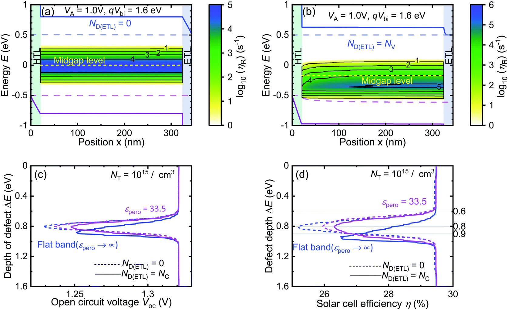 | ||
| Fig. 5 The Effect of constant but asymmetric electron and hole concentration inside a device with μpero = 30 cm2 V−1 s−1 and μETL/HTL = 10 cm2 V−1 s−1 on solar cell efficiency. (a) Defect mediated recombination efficiency ηR (s−1) as a function of position inside the device and the energy level (EC − ET) of the trap calculated for a flat-band device with symmetric ETL and HTL layer such that n = p and is superimposed on the band diagram of the same device. (b) Same as before except now the ETL layer is doped at a donor concentration of Nd(ETL) = NC. (c) Comparison of open circuit voltage Voc of devices with absorber permittivity εpero = 33.5 (purple curves) and εpero → ∞ (blue curves). The devices with symmetric (undoped) ETL/HTL are shown by dashed curves and the devices with asymmetric (doped ETL, Nd(ETL) = NC(ETL)) are represented by solid curves. (d) Solar cell efficiency of the same four devices mentioned in panel (c) is compared. | ||
In Fig. 5c and d we compare Voc and η (%) of the two flat-band devices. Also, to put their performance in perspective with that of device geometries discussed in Fig. 4, we chose two devices having contact layer mobility μETL/HTL = 10 cm2 V−1 s−1 and absorber layer permittivity εpero = 33.5. The choice of permittivity makes sure that the electron and hole concentrations vary continuously through the device. One of the two devices with εpero = 33.5 have symmetric contacts, i.e. undoped ETL or HTL (dashed purple curve) while the ETL of the other device is doped with a donor concentration of Nd(ETL) = NC(ETL)(solid purple curve). It is observed by comparison of the solid and dashed purple curves in both panels (c) and (d) that asymmetric contacts resulting in more asymmetric carrier concentration improve the Voc and η (%) of midgap defects even when the n and p vary continuously inside the device. However, making the geometry such that n ≫ p across the device inhibits the recombination of midgap defects even further. At midgap the maximum Voc and η (%) are given by the solid blue curves in Fig. 5c and d, respectively. The dashed blue curves in the same figures, representing the flat band symmetric ETL and HTL resulting in n = p throughout the absorber layer, intdicates the worst Voc and η (%) at midgap. The reference lines in Fig. 5d at 0.6 eV, 0.8 eV and 0.9 eV away from the conduction band show that within 200 meV above midgap and 100 meV below midgap, the solar cell efficiency η (%) improves as a function of the asymmetry between the electron and hole concentration inside the device.
However, even though n ≫ p helped reduce recombination through defects around and above midgap, it increases the recombination through defects 100–300 meV below midgap where kn ≪ kp. In a device where most defects are positioned such that kn ≪ kp, the HTL layer must be acceptor doped so that the electron concentration in the device remains small (n ≪ p), thus decreasing the electron capture rate nkn < pkp. Therefore, the way to deal with asymmetric capture coefficients is to have asymmetric carrier concentration inside the device so that one of the capture rates is substantially slower than the other and nkn ≠ pkp. However, to determine which geometry would improve the device efficiency, it is important to identify the dominant defect levels responsible for majority of the non-radiative recombination in the device by corroborating experimental data with first-principle studies of capture coefficients. The knowledge of the capture coefficients of the dominant defect levels can then be used to choose the appropriate scheme of asymmetry in the device that successfully reduces the recombination efficiency of the dominant defect levels. In the following section we put this idea into practice and validate our hypothesis against real device data.
Recombination through iodine interstitials
Liu et al.14 reported an open circuit voltage exceeding 1.26 V for inverted planar MAPI solar cells by carefully optimizing the hole transport layer and electron transport layer to an asymmetric champion device. In MAPI structures, iodine interstitial defects have been long suspected to be the dominant defect level4 and Zhang et al.55 calculated the capture coefficients of iodine interstitial defects from first principles. Therefore, let us assume that iodine interstitials are the dominant defect in MAPI and use the capture coefficients calculated in Zhang et al. Under these two assumptions we are able to make predictions on how the device geometry should affect device performance. We therefore simulate MAPI devices with an iodine interstitial defect level and varying asymmetries in the device geometry that modulate the relative efficiency of electron and hole injection.We fabricated a MAPI solar cell of p–i–n structure with organic charge extraction layers poly(triarylamine) (PTAA) as the hole transport layer (p) and [6,6]-phenyl-C61-butyric acid methyl ester (PCBM) as the electron transport layer (n). The PTAA layer thickness is ∼16 nm whereas the PCBM thickness is varied as ∼14 nm, 32 nm, 45 nm, and 60 nm. The current voltage curves are measured on a class AAA solar simulator providing a power density of 100 mW cm−2. The Voc increases with increase in PCBM thickness due to suppression of recombination at interfaces and in the bulk leading to an improvement in Voc as well as the efficiency as shown in Fig. 6.
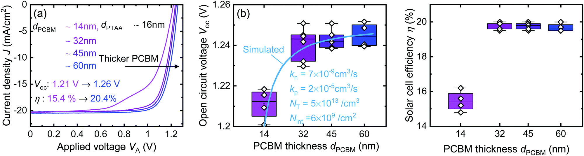 | ||
| Fig. 6 (a) Experimental J–V characteristics of inhouse fabricated standard MAPI cells showing the increase of open circuit voltage Voc with the thickness of the ETL. (b) Statistical data of open circuit voltage. The white diamonds represent experimentally observed values of Voc from which the statistical analysis is drawn. Each box represents results from three batches of cells made with the same processing parameters. All processing parameters are the same for all samples except for concentration of the solution used for the PCBM deposition. The light blue line shows the dependence of Voc on ETL thickness as observed from simulation with the trap density chosen to obtain the best fit to experimental data. (c) Statistical data of solar cell efficiency. | ||
Recently Zhang et al.55 performed first-principles calculations to determine the electron and hole capture coefficients of iodine interstitial defects about 0.48 eV away from the conduction band occurring in methylammonium lead iodide perovskite structures. Even though the iodine interstitial defect is energetically closer to the conduction band, they found the electron capture rate to be substantially slower as compared to the hole capture rate. The slowing down of the electron capture results from the strong anharmonicity in the potential energy surface of the system consisting of a positively charged iodine interstitial Ii+, an e− at the conduction band minimum (CBM) and a h+ at the valence band maximum (VBM) as shown in Fig. 7. From a semiclassical perspective, this anharmonicity results in an energetic barrier ΔEn+ between the potential energy surface (PES) of the two systems (Ii+ + e− + h+ and I0i + h+) which an electron needs to overcome to transition from the CBM (green curve) to the defect level (orange curve). On the contrary, the electron “sees” no such barrier while transitioning from the defect level to the VBM (blue curve), thus making the hole capture rate substantially faster. To study the combined effects of asymmetric geometry and the asymmetric capture coefficients of an iodine interstitial defect on perovskite solar cell performance, we take kn = 7 × 10⁻⁹ cm3 s−1 and kp = 2 × 10⁻⁵ cm3 s−1 as reported by Zhang et al.55 from first-principles calculations and simulate a symmetric and an asymmetric device for comparison.
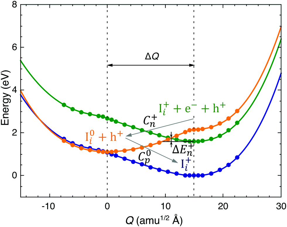 | ||
| Fig. 7 The figure shows the potential energy surfaces for charge state transitions as a function of a generalized configuration coordinate. The green curve shows the potential energy surface of a system with an electron (e−) at the conduction band minimum, a hole (h+) at the valence band maximum and an iodine interstitial defect in its unoccupied state Ii+. The Ii+ defect captures an e− from the conduction band and transitions to the I0i state represented by the orange curve. Semi-classically the process of transition from Ii+ → I0i needs to overcome a potential barrier of ΔEn+ as determined by the intersection of the potential energy surfaces (green and orange curves) of the two charge states. The defect I0i then captures a hole from the valence band and relaxes the system back to Ii+ represented by the blue curve. The small barrier of ΔEn+ resulting from the strong anharmonicity of the potential energy surface of Ii+ makes the electron capture process slower in comparison to the hole capture process as there is no such barrier between the orange and the blue curve. Reprinted figure with permission35 from Xie Zhang et al., Phys. Rev. B101, 140101(R) ©2020, American Physical Society. (https://doi.org/10.1103/PhysRevB.101.140101). | ||
In Fig. 8a and b, we plot the band diagram of the symmetric and the asymmetric device, respectively, along with the iodine interstitial defect level 0.48 eV away from the conduction band. In the symmetric device, both the transport layers are identical with thickness dHTL,ETL = 20 nm with μHTL,ETL = 10−2 cm2 V−1 s−1, whereas in the asymmetric device the ETL has a thickness of dETL = 50 nm, and HTL thickness is dHTL = 20 nm with the mobility remaining same as before. As a result of this asymmetry, the electrostatic potential drop across the ETL increases and that across the absorber layer and the HTL decreases. The decrease in the potential drop in the absorber layer results in reduced electron concentrations inside the absorber and thus to maintain charge neutrality the hole concentrations in the absorber layer increases as shown in Fig. 8c. Now since the iodine interstitial defect has kn ≪ kp, the smaller the electron concentration n is compared to the hole concentration p, the better it is for the device as it makes nkn ≪ pkp. This is shown in Fig. 8d where a comparison of the solid blue curve and dashed purple curve reveals that the electron capture rate nkn, which is the recombination limiting rate in this case, decreases with the introduction of the asymmetry. Even though the hole capture rate increases with increasing hole concentration, the “deep” defect criterion nkn = pkp is completely avoided inside the asymmetric device. The recombination efficiency of the defect level in the asymmetric device represented by the purple open symbols also decreases and is entirely determined by the electron capture rate nkn. In Fig. 8e we obtain the non-radiative recombination rate RSRH through the iodine interstitial defect level for a defect density of NT = 1015 cm−3 across the interfaces and the absorber, and we see a substantial decrease in the amount of non-radiative recombination. The reduced non-radiative recombination leads to an improvement in performance of the PSC as corroborated by the increase of Voc by approximately 100 meV and device efficiency η (%) by more than 4.7% as shown in Fig. 8f. Fig. 8f reproduces the same trend of increase in Voc with ETL thickness as studied from the experimental results in Fig. 6.
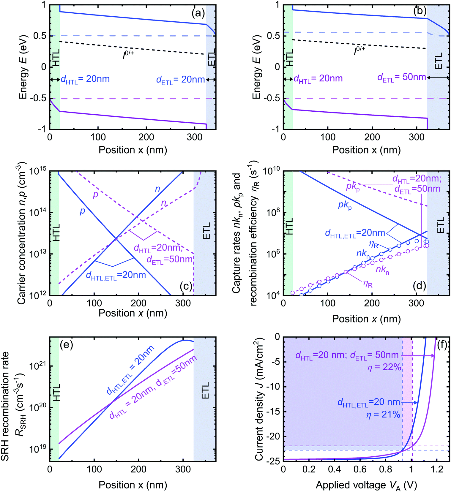 | ||
| Fig. 8 Comparison of a symmetric and an asymmetric device with an iodine interstitial defect level. (a) The band diagram of the symmetric device with dHTL,ETL = 20 nm along with the iodine interstitial defect level 0.48 eV from the conduction band. (b) The same but for the asymmetric device which has dHTL = 20 nm and dETL = 50 nm. (c) The electron concentration n and hole concentration p through the symmetric is represented by the curves in blue and that through the asymmetric device is represented in purple. (d) The electron and hole capture rates nkn and pkp of the symmetric device is shown by the solid blue curves, and that of the asymmetric device are shown by the dashed purple curves. The respective recombination efficiency ηR are shown by the open symbols. (e) The Shockley–Read–Hall recombination rate RSRH for a defect density of NT = 1015 cm−3 across the absorber and the interfaces for the symmetric (blue curve) and the asymmetric device (purple curve). (f) The J–V curve for the symmetric (blue curve) and the asymmetric device (purple curve). | ||
We used the same set of capture coefficients (kn = 7 × 10⁻⁹ cm3 s−1 and kp = 2 × 10⁻⁵ cm3 s−1) and assumed a field free absorber to mimic the screening of the electric field by mobile ions in perovskite solar cells to reproduce the trend of experimentally observed Voc as a function of PCBM thickness. We obtained the best fit (light blue line in Fig. 6b) between the experimentally observed Voc and simulated Voc for a combination of absorber defect density of NT = 5 × 1013 cm−3 and an interface defect density of Nint = 6 × 109 cm−2 at both interfaces. This correspond to an electron lifetime of τn ≈ 2 μs in the absorber and a surface recombination velocity Sn = 42 cm s−1 for electrons, where Sn is analytically defined as Sn = Nint × kn. The electron capture coefficient being much smaller compared to the hole capture coefficient, the electron capture acts as the rate limiting step at open circuit. However, even though we reproduce the increase in Voc with PCBM thickness due to reduced defect mediated recombination, this is not evidence that the asymmetric capture coefficients have to be the only or the major cause of this trend. Additional effects such as e.g. better coverage of rough perovskite surfaces may be superimposed, whose effects we would not be able to disentangle from the effects of asymmetric capture coefficients.
Effect of the transport layer mobility on the device efficiency
The carrier selective transport layers (TLs) on either side of the perovskite absorber layer are responsible for the transport of the photogenerated charge carriers from the absorber layer to the extracting electrodes. However, the organic TL suffer from low mobilities such that μHTL,ETL ≈ 10−5–10−2 cm2 V−1 s−1,![[thin space (1/6-em)]](https://www.rsc.org/images/entities/char_2009.gif) 86,87 which is orders of magnitude lower than the mobility exhibited by the perovskite layer μpero ≈ 1–10 cm2 V−1 s−1.88 These low mobilities of the state-of-the-art transport layers act as an efficiency limiting factor for PSCs.87 To investigate this relationship between TL mobility and device efficiency we choose to look at both symmetric as well as asymmetric perovskite device structures with a single defect level given by the iodine interstitial defect as was used in the previous section. In Fig. 9a to d we plot the band diagrams of four different device geometries at three different values of TL mobilities such that μHTL,ETL = [10−5 cm2 V−1 s−1, 10−2 cm2 V−1 s−1, 10 cm2 V−1 s−1] to show the position of the quasi-Fermi level as a function of the transport layer mobilities.
86,87 which is orders of magnitude lower than the mobility exhibited by the perovskite layer μpero ≈ 1–10 cm2 V−1 s−1.88 These low mobilities of the state-of-the-art transport layers act as an efficiency limiting factor for PSCs.87 To investigate this relationship between TL mobility and device efficiency we choose to look at both symmetric as well as asymmetric perovskite device structures with a single defect level given by the iodine interstitial defect as was used in the previous section. In Fig. 9a to d we plot the band diagrams of four different device geometries at three different values of TL mobilities such that μHTL,ETL = [10−5 cm2 V−1 s−1, 10−2 cm2 V−1 s−1, 10 cm2 V−1 s−1] to show the position of the quasi-Fermi level as a function of the transport layer mobilities.
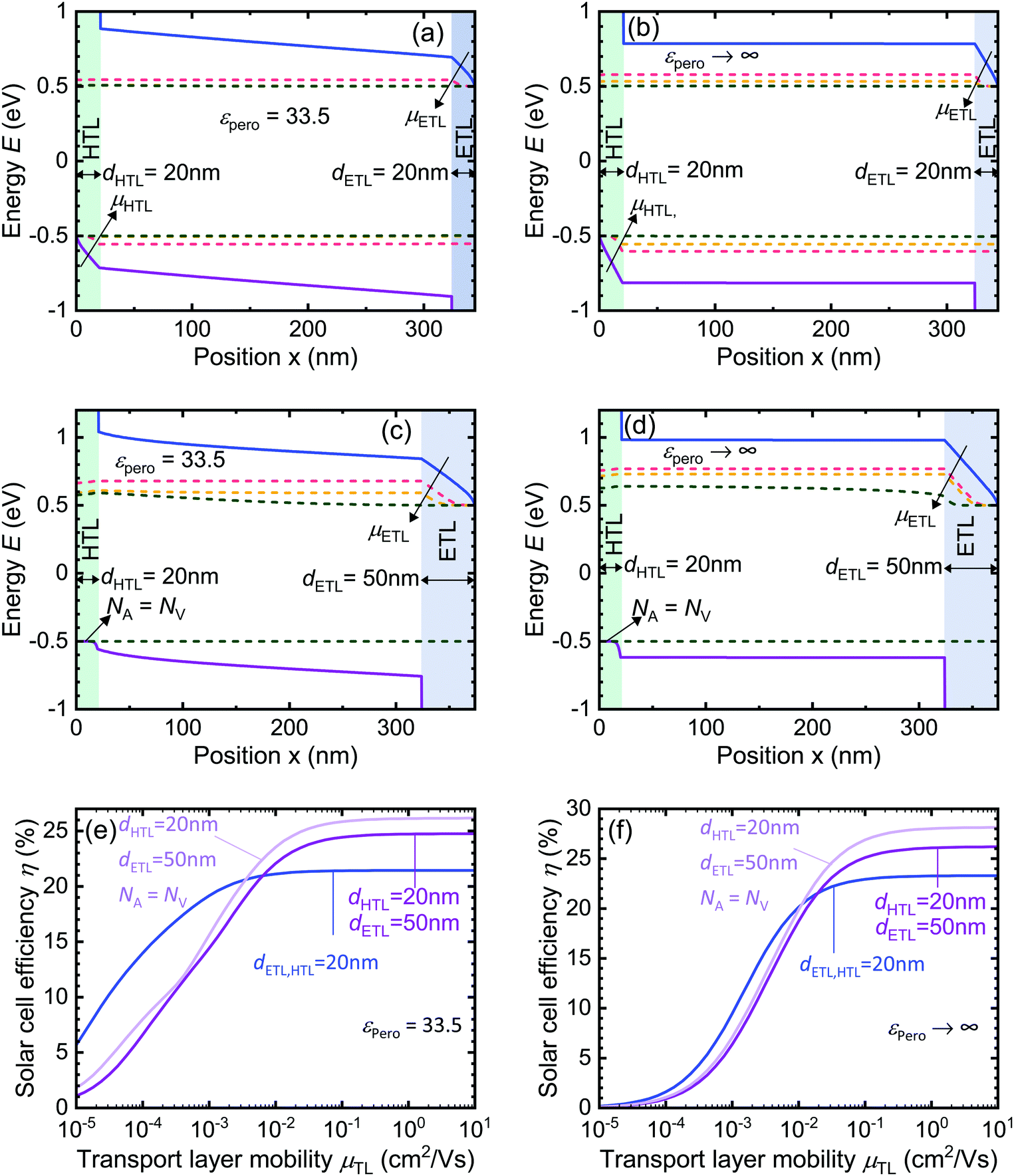 | ||
| Fig. 9 Effect of transport layer mobility on the efficiency of the device. (a) Band diagram of a symmetric device with εpero → 33.5,dHTL,ETL = 20 nm and with one defect level at 0.48 eV away from the conduction band at three different values of transport layer mobility μHTL,ETL = [10−5 cm2 V−1 s−1, 10−2 cm2 V−1 s−1, 10 cm2 V−1 s−1]. (b) Same as in (a) but now the permittivity of the absorber εpero → ∞. (c) Band diagram of an asymmetric device with εpero → 33.5, dETL = 50 nm, dHTL = 20 nm, acceptor doped HTL layer and with one defect level at 0.48 eV away from the conduction band at three different values of transport layer mobility as before. (d) Same as in (c) but now the permittivity of the absorber εpero → ∞. (e) The efficiency η (%) of the different solar cell geometries with εpero → 33.5 as a function of transport layer mobility. (f) Same as in (e) but for solar cell geometries with εpero → ∞. | ||
In Fig. 9a and b, we show the band diagrams of the undoped device geometries as for εpero = 33.5 and εpero → ∞, respectively. As we increase the TL mobility from 10−5 cm2 V−1 s−1 to 10 cm2 V−1 s−1, the electron quasi-Fermi level (Efn) and hole quasi-Fermi level (Efp) do not bend along the curvature of the ETL conduction band and HTL valence band, respectively. At high mobilities due to faster charge extraction, we get completely flat quasi-Fermi levels throughout the device. As a result of the faster transport of carriers through the TL, electron and hole concentration inside the device decrease, thereby inhibiting recombination. This enhances the efficiency of the device as shown by the blue curve in Fig. 9e and f for εpero = 33.5 and εpero → ∞, respectively. It is important to note the sensitivity of the recombination and hence the device efficiency on the carrier concentration inside the device. In Fig. 9a, the Efn and Efp for μHTL,ETL = 10−2 cm2 V−1 s−1 and μHTL,ETL = 10 cm2 V−1 s−1 overlap and this in turn makes the efficiency of the device almost constant when the TL mobility varies between μHTL,ETL = 10−2 cm2 V−1 s−1 and 10 cm2 V−1 s−1 as shown in Fig. 9e.
In Fig. 9c and d the asymmetric device has a longer ETL and a doped HTL such that NA = NV. As a result of the doping of the HTL, the Efp is pinned to the valence band and does not move away from the valence band even when the TL mobility is increased. However, the Efn moves away from the conduction band and we see a significant improvement in the efficiency of the device as shown by the light purple curve in Fig. 9e and f. This is because the recombination through the defect level, which in this case is the iodine interstitial level, is limited by the slower of the two capture rates. The decrease of the electron concentration inside the device with the increase of TL mobility reduces the electron capture rate within the device, thus improving the device efficiency.
When the TL mobilities μHTL,ETL < 10−2 cm2 V−1 s−1 and are thus much slower than the perovskite mobility, even introducing the asymmetry in the device would not necessarily improve the device efficiency as seen in both Fig. 9e and f. The poor TL mobility results in slow charge transport leading to charge accumulation inside the transport layers as denoted by the bending of quasi-Fermi level splitting along the curvature of the conduction band or valence band of the TL in Fig. 9a–d. As an effect of the bending of the quasi-Fermi level along the bands, the carrier concentration inside the absorber layer is much higher and the efficiency is lower.
Conclusion
Defects play a key role in limiting conversions efficiencies of photon energy to electrical energy by enabling alternate channels of carrier recombination for excited carriers to escape from their respective bands before they could be extracted at the contacts. The recombination rates depend on the actual values of the capture coefficients for electrons and holes and on their densities. Because capture of electrons and holes are two processes that have to happen in series to allow for a single recombination event, it is always the slower of the two processes that limits the time constant for recombination. The capture rates depend on the relative concentrations of electrons and holes and thereby also on the device geometry and the electrostatics of the solar cell. A device geometry that maximizes the volume where one capture rate is particularly slow and therefore limits the total recombination rate would therefore be one that reduces the relative impact of defects on device performance. It would be a defect tolerant device geometry. The answer to the question which device geometry is best does, however, not have a generic answer. We have to distinguish between different situations. In particular, we have to consider the ratio of the capture coefficients, i.e. how easy or difficult is it for a certain defect to capture one carrier relative to capturing the other. Defect assisted recombination is often modelled using equal capture coefficients for electrons and holes, however, we show here that this is in general a rather unlikely scenario. Evidence for this claim comes both from calculations using the harmonic approximation but also from literature data of actual defects in halide perovskites. With the assumption of asymmetric capture coefficients of a defect, we can modify a device geometry in such a way that the density of the carrier associated with the slower of the two capture coefficients decreases inside the absorber layer. This decrease will then slow down recombination. The implementation of these generic design principles can be done in a variety of ways and will depend on the device and the dominant defect levels in question.After discussing the general principles of defect tolerant device geometries, we focus on one relevant example of recombination in methylammonium lead halide based solar cells. We base our calculations on assuming that the capture coefficients calculated by Zhang et al. for iodine interstitials are correct and dominating recombination in the lead-halide absorber layer. Since Zhang et al. predicted higher capture coefficients for holes than for electrons, the recombination could be further reduced by slowing down the slower of the two rates (the electron capture) by reducing the electron concentration and increasing the hole concentration. This can be done in various ways with p-type doping being the most obvious approach from a conceptual point of view. Due to their ionic nature, the creation of stable doping profiles in halide perovskites is however challenging. Thus, we show how changing the thickness of charge transport layers can be used to modulate the electron and hole concentrations and thereby improve photovoltaic performance. We find that slightly higher thicknesses for the ETL than for the HTL should be beneficial for device performance. This interestingly agrees with experimental findings in MAPI solar cells with high open-circuit voltages.
Experimental section
Device fabrication
900, Mw = 33000) was purchased from Xi’an Polymer Light Technology Corp (China). [6,6]-Phenyl-C61-butyric acid methyl ester (PCBM) was purchased from Solenne (Netherlands). Toluene (T), (purity of 99.8%), N,N-dimethylformamide (DMF, 99.8%), dimethyl sulfoxide (DMSO, >99.9%) and chlorobenzene (CB, 99.8%) were purchased from Sigma-Aldrich and used as received.
Device characterization
Author contributions
IA, UR and TK supervised the project. BD performed the simulations and prepared the manuscript. ZL performed the experiments.Conflicts of interest
There is not conflicts of interest.Acknowledgements
B. D. acknowledges the HITEC graduate school at Forschungszentrum Jülich for support from a PhD fellowship and Dr. Bart Pieters and Mr. David Grabowski for useful discussions and help with ASA simulation software. I. A. acknowledges funding from the European Commission Horizon 2020 project No. 824158 (“EoCoE-II”). T. K. and Z. L. acknowledge the Helmholtz Association for funding via the PEROSEED project.References
- X. Zhang, M. E. Turiansky and C. G. Van de Walle, J. Phys. Chem. C, 2020, 124, 6022–6027 CrossRef CAS.
- K. X. Steirer, P. Schulz, G. Teeter, V. Stevanovic, M. Yang, K. Zhu and J. J. Berry, ACS Energy Lett., 2016, 1, 360–366 CrossRef CAS.
- A. Walsh and A. Zunger, Nat. Mater., 2017, 16, 964–967 CrossRef CAS PubMed.
- D. Meggiolaro, S. G. Motti, E. Mosconi, A. J. Barker, J. Ball, C. Andrea Riccardo Perini, F. Deschler, A. Petrozza and F. De Angelis, Energy Environ. Sci., 2018, 11, 702–713 RSC.
- R. E. Brandt, V. Stevanović, D. S. Ginley and T. Buonassisi, MRS Commun., 2015, 5, 265–275 CrossRef CAS.
- A. Zakutayev, C. M. Caskey, A. N. Fioretti, D. S. Ginley, J. Vidal, V. Stevanovic, E. Tea and S. Lany, J. Phys. Chem. Lett., 2014, 5, 1117–1125 CrossRef CAS PubMed.
- R. E. Brandt, J. R. Poindexter, P. Gorai, R. C. Kurchin, R. L. Z. Hoye, L. Nienhaus, M. W. B. Wilson, J. A. Polizzotti, R. Sereika, R. Žaltauskas, L. C. Lee, J. L. Macmanus-Driscoll, M. Bawendi, V. Stevanović and T. Buonassisi, Chem. Mater., 2017, 29, 4667–4674 CrossRef CAS.
- Y. T. Huang, S. R. Kavanagh, D. O. Scanlon, A. Walsh and R. L. Z. Hoye, Nanotechnology, 2021, 32, 60 Search PubMed.
- D. W. Dequilettes, S. Koch, S. Burke, R. K. Paranji, A. J. Shropshire, M. E. Ziffer and D. S. Ginger, ACS Energy Lett., 2016, 1, 438–444 CrossRef CAS.
- M. Stolterfoht, M. Grischek, P. Caprioglio, C. M. Wolff, E. Gutierrez-Partida, F. Peña-Camargo, D. Rothhardt, S. Zhang, M. Raoufi, J. Wolansky, M. Abdi-Jalebi, S. D. Stranks, S. Albrecht, T. Kirchartz and D. Neher, Adv. Mater., 2020, 32, 2000080 CrossRef CAS PubMed.
- S. Feldmann, S. Macpherson, S. P. Senanayak, M. Abdi-Jalebi, J. P. H. Rivett, G. Nan, G. D. Tainter, T. A. S. Doherty, K. Frohna, E. Ringe, R. H. Friend, H. Sirringhaus, M. Saliba, D. Beljonne, S. D. Stranks and F. Deschler, Nat. Photonics, 2020, 14, 123–128 CrossRef CAS.
- T. Kirchartz, J. A. Márquez, M. Stolterfoht and T. Unold, Adv. Energy Mater., 2020, 10, 1904134 CrossRef CAS.
- I. L. Braly, D. W. Dequilettes, L. M. Pazos-Outón, S. Burke, M. E. Ziffer, D. S. Ginger and H. W. Hillhouse, Nat. Photonics, 2018, 12, 355–361 CrossRef CAS.
- Z. Liu, L. Krückemeier, B. Krogmeier, B. Klingebiel, J. A. Márquez, S. Levcenko, S. Öz, S. Mathur, U. Rau, T. Unold and T. Kirchartz, ACS Energy Lett., 2019, 4, 110–117 CrossRef CAS.
- L. Krückemeier, U. Rau, M. Stolterfoht and T. Kirchartz, Adv. Energy Mater., 2020, 10, 1902573 CrossRef.
- M. Saliba, T. Matsui, K. Domanski, J. Y. Seo, A. Ummadisingu, S. M. Zakeeruddin, J. P. Correa-Baena, W. R. Tress, A. Abate, A. Hagfeldt and M. Grätzel, Science, 2016, 354, 206–209 CrossRef CAS PubMed.
- Q. Jiang, Y. Zhao, X. Zhang, X. Yang, Y. Chen, Z. Chu, Q. Ye, X. Li, Z. Yin and J. You, Nat. Photonics, 2019, 13, 460–466 CrossRef CAS.
- G. Kim, H. Min, K. S. Lee, D. Y. Lee, S. M. Yoon and S. Il Seok, Science, 2020, 370, 108–112 CrossRef CAS PubMed.
- H. Lu, Y. Liu, P. Ahlawat, A. Mishra, W. R. Tress, F. T. Eickemeyer, Y. Yang, F. Fu, Z. Wang, C. E. Avalos, B. I. Carlsen, A. Agarwalla, X. Zhang, X. Li, Y. Zhan, S. M. Zakeeruddin, L. Emsley, U. Rothlisberger, L. Zheng, A. Hagfeldt and M. Grätzel, Science, 2020, 370, eabb8985 CrossRef CAS PubMed.
- M. Jeong, I. W. Choi, E. M. Go, Y. Cho, M. Kim, B. Lee, S. Jeong, Y. Jo, H. W. Choi, J. Lee, J. H. Bae, S. K. Kwak, D. S. Kim and C. Yang, Science, 2020, 369, 1615–1620 CrossRef CAS PubMed.
- J. J. Yoo, G. Seo, M. R. Chua, T. G. Park, Y. Lu, F. Rotermund, Y.-K. Kim, C. S. Moon, N. J. Jeon, J.-P. Correa-Baena, V. Bulović, S. S. Shin, M. G. Bawendi and J. Seo, Nature, 2021, 590, 587–593 CrossRef CAS PubMed.
- M. J. Jeong, K. M. Yeom, S. J. Kim, E. H. Jung and J. H. Noh, Energy Environ. Sci., 2021 10.1039/D0EE03312J.
- J. S. Park, S. Kim, Z. Xie and A. Walsh, Nat. Rev. Mater., 2018, 3, 194–210 CrossRef CAS.
- H. J. Queisser and E. E. Haller, Science, 1998, 281, 945–950 CrossRef CAS PubMed.
- M. H. Du, J. Phys. Chem. Lett., 2015, 6, 1461–1466 CrossRef CAS PubMed.
- G. Kim and A. Petrozza, Adv. Energy Mater., 2020, 10, 2001959 CrossRef CAS.
- A. K. Jena, A. Kulkarni and T. Miyasaka, Chem. Rev., 2019, 119, 3036–3103 CrossRef CAS PubMed.
- J. Kim, C. H. Chung and K. H. Hong, Phys. Chem. Chem. Phys., 2016, 18, 27143–27147 RSC.
- H. Jin, E. Debroye, M. Keshavarz, I. G. Scheblykin, M. B. J. Roeffaers, J. Hofkens and J. A. Steele, Mater. Horiz., 2020, 7, 397–410 RSC.
- T. A. S. Doherty, A. J. Winchester, S. Macpherson, D. N. Johnstone, V. Pareek, E. M. Tennyson, S. Kosar, F. U. Kosasih, M. Anaya, M. Abdi-Jalebi, Z. Andaji-Garmaroudi, E. L. Wong, J. Madéo, Y. H. Chiang, J. S. Park, Y. K. Jung, C. E. Petoukhoff, G. Divitini, M. K. L. Man, C. Ducati, A. Walsh, P. A. Midgley, K. M. Dani and S. D. Stranks, Nature, 2020, 580, 360–366 CrossRef CAS PubMed.
- W. Shockley and H. J. Queisser, J. Appl. Phys., 1961, 32, 510–519 CrossRef CAS.
- B. Chen, P. N. Rudd, S. Yang, Y. Yuan and J. Huang, Chem. Soc. Rev., 2019, 48, 3842–3867 RSC.
- D. Luo, R. Su, W. Zhang, Q. Gong and R. Zhu, Nat. Rev. Mater., 2020, 5, 44–60 CrossRef CAS.
- S. Akin, N. Arora, S. M. Zakeeruddin, M. Grätzel, R. H. Friend and M. I. Dar, Adv. Energy Mater., 2020, 10, 1903090 CrossRef CAS.
- U. Rau and T. Kirchartz, Adv. Mater. Interfaces, 2019, 6, 1900252 CrossRef CAS.
- E. T. Roe, K. E. Egelhofer and M. C. Lonergan, ACS Appl. Energy Mater, 2018, 1, 1037–1046 CrossRef CAS.
- R. Brendel and R. Peibst, IEEE J. Photovoltaics, 2016, 6, 1413–1420 Search PubMed.
- D. Macdonald and L. J. Geerligs, Appl. Phys. Lett., 2004, 85, 4061–4063 CrossRef CAS.
- D. Macdonald, A. Cuevas and J. Wong-Leung, J. Appl. Phys., 2001, 89, 7932–7939 CrossRef CAS.
- T. Markvart, J. Mater. Sci.: Mater. Electron., 1990, 1, 1–12 CrossRef CAS.
- R. Gogolin and N. P. Harder, J. Appl. Phys., 2013, 114, 064504 CrossRef.
- A. Chantre, G. Vincent and D. Bois, Phys. Rev. B: Condens. Matter Mater. Phys., 1981, 23, 5335 CrossRef CAS.
- J. C. Bourgoin and H. J. Von Bardeleben, Defects Microelectron. Mater. Devices, 2008, 65, 671–684 Search PubMed.
- C. H. Henry and D. V. Lang, Phys. Rev. B: Solid State, 1977, 15, 989–1016 CrossRef CAS.
- A. Balcioglu, R. K. Ahrenkiel, F. Hasoon, A. Balcioglu, R. K. Ahrenkiel and F. Hasoon, J. Appl. Phys., 2000, 7175, 10–14 Search PubMed.
- A. Castaldini, A. Cavallini, B. Fraboni, P. Fernandez and J. Piqueras, J. Appl. Phys., 1998, 83, 2121–2126 CrossRef CAS.
- P. T. Landsberg, Recombination in semiconductors, Cambridge University Press, 1st edn, 1991 Search PubMed.
- H. C. Hsieh, C. Y. Hsiow, K. F. Lin, Y. C. Shih, L. Wang, C. Renaud and T. P. Nguyen, J. Phys. Chem. C, 2018, 122, 17601–17611 CrossRef CAS.
- A. Musiienko, J. Pipek, P. Praus, M. Brynza, E. Belas, B. Dryzhakov, M.-H. Du, M. Ahmadi and R. Grill, Sci. Adv., 2020, 6, eabb6393 CrossRef CAS PubMed.
- A. Musiienko, P. Moravec, R. Grill, P. Praus, I. Vasylchenko, J. Pekarek, J. Tisdale, K. Ridzonova, E. Belas, L. Landová, B. Hu, E. Lukosi and M. Ahmadi, Energy Environ. Sci., 2019, 12, 1413–1425 RSC.
- V. M. Le Corre, E. A. Duijnstee, O. El Tambouli, J. M. Ball, H. J. Snaith, J. Lim and L. J. A. Koster, ACS Energy Lett., 2021, 6, 1087–1094 CrossRef CAS.
- S. Reichert, Q. An, Y. W. Woo, A. Walsh, Y. Vaynzof and C. Deibel, Nat. Commun., 2020, 11, 1–10 Search PubMed.
- T. S. Sherkar, C. Momblona, L. Gil-Escrig, H. J. Bolink and L. J. A. Koster, Adv. Energy Mater., 2017, 7, 1602432 CrossRef.
- T. S. Sherkar, C. Momblona, L. Gil-Escrig, J. Ávila, M. Sessolo, H. J. Bolink and L. J. A. Koster, ACS Energy Lett., 2017, 2, 1214–1222 CrossRef CAS.
- X. Zhang, M. E. Turiansky, J.-X. Shen and C. G. Van De Walle, Phys. Rev. B, 2020, 101, 140101 CrossRef CAS.
- B. Das, I. Aguilera, U. Rau and T. Kirchartz, Phys. Rev. Mater., 2020, 4, 024602 CrossRef CAS.
- H. Steinkemper, M. Hermle and S. W. Glunz, Prog. Photovoltaics Res. Appl., 2016, 24, 1319–1331 CrossRef CAS.
- O. J. Sandberg, J. Kurpiers, M. Stolterfoht, D. Neher, P. Meredith, S. Shoaee and A. Armin, Adv. Mater. Interfaces, 2020, 2000041 CrossRef CAS.
- N. Tessler and Y. Vaynzof, ACS Energy Lett., 2020, 5, 1260–1270 CrossRef CAS.
- N. E. Courtier, J. M. Cave, J. M. Foster, A. B. Walker and G. Richardson, Energy Environ. Sci., 2019, 12, 396–409 RSC.
- V. M. Le Corre, M. Stolterfoht, L. Perdigo, M. Feuerstein, C. Wolff, H. J. Bolink, D. Neher and L. Jan Anton Koster, ACS Appl. Energy Mater, 2019, 2, 6280–6287 CrossRef CAS.
- S. Kim, J. A. Márquez, T. Unold and A. Walsh, Energy Environ. Sci., 2020, 13, 1481–1491 RSC.
- S. Kim, J. S. Park and A. Walsh, ACS Energy Lett., 2018, 3, 496–500 CrossRef CAS.
- S. Kim, S. N. Hood and A. Walsh, Phys. Rev. B, 2019, 100, 41202 CrossRef CAS.
- S. G. Motti, D. Meggiolaro, S. Martani, R. Sorrentino, A. J. Barker, F. De Angelis and A. Petrozza, Adv. Mater., 2019, 31, 1901183 CrossRef CAS PubMed.
- J. Li, Z. K. Yuan, S. Chen, X. G. Gong and S. H. Wei, Chem. Mater., 2019, 31, 826–833 CrossRef CAS.
- T. Kirchartz, T. Markvart, U. Rau and D. A. Egger, J. Phys. Chem. Lett., 2018, 9, 939–946 CrossRef CAS PubMed.
- W. Shockley and W. T. Read, Phys. Rev., 1952, 87, 835 CrossRef CAS.
- R. N. Hall, Phys. Rev., 1952, 87, 835 CrossRef.
- S. Shao, M. Abdu-Aguye, T. S. Sherkar, H.-H. Fang, S. Adjokatse, G. ten Brink, B. J. Kooi, L. J. A. Koster and M. A. Loi, Adv. Funct. Mater., 2016, 26, 8094–8102 CrossRef CAS.
- P. Würfel and U. Würfel, Physics of Solar Cells From Basic Principles to Advanced Concepts, Wiley-VCH Verlag, 3rd edn, 2016 Search PubMed.
- R. C. Kurchin, PhD thesis, Massachusetts Institute of Technology, 2018.
- T. Markvart, J. Phys. C: Solid State Phys., 1981, 14, 435–440 CrossRef.
- T. Markvart, J. Phys. C: Solid State Phys., 1981, 14, 895 CrossRef.
- T. Markvart, J. Phys. C: Solid State Phys., 1984, 17, 6303 CrossRef.
- T. Markvart, Recombination in Semiconductors, Cambridge University Press, Cambrige, 1st edn, 1991, pp. 447–480 Search PubMed.
- H. Jeffreys, Proc. London Math. Soc., 1925, s2–s23, 428–436 CrossRef.
- H. A. Kramers, Z. Phys, 1926, 39, 828–840 CrossRef.
- G. Wentzel, Z. Phys, 1926, 38, 518–529 CrossRef.
- B. K. Ridley, Solid-State Electron., 1978, 21, 1319–1323 CrossRef CAS.
- B. K. Ridley, J. Phys. C: Solid State Phys., 1978, 11, 2323 CrossRef CAS.
- B. K. Ridley, Quantum Processes in Semiconductors, Oxford University Press, 5th edn, 2013 Search PubMed.
- M. Jaros, Adv. Phys., 1980, 29, 409–525 CrossRef CAS.
- ASA simulator, https://asa.ewi.tudelft.nl/, accessed 22 October 2020.
- B. E. Pieters, J. Krc and M. Zeman, in Conference Record of the 2006 IEEE 4th World Conference on Photovoltaic Energy Conversion, WCPEC-4, IEEE Computer Society, 2006, vol. 2, pp. 1513–1516.
- W. Zhang, J. Smith, R. Hamilton, M. Heeney, J. Kirkpatrick, K. Song, S. E. Watkins, T. Anthopoulos and I. McCulloch, J. Am. Chem. Soc., 2009, 131, 10814–10815 CrossRef CAS PubMed.
- S. Foster, F. Deledalle, A. Mitani, T. Kimura, K. B. Kim, T. Okachi, T. Kirchartz, J. Oguma, K. Miyake, J. R. Durrant, S. Doi and J. Nelson, Adv. Energy Mater., 2014, 4, 1400311 CrossRef.
- L. M. Herz, ACS Energy Lett., 2017, 2, 1539–1548 CrossRef CAS.
Footnote |
| † Electronic supplementary information (ESI) available. See DOI: 10.1039/d0ma00902d |
| This journal is © The Royal Society of Chemistry 2021 |