
 Open Access Article
 This Open Access Article is licensed under a Creative Commons Attribution-Non Commercial 3.0 Unported Licence
The effect of small addition of copper on the growth process, structure, surface charge and adsorption properties of ZnO films in the pyrolysis of dithiocarbamates†
B. A.
Snopok
 *a,
L. V.
Zavyalova
a,
N. P.
Tatyanenko
a,
A. I.
Gudymenko
a,
G. S.
Svechnikov
b,
V. P.
Kladko
a and
A. E.
Belyaev
a
*a,
L. V.
Zavyalova
a,
N. P.
Tatyanenko
a,
A. I.
Gudymenko
a,
G. S.
Svechnikov
b,
V. P.
Kladko
a and
A. E.
Belyaev
a
aV. Lashkaryov Institute of Semiconductor Physics, NAS of Ukraine, Kyiv, Ukraine. E-mail: snopok@isp.kiev.ua; zavjalov007@gmail.com
b“Igor Sikorsky” Kyiv, Polytechnic Institute, 37, pr. Peremohy, Kyiv, Ukraine
First published on 21st April 2021
Abstract
The development of composite materials based on copper and zinc oxides is one of the main trends in low-temperature catalysis, sensor technology, and optoelectronics. Of particular interest are thin-film coatings where outer faces of the ZnO crystals decorated with clusters of copper oxides of different valence, the sharing of electronic processes within such structures, leads to the unique properties of these materials. Herein, we synthesized textured ZnO/ZnS, ZnO/ZnS:Cu and ZnO:Cu films using the atmosphere pressure spray pyrolysis technique with identical organic precursor for copper and zinc ions, dithiocarbamate (DTC). The most perfect films were obtained in the presence of 0.2% copper at 220 °C (surface reaction rate limited regime) on Si(111)/SiO2 substrates. Textured ZnO:Cu films are characterized by an increased growth rate, a more pronounced structure, superior photoelectric properties, and “unusual” chemical functionality. The growth of a composite material is considered on the basis of the tip-growth model, where catalytically active copper clusters are located on the outer polar surface of growing ZnO nanorod arrays. Segregation of the copper on the external polar face explained by the Jahn–Teller effect leads to the “jittering” in the coordination sphere of an ion in a highly symmetric environment of the ZnO crystal lattice. On the surface, the degeneracy of the electronic levels is removed, and Cu2+ acts as an “adaptive” surface passivator with a high structural variability of the coordination polyhedron. An increase in the growth rate of ZnO columns along the longitudinal direction of the hexagonal wurtzite structure was explained by the catalytic action of copper compounds, which stimulate the transformation of the sulfur-containing precursor into zinc oxide. This model is confirmed by the results of acoustoelectric measurements, which indicate a positive charge of the outer boundary of ZnO:Cu and the features of its interaction with gaseous analytes typical for copper-containing surfaces. The established mechanism of catalytic enhanced metallorganic – atmospheric pressure – direct liquid injection – chemical vapor deposition method utilizing a universal DTC precursor and one-step low-temperature spray pyrolysis process opens the way for the low-cost production of high-quality large-scale ZnO:Cu composite materials on various substrates of arbitrary shape and structure.
1. Introduction
After almost half a century of use in industrial production, materials based on zinc sulfide and oxide are not only still relevant, but also open up new prospects for their practical application.1,2 Indeed, these materials are currently widely used in fluorescent displays, solar cells, sensors, photocatalysts, solid-state lasers, biosensors and biocompatible composite preparations with antiseptic properties.3–11 In addition, ZnO and ZnS are increasingly being used to obtain unique nanoscale structures for solar energy, water decomposition, etc.12–15 In recent years, the Cu decorated ZnO films or nanorod arrays have emerged as one of the most economical multifunctional semiconducting materials for the chemical conversion of greenhouse gas CO2 into value-added methanol,16–19 compositions with enhanced photocatalytic and antibacterial performances,9,20,21 magnetic alloys,22 sensitive layers for hazardous gases,23 high performance transparent electrodes,24–26 unassisted solar water splitting,27 enhancement of visible luminescence and photocatalytic activity.23,28,29 In all these applications, it is the surface properties of functional structures based on ZnO:Cu that play a decisive role.The various properties inherent in materials based on ZnO/ZnS create certain difficulties in their practical implementation. This is due to the fact that AIIBVI-type structures are characterized by a significant proportion of ionic bonds, as a result of which, the non-stoichiometric defects behave like electrically active centers – the vacancies in the metalloid sublattice play the role of donors, and vacancies in the metal sublattice behave as acceptors. Then to add to this, the states of adsorption nature (oxygen, hydrogen, etc.) or impurity centers (copper, aluminum, etc.), which have low solubility in AIIBVI semiconductors and, as a rule, also form localized levels mainly in near-surface areas. As a result of this, due to the strong dependence of the micro- and macrostructure of the material on the temperature of its formation, the number of defects/impurity centers, the spatial distribution of their charge, the functional properties of the surface coating are largely driven by the fine details of the growth process.
This statement is confirmed by the fact that in a number of cases the addition of a very small amount of some substances leads to significant changes that are qualitatively different from the behavior of the macrosystem with a further increase in concentration. Due to their concentration, these additives fundamentally cannot change the macrostate of the system under conditions of thermodynamic equilibrium. This means that these additives affect some key processes that gate nonlinear transfer of energy, substances, or catalyze chemical transformations under nonequilibrium conditions. Generalized analysis shows that such centers also have kinetic instability, since they should be able to be in a state that can be characterized as metastable and capable for internal rearrangements. This effect of small doses has been observed many times in various physical, chemical and biological systems.30–33 A similar effect was noted by the authors of the work,34 where with an increase in the copper concentration during the synthesis of zinc oxide, the intensity of the diffraction peak of the dominant texture (002) first increased and then decreased.
The mechanism of this process has not been studied, despite the fact that this approach opens up fundamentally new possibilities in semiconductor materials science. In accordance with this, the aim of this work was to elucidate the mechanism of the effect of low copper concentrations on the structure and properties of textured ZnO films under different technological conditions.
Taking into account the low concentrations of the additive, the correct solution to this problem presupposes the presence of a technology that would exclude possible processes of segregation of components, allowing the introduction of copper and zinc ions simultaneously and isotropically into the reaction volume. In this work we utilize a variant of the CVD process when an organometallic precursor dissolved in a liquid phase injecting into a reactor at atmospheric pressure (MetallOrganic – Atmospheric Pressure – Direct Liquid Injection – Chemical Vapor Deposition, MO-AP-DLI-CVD). The film is formed as a result of a chemical reaction on the surface of the substrate, the active components of which are obtained from the organometallic compounds flow in the gas phase in the immediate vicinity of the substrate surface.
We use a zinc diethyl-dithio-carbamate complex (Zn-DTC) as a precursor for the synthesis of ZnO films, which makes it possible to obtain films on a heated substrate in air at atmosphere pressure. We obtained such films for the first time in.35,36 This approach has also been used by a number of other teams.37–40 The advantage of this approach is its versatility: the DTC forms complexes with a large number of different metals41 which have similar decomposition temperatures. This enables obtaining single and multicomponent films of different compositions with different levels of doping with the specified components42,43 while using one basic organic ligand (DTC). For example, using this technology, it was possible to obtain ZnO:Cu films with high emissivity.44–46
2. Features of dithiocarbamates pyrolysis in air at atmospheric pressure
Despite a long history, methods for the synthesis of materials based on ZnO and its composites continue to attract considerable attention from completely different fields of science, such as the new synthetic approaches of Green Chemistry47,48 or modern catalytic enhanced or atmospheric-pressure mist – Chemical Vapor Deposition (CVD) based methods.49,50 Considering the features of using ZnO:Cu-based materials as functional surfaces (catalysts, sensitive layers, electrodes, etc.), there is still a real need for a technology that would allow the achievement of high film growth rates at low synthesis temperatures on large area arbitrary profile substrates when using simple equipment and comparatively low production costs.One of the most effective industrial methods for producing large area thin homogeneous ZnO films is the chemical vapor deposition method.1,2,49–51 Regardless of the specific design of the CVD reactor, a key element in the film growth process is the choice of a precursor capable of rapidly and completely decomposing at a given temperature on the surface of the substrate.
It is well known that for successful use as precursors in gas-phase synthesis methods, compounds must possess a number of specific properties, namely, (1) have high volatility (which ensures the high vapor pressure necessary for the formation of a uniform gas stream of the starting reagents), (2) stability (to avoid their decomposition during delivery to the reaction volume, as well as during storage), (3) fast and complete decomposition into components that can easily be removed from the synthesis area (which eliminates film contamination by external impurities). Among the most commonly used precursors are alcoholates, ketonates and carboxylates, which have a metal–oxygen bond.1,52,53
For this work, we selected diethyl dithiocarbamate as the organometallic ligands (L) for the formation of the coordination sphere of the metal complexing agent (M) (Fig. 1). A strong coordination bond between the metal ion M and the sulfur atoms of the L anions determines the stability of this compound, both in solution and in gas phases. The complexing agent M can be Zn, Cd, In, Cu, Ag, Pb, Bi metals, as well as a number of other elements from which the films of the corresponding sulfides and oxides can be obtained,47 and have been obtained.48–51
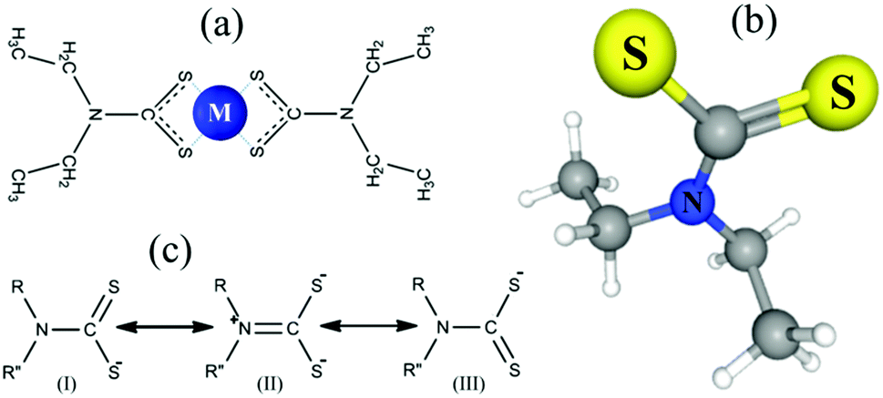 | ||
| Fig. 1 Structure of a symmetric bidentate complex with metal M (a), 3D conformer (PubChem) (b) and resonance structures (c) of N,N-diethylcarbamodithioate. | ||
The features of DTC complexes are associated, in particular, with the fact that the central metal ion M can form its coordination sphere consisting of four sulfur atoms in various ways. Ligands can bind to the central metal ion with either monodentate asymmetrical or bidentate symmetrical bonding. This is because DTC can exist in different resonant forms (Fig. 1).54 In forms (I) and (III), there is a single bond between the nitrogen atom and the carbon atom carrying two S atoms, and, accordingly, the delocalization of the charge between carbon and the two sulfur atoms. In form (II), the contribution of the lone pair on the nitrogen (N) atom leads to the formation of a double bond between N and C, connected to two S atoms carrying negative charges. In this form, nitrogen has sp2 hybridization, which determines the planar geometry of the coordination environment of the metal; the lone pair on the nitrogen p-orbitals is delocalized within the π-orbitals of the C![[double bond, length as m-dash]](https://www.rsc.org/images/entities/char_e001.gif) N double bond.
N double bond.
Homoleptic complexes formed by a bidentate symmetric bond arise when two identical DTC ligands coordinate around a divalent ion.55 IR spectroscopy is usually used to identify the monodentate or bidentate nature of the binding.56 It was shown that in the case of the copper and zinc complexes, bidentate symmetric binding of ligands takes place: stretching vibrations of the DTCs of transition metal complexes (including Zn and Cu) indicate a significant double bond in S2CNR2 and the chelating nature of CS groups.57 Such symmetric complexes are more stable than with monodentate ligands due to the chelate effect.58 The chelating effect has both enthalpy and entropy components. The entropy contribution is due to the distortion of the bond angles in the ligand molecule during the formation of a coordination sphere of certain symmetry, the possibility of rotation with respect to certain bonds, etc. The enthalpy component for ligands containing a dithiocarboxyl group with trivalent nitrogen is partially associated with the formation of π bonds with the metal cation; due to the combined effect of the σ and π interactions, the effective charge on the cation decreases. Thus, in form (II) with a bidentate symmetric bond, the properties of the DTC complexes depend on the electronic configuration of the central ion.59 These features lead to the difference in behavior of the complexes of copper and zinc in the gas-phase reactions near the substrate discussed below.
According to,60 the kinetics of the DTC–Cu–DTC decomposition process is well described by a first-order reaction – it is a monomolecular process representing an intramolecular rearrangement leading to the formation of a metal sulfide.57,61 The process begins already at a temperature of more than 140 °C directly in the gas phase. For copper complexes, the most negative values of the change in entropy are observed,57 which agrees well with the change in the orientation of the ligands around the metal ion during intramolecular rearrangement during decomposition.62,63 In the case of Zn, the reaction order is two, which implies a bimolecular process, including a rearrangement within the coordination sphere due to the collision of two complexes in the gas phase or a collision with a substrate. This, in particular, means that in the case of Zn complexes, the reorientation of the ligands does not lead to a decomposition of the complex, and pyrolysis in the gas phase is unlikely. The higher stability of the zinc complexes with dithiocarbamates may be due to its outer electron shell d10, which forms a coordination polyhedron with a high potential barrier to rotation around the S2CNR2 bond. Since overcoming this barrier is necessary for breaking part of the M–S coordination bonds through the rotation of the ligands (as in the case of copper), Zn stabilizes a more energetically favorable conformation, the destruction of which is possible only due to a collision. This property of zinc dithiocarbamate complexes seems to be of fundamental importance for the practical implementation of the CVD method. Indeed, unlike copper complexes that can efficiently decompose in the bulk of the gas phase, the predominant pyrolysis of Zn dithiocarbamates will occur on the surface of the substrate, since bimolecular collisions in the gas phase can be disregarded under the condition of low concentration of DTC complexes in the gas phase.
The dependences shown in Fig. 2 are constructed from the previously experimentally obtained family of isotherms (dependences of the film growth rate on the precursor flux intensity at a constant substrate temperature) for various substrate temperatures in the range 200–340 °C.48 The low-temperature region I is a kinetic regime (so called surface reaction limited, rate limited, kinetic limited) – the film growth rate is limited by the rate of chemical reactions on the surface. The average region of temperatures II is determined by the diffusion regime, i.e. the film growth process is limited by the transfer of the mass of the active precursor to the region of the reaction front (so called diffusion limited, mass transfer controlled, gas-phase transport or feed-rate limited). In the temperature regions I and II, the process of heterogeneous pyrolysis of DTC complexes on the surface of the substrate with the formation of a film dominates. In these areas, the highest quality of polycrystalline films is ensured: mirror surface, high adhesion to substrates; in region II, in addition, a higher growth rate is usually observed.
 | ||
| Fig. 2 Dependence of the film growth rate (on a logarithmic scale) on the inverse temperature of the substrate at various precursor flux intensities for ZnO–ZnS films (1–0, 10; 2–0, 15 mg cm−2 s−1). | ||
The film growth rate VI in the kinetic regime depends on the precursor concentration in the reaction space C, however, the growth is limited by the process with activation energy Ea and follows an exponential dependence on the inverse temperature 1/T (Fig. 2). With increasing temperature, when VI reaches its maximum value, the limiting stage of growth is associated with the process of delivery of the active precursor to the reaction front, and the delivery rate of which VII is proportional to the square root of the temperature (Fig. 2). The coefficient of proportionality, as in the kinetic mode, depends on C and the diffusion coefficient in the gas phase, the temperature dependence of which is rather weak in the temperature range commonly used in MO-CVD. The lower the temperature, the greater the effect of the decomposition process on the surface of the substrate; the higher the temperature, the more the film growth rate is limited by the mass transfer and decomposition of the precursor in the gas phase. A more detailed statistical and probabilistic consideration of this process can be found in.64–67
In the kinetic regime I, the key is to maintain temperature uniformity both, in the reaction volume and on the surface. Under this condition, it is possible to obtain large area thin uniform films, including on flexible substrates, such as electrically conductive polymer plates transparent in the visible region. That is why the application modes at the lowest possible temperature are of particular interest, especially if it is possible to find ways to increase the growth rate while maintaining the structural perfection of the coating.
It should be noted that, as follows from Fig. 2, an increase in the precursor flux leads only to an increase in the film growth rate, while the general form of the dependence remains unchanged. According to the structural analysis data,47,68 both amorphous and textured films are deposited in regions I and II; in some cases, even epitaxial growth is observed on single-crystal substrates. In the transition from the kinetic region I to the diffusion region II, the growth rate reaches the highest values. However, with increasing temperature, the probability of defects generation also increases, since the process depends on the shape of the flow. The decrease in growth rate in region III (the so-called evaporation limited, equilibrium limited) is usually associated with the precursor depletion mode. This process may be, in particular, due to the fact that the temperature of the gas becomes high enough, far enough above the surface that gas-phase pyrolysis of the hydrides becomes important and solid particulate can form without depositing on the substrate. This parasitic spontaneous nucleation, along with increased desorption of the reactant species, takes place at the expense of the desired deposition and leads to a reduced growth rate, as shown in Fig. 2. Thus, in region III—the region of high temperatures—two processes of the formation of the final product are observed simultaneously: heterogeneous on the substrate and homogeneous in volume. As a result of this, the quality of the films is noticeably deteriorated due to the hit of the particles formed in volume on the substrate: the growth rate of the film slows down, the adhesion of the film to the substrate decreases; the roughness of the film increases and the ordering of crystallites decrease.
3. Experimental section
3.1 Chemicals and reagents
Zinc and copper N,N-diethyldithiocarbamates were synthesized in accordance with procedure69 from an aqueous solution of sodium N,N-diethyldithiocarbamate 3-aqueous (analytical grade) and aqueous solutions of zinc chloride (analytical grade) or copper chloride (Chemically pure, cp), respectively. Pyridine (cp) (CAS No. 110-86-1) was used as a solvent for the obtained DTC complexes.3.2 Thin films fabrication
Zinc oxide films were prepared using a modified CVD process, when a solution of an organometallic precursor is supplied in the liquid phase to a reactor at atmospheric pressure (MetallOrganic – Atmospheric Pressure – Direct Liquid Injection-Chemical Vapor Deposition, MO-AP-DLI-CVD). The main factor limiting the growth rate of films at atmospheric pressure is the mass transfer of the precursor and the volatility of the decomposition products. Due to the numerous collisions of the gas molecules at atmospheric pressure, the average mean free path is only about 40 nm. Therefore, the precursor in the liquid phase carrier is force sprayed into the chamber through the injector (Fig. S1, ESI†). The injector is made of glass; the diameter of its nozzle is 100–150 nm; the pressure of the carrier gas (usually air) is regulated in the range of 0.6–1.2 atm.In the case of an excessive increase in temperature in AP-CVD, and, accordingly, pressure, film growth is greatly slowed due to the fact that molecules in the gas phase interfere with the desorption of the gaseous decomposition products and the difficulty of adsorption of new molecules. In this case, due to the sufficiently high thermal conductivity of the gas phase in AP-CVD, it is necessary to take into account not only the surface temperature of the substrate, but also the temperature of the gas mixture, since pyrolysis can occur at high concentrations of precursor vapor (see Fig. 2, region III). Thus, an increase in the temperature and/or vapor concentration of the starting compound can lead to an increase in the deposition rate, but also a slowdown in the film growth rate owing to the intensive growth of particles in the gaseous phase.
Considering these factors, we selected synthesis temperatures corresponding to the conditions under which the film growth is controlled by the surface process (220 °C, low temperature, LT, region I in Fig. 2) and the mass transfer of the precursor in the near-surface region (255 °C, high temperature, HT, region II in Fig. 2). HT films were obtained at a doubled flow rate of reagents as an increase in the substrate temperature is usually used to increase film growth rate (see Fig. 2), and also in order to find out whether this leads to an increase in the coating rate while maintaining its structural perfection.
Thin (0.35–0.65 μm) ZnO–ZnS films, including those with the addition of Cu, were obtained by spraying a 0.1 M solution of Zn(DTC)2 in pyridine onto heated (up to 220–260 °C) glass substrates C-48 and Si(111) with native oxide in a quasi-closed volume70,71 in an air atmosphere. A quasi-closed volume is created by a quartz cylinder with a diameter of 102 mm and a height of 80 mm, which limits the reaction zone, providing a certain vapor pressure of the incoming precursor and free removal of reaction products (Fig. S1, ESI†). The technological parameters of the obtained films are shown in Table 1.
| Sample label/substrate temperature/Cu-content (% w/w) | Feed rate (ml min−1) | Film thickness (nm) | Growth rate (nm min−1)/efficiency (nm ml−1) | Film phase composition | |
|---|---|---|---|---|---|
| Substrate Si/SiO2 | Substrate/glass | ||||
| LT | |||||
| 220 ± 5 °C | 1.0 ± 0.1 | 500 ± 27 | 29/29 | 14% ZnS | 68% ZnS |
| Cu-DTC:0.0 | 86% ZnO | 32% ZnO | |||
| LT:Cu | |||||
| 220 ± 5 °C | 1.2 ± 0.1 | 650 ± 27 | 46/38 | ZnO-100% | 2% ZnS |
| Cu-DTC:0.2 | 98% ZnO | ||||
| HT | |||||
| 255 ± 5 °C | 2.0 ± 0.1 | 350 ± 27 | 50/25 | 77% ZnS | 64% ZnS |
| Cu-DTC:0.0 | 23% ZnO | 36% ZnO | |||
| HT:Cu | |||||
| 255 ± 5 °C | 2.0 ± 0.1 | 350 ± 27 | 35/18 | ZnO-100% | 19% ZnS |
| Cu-DTC:0.2 | 81% ZnO | ||||
The film thicknesses were determined using a MII-4 interference microscope and spectral ellipsometry. The film growth rate in nm/min was calculated as the ratio of the film thickness to the time of its growth. In order to characterize how efficiently the reagents are used to form the film coating, the concept of film growth efficiency (nm ml−1) was introduced, which was defined as the ratio of the growth rate (nm min−1) to the feed rate of the starting material to the substrate (ml min−1).
3.3 Characterization methods
The diffraction peak parameters were determined by approximating a Gaussian type curve using Origin Pro 7.5 (Origin Lab Corporation).
The crystalline quality of the films has been evaluated by calculating the average crystallite size D and average micro strain ε developed in nanostructured thin films by using Debye Scherrer's approach.72–76 It should be noted that the classical version of this approach assumes that the sample is polycrystalline with a stochastic orientation of individual crystallites. Since, in the case under consideration, the films are textured in the direction perpendicular to the plane of the substrate, all the calculation results presented in this article refer only to the average micro strain ε(002) and average size D(002) along the c axis of the crystal. To estimate the degree of texturing of the films, we used the ratio of the intensities of the (002) and (101) reflections. For a nanoparticle samples with a random orientation on the surface, the intensity ratio (002)/(101) is approximately 0.3.76
To measure the TAE, a surface acoustic wave was excited in the z-direction of the yz-LiNbO3 piezoelectric substrate using an interdigital transducer at a frequency of 37 MHz, a duration of 1.5 ms, and an aperture of 1.8 mm (ESI,† Fig. S2). The gap between the semiconductor and the piezoelectric was ensured by a system of supports 200 nm high, etched by the ion beam directly on the surface of the LiNbO3 substrate.
Low-resistance Si p-type samples of 5 × 2 × 0.3 mm3 size were cut from standard Si(111) wafers with a layer of natural silicon oxide. An analysis of the features of the TAE showed that the interface is in a mode of weak depletion due to the charge of the biographical states of the surface.
4. Results and discussion
As noted above, the driving force of the decomposition process and the subsequent surface reaction is the temperature in the immediate vicinity of the surface reaction front. As can be seen from Table 1 and Fig. 3, depending on the temperature and the presence of copper ions in the reaction volume, it is possible to obtain both single-phase ZnO films and binary films with different ratios of crystalline phases of ZnS and ZnO. The most intriguing result is that the film growth efficiency remains almost unchanged with increasing temperature and feed rate, while the addition of only 0.2% w/w DTC-Cu leads to the opposite effect for temperature ranges I and II (Fig. 2) – at 220 °C, the growth rate increases (1.5 times), and at 255 °C it decreases by more than 40%. Clarifying the cause of this effect requires a detailed analysis of the morphology and surface properties of these films. | ||
| Fig. 3 X-Ray diffraction patterns of ZnO/ZnS(:Cu) films obtained by pyrolysis of dithiocarbamates at atmospheric pressure (growth parameters are shown in the figures). Insert: The relationship between the wurtzite geometric structure and crystal growth orientation. The ZnO(002) orientation is straight off the substrate with O- or Zn-polar surfaces, while the different orientations correspond with in-plane (e.g. nonpolar (100) with a rectangular unit cell) and out-of-plane components (e.g. (101) or (103)) of the hexagonal zinc oxide nanorods. | ||
4.1 Structural properties of films
According to the XRD data (Fig. 3), the obtained films are polycrystalline with one (ZnO) or two (ZnO and ZnS) phases depending on the conditions of their formation and the type of substrate; ZnO phase have a hexagonal wurtzite structure. The films have a pronounced texture: the intense reflex from the (002) ZnO plane (at 34.39°–34.41°) or (002) ZnS plane predominates on the diffractograms. The large value of the half-width of the reflections (FWHM = 0.35–0.50°, Tables S1–S4, ESI†) indicates relatively small areas of coherent scattering in the polycrystalline films. The computed results of the average crystallite size (D(002)) and average micro strain (ε(002)) developed in nanostructured thin films are given in Table 2 for ZnO and in Table S5 (ESI†) for ZnS phases.| Sample label/substrate temperature/Cu-content (% w/w) | Average crystallite size D(002) (nm)/silicon/glass | Average micro strain ε(002)·10−5/silicon/glass | Surface texturing (002)/(101)/silicon/glass |
|---|---|---|---|
| LT | |||
| 220 ± 5 °C | 23.2/17.6 | 552/726 | 39/full textured |
| Cu-DTC:0.0 | |||
| LT:Cu | |||
| 220 ± 5 °C | 24.5/22.6 | 523/566 | 51/105 |
| Cu-DTC:0.2 | |||
| HT | |||
| 255 ± 5 °C | 20.5/19.7 | 625/654 | 15/full textured |
| Cu-DTC:0.0 | |||
| HT:Cu | |||
| 255 ± 5 °C | 25.2/23.8 | 508/537 | 7/686 |
| Cu-DTC:0.2 | |||
A characteristic feature of the diffraction patterns is the presence of an average intensity reflection from the (103) ZnO plane and multiple reflections of insignificant intensity from the (100), (101), (102) planes, etc. The angular position of the peaks is consistent with JCPDS data for nominally pure zinc oxide (JCPDS, No. 36-1451).
The well textured structure of the films on both amorphous glass and silicon (with natural silicon oxide) indicates that the substrate only partially exerts an orienting effect on the structure. In this case, the growth of the hexagonal ZnO nanorod that is perpendicular to the substrate occurs under conditions when the growth process is controlled by the process of crystal lattice formation.
Indeed, the formation of the oriented regions of the crystal along the c direction is in good agreement with the minimum energy of the outer sides of the hexagonal columns, which is the energetically most favorable surface of ZnO with its non-polar rectangular surface unit cell.82–84 Consequently, this termination forms the dominating portion of the surfaces in nanoscale structures; it exhibits no electrostatic instabilities and their relative position is limited only by spatial blocking.
In contrast to the side faces, the upper polar terminations exhibit a hexagonal surface structure (O- or Zn-polar). Assuming that the ions are in their bulk oxidation state, each ZnO double layer carries a dipole moment. As a consequence, the bulk truncated polar structure is not stable. To reduce the instability, there has to be a redistribution of charges, which usually happens by either a structural rearrangement or the loss/capture of passivating ions at the surface.
A number of additional reflexes are also observed (Fig. 3): a polygon (100) structure of ZnO gives a component entirely in the plane of the substrate; a pyramid-like (101) as well as (102) and (103) are combinations of the in-plane and out-of-plane components (Fig. 3). It should be noted that (102), and (103) are reflections from the planes, which can also be the result of the intersection of the hexagonal columns (twinning), the growth direction of which is at some angle with the plane of the substrate.85 Moreover, the rather high intensity of the reflection (103) is probably due to the geometry of the precursor flux in the surface region of the sample, part of which propagates along the growing surface from the center to the periphery. Indeed, some authors note that the origin of the (103) diffraction might be related to the surface structure of the film: the surface structure could be affected by the movement or diffusion of atoms at the final stage of the sputtering process and vacancies created by the out diffusion of oxygen from the network, which induces the growth along the (103) crystallographic orientation.86
Similar X-ray diffraction patterns for films with dominant (002) and (103) reflections were also noted by other authors who used similar technological methods for the preparation of zinc oxide films based on the pyrolysis of organometallic compounds in the gas phase87–96 or ZnO thin films grown by pulsed laser deposition.97,98
4.2 Effect of the substrate on the film structure
Samples obtained in one sputtering cycle, but on different substrates, demonstrate a number of characteristic features. As can be seen from Fig. 3, the diffraction patterns of the films on glass substrates are characterized by a more pronounced halo (amorphous phase), a lower intensity of the diffraction peaks and their larger half-width. Moreover, in most cases the ZnS phase is observed, and the number of diffraction peaks is less than in the case of silicon substrates with a thin layer of natural oxide. In general, we can conclude that the films on glass substrates have a slightly larger contribution from the amorphous phase and the polycrystalline part is characterized by smaller the average crystallite size. Moreover, in all cases, the position of the peak is slightly less (0.01–0.05°) for films on glass substrates relative to films on silicon especially for the HT films (255 °C) or the reflection (103). This effect may be due to a more inhomogeneous structure of the glass surface in comparison with single-crystal silicon wafers.The well textured structure of the films on both amorphous glass and silicon (with natural silicon oxide) indicates that the substrate only partially exerts an orienting effect on the structure. In this case, the growth of the hexagonal ZnO nanorod that is perpendicular to the substrate occurs under conditions when the growth process is controlled by the process of crystal lattice formation.
4.3 Effect of substrate temperature and reagent flow rate
A simultaneous increase in the substrate temperature (from 220 to 255 °C) and the feed rate of reagents (from 1 to 2 ml min−1) does not lead to qualitative changes in the structure of the films (Tables 1 and 2). Thus, although an increase in temperature stimulates the growth of the crystalline phase (Table 2) for films obtained without the addition of copper, this effect cannot compensate for the increase in the flow rate, as a result of which ZnS is formed on the surface (Table 1). In the presence of copper in the reaction volume, the diffraction patterns of the films correlate well with each other, with only a slight difference in the reflection from the ZnS phase at a higher temperature, the presence of which is due to the reasons described above. The features of the film growth at a higher temperature allow us to conclude that the process of ZnO film formation in the course of synthesis is not determined by the transformation in the volume of the already formed ZnS film, but occurs either by replacing sulfur with oxygen in the surface layer of the reaction front, or the ZnO film grows independently from ZnS through a surface reaction of reagents coming from the gas phase.4.4 The effect of low-quantity Cu addition in the reaction volume
A comparison of the influence of temperature, the feed rate of the reagents, and the type of substrate with the influence of a small (only 0.2% w/w) amount of copper in the reaction volume unambiguously indicates that it is the latter effect that has the strongest impact on the quality of the obtained films. According to XRD data, ZnO/ZnS:Cu films on Si substrates are polycrystalline, single-phase, highly textured and have a hexagonal wurtzite structure. An analysis of the results indicates that the addition of copper ions does not shift the (002) reflection, which corresponds to the preferred growth direction along the c axis of the crystal lattice, for both silicon and glass substrates. This conclusion is also valid for the second largest reflection (103). Thus, it can be argued that the addition of copper to the reaction volume does not lead to significant variations in the ZnO lattice parameters.It was also observed an increase in the coherent scattering region of X-ray radiation (the average crystallite size (D(002))) on all substrates has been observed when copper ions are present in reaction volume (Table 2). This allows us to conclude that the presence of copper ions stimulates the growth of larger crystallites in polycrystalline ZnO films simultaneously with decreasing the average micro strain (ε(002)) developed in nanosized crystallites.
This data is not consistent with the assumption that copper ions, due to their smaller cationic radius (Cu2+ 80 pM), effectively replace Zn2+ ions (83 pM) in the ZnO crystal lattice. Such aboard “substituted” structures are either less thermodynamically favorable than the natural lattice of the material, or the structure of such regions should be distorted. This allows us to suggest that copper ions do not replace zinc ions in the regions of ordered ZnO lattice, but accumulate in the polar surfaces, decreasing the excess of surface energy by passivation the dangling bonds of the (002) ZnO face.
4.5 Charge state features of ZnO/ZnS(:Cu) coatings
Table 1 and Fig. 4 show the results of the investigation of the TAE in Si-ZnO/ZnS structures in an air atmosphere under illumination (TAE value at zero illumination power corresponding to measurements in the dark). The results show that all the samples are characterized by a negative sign of the TAE value. This means that the high-resistivity surface region in silicon formed at the Si-ZnS/ZnO interface has a p-type conductivity. | ||
| Fig. 4 Dependences of the acoustoelectric electromotive force value specific for transverse acoustoelectric effect (TAE) on the illumination power (wavelength λ = 525 nm) for LT and HT ZnO/ZnS samples with and without copper. Inset: Schematic models of the ZnO/ZnS film and measurement configuration (SAW-surface acoustic waves, LED-light emitting diode; the gap between the semiconductor (Si) covered by ZnO/ZnS film and the piezoelectric (lithium niobate) was ensured by a system of supports 200 nm high, etched by the ion beam directly on the surface). | ||
It follows from Table 1 and Fig. 4, that the value of TAE most strongly depends on the presence of Cu2+ ions during synthesis and, to a lesser degree, on the substrate temperature. The highest values of TAE were obtained at LT/HT (220/255 °C) with the addition of copper; an increase in the value of TAE in the dark was up to 5 times higher in this case compared to copper free synthetic conditions. The variation of the TAE response of the samples obtained at different temperatures did not exceed 25–30%, which may be due to a number of factors. For example, the difference in the thickness of ZnO/ZnS films leads to a difference in the amplitude of induction induced by SAW's evanescent wave on the surface of the semiconductor and affect the total surface area of the film, morphological features, etc. We have discussed some of these issues earlier in.77
It is well known that the magnitude of the acoustoelectric-emf mainly depends on the concentration and mobility of the free carriers, charge on the surface states, and the initial bending of the carrier and valence bands.77 The relationship between the magnitude of the bending of the semiconductor bands and the TAE value was determined experimentally99,100 and substantiated theoretically.101 In the present case, the analysis of the sign, value, relaxation time and TAE signal waveform leads to the following conclusions: (i) the TAE is generated by positive sign carriers in silicon, (holes, p-type); (ii) the analysis of the ratio of the trap and concentration components of the TAE showed that the interface is in a mode of poor depletion due to the charge of the biographical states of the surface and (iii) the value of the TAE is directly related to the charge in the ZnS/ZnO film (the trapped component of the TAE plays an essential role in the observed processes – large TAE values are characterized by longer relaxation times).
Thus, it can be assumed that the observed values of the TAE are related to the presence of a positive charge distributed in the ZnO/ZnS film. The change in this charge leads, through the field effect, to a change in the initial bending of the bonds and, accordingly, the resistivity of the near-surface region of the space charge of the semiconductor and, finally, to the magnitude of the acoustoelectric-emf. As a result, small changes in the value of the charge localized in the outer surface are transformed into near-surface conductivity of the semiconductor, which is easily measured by the non-contact method.
In order to determine the position of this charge in ZnO/ZnS films, we have utilized layer-by-layer etching of the ZnO/ZnS films in a weak water solution of hydrochloric acid (0.2% v/v). Similarly to other samples investigated in,77 the greatest influence on the value of the TAE is caused by etching in the initial section (Fig. 5), – a sharp drop in the value of the TAE is observed when the thickness of the film decreases by approximately 15–20% (ca. 150 nm, it fits well with the height of the surface profile according to the AFM data61). This supports the point that the primary cause of the high value of the TAE in ZnO/ZnS(:Cu) films is the surface charge localized on the outer surface of the ZnO films.
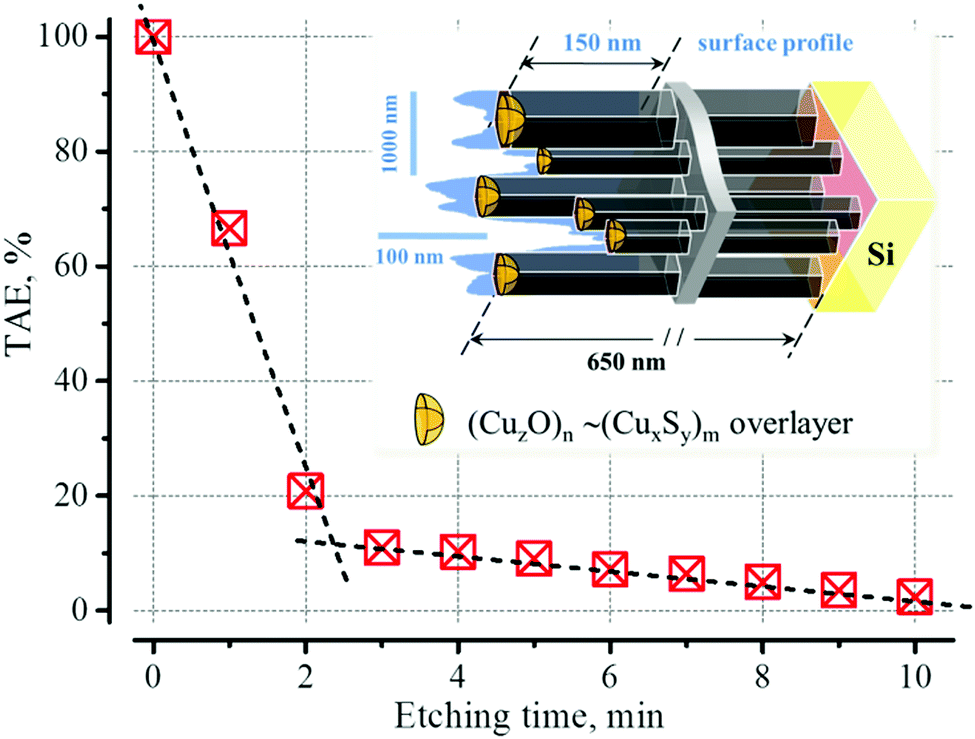 | ||
| Fig. 5 Dependence of the TAE value on the etching time of the LT:Cu sample in a weak hydrochloric acid solution (0.2%) until the film is completely etched (ca. 11 min). Inset: Superposition of the surface profile (maximum profile height ca. 150 nm according to the AFM imaging) and schematic model of the film. | ||
The TAE measurements results show, that the effective charge in the near-surface region of ZnO/ZnS films is positive. The origin of this charge has been attributed to either adsorbates and defects of the biographical origin, or it was considered an “intrinsic” property of the respective surface (which can be either Zn-rich, O-rich or anything in between). The etching experiments show that after etching, the charge slowly increases over time when the sample is exposed to an air atmosphere. This fact indicates that the surface charge, at least partially, has an adsorption nature. The main candidates capable of forming charged centers on the ZnO/ZnS surface include oxygen, water, and hydrogen at least. Since the purpose of this work was not to establish the nature of this charge, we therefore only briefly introduce the possible mechanisms of the charge formation. The reason for this seems to be the richness of defect physics in these materials with a plurality of possible intrinsic and extrinsic defects.
The surface states are typically associated with the oxygen centers of the adsorption origin, the negative charge of which is due to the capture of electrons from the near-surface region of the material.102,103 However, oxygen centers mainly determine the charge and conductivity of the surface region of oxide semiconductors at sufficiently high temperatures (300 °C or more). At the same time, for example, ZnO nanoparticles have positive charge in aqueous media because protons from the environment are likely transferred to the particle surface, leading to a positive charge from the surface ZnOH2+ groups (ZnO typically has neutral hydroxyl groups attached to its surface, which plays a key role in its surface charge behavior).104–107 Moreover, it was shown that ZnO samples synthesized by the hydrothermal method were all positively-charged on the surface.108 Data using Kelvin probe force microscopy also confirm the presence of positively charged regions on the surface of zinc oxide films.109,110 All this indicates that, under normal conditions, centers of various nature can be formed on the ZnO surface, the effective total charge of which is determined by the preparation conditions, storage, additional processing, etc.
An equally important mechanism of surface charge formation in ZnO is the features of the electronic structure as an “intrinsic” property of the respective surface. For example, in111 it is argued that the bulk truncated polar structure of ZnO is not stable and can only exist with hydrogen adsorbed on the surface. Therefore, it is probable that the measured surface has been stabilized by hydrogenation. Indeed, in recent years, hydrogen has been recognized as the most probable interstitially, trapped, or adsorbed at the surface dominant donor in zinc oxide, which suggests that atomic hydrogen predominantly binds to surface oxygen atoms to form O–H species.112–114 Consequently, a charge accumulation layer at the ZnO surface is created. Similar layer formation at ZnO surfaces was also found after irradiation with ultraviolet (UV) light,115 as well as the adsorption of water and methanol.116 Thus, it appears likely that there are several ways to introduce surface donors on ZnO as they play a role in surface stabilization and their formation is energetically favorable.
Taking into account the fact that the magnitude of the acoustic emf significantly increases in the presence of copper ions during synthesis, the assumption that the presence of copper cations or copper-containing compounds on the outer surface of ZnO/ZnS films is also an important factor in the formation of a region of positive charge on the surface is logical.
4.6 Features of the TAE under illumination
The features of the TAE value based on irradiation intensity are presented in Fig. 4 and Fig. S3 (for 470 and 635 nm, ESI†). In the context of this work, it is necessary only to note that the formation of a large surface charge on the outer surface of the film leads to the stabilization of the barrier height at the interface between the ZnO/ZnS film and silicon (by means of the field effect).77 As a result of this, the generation of nonequilibrium charge carriers under external irradiation is not able to compensate for the depletion caused by the separation of carriers by the surface barrier. This property is extremely interesting and can find wide practical application for the development of solar cells based on light concentrators, since they will increase the generation of charge carriers without substantially changing the height of the barrier. It is worth highlighting that an “insignificant” addition of copper ions in the synthesis process dramatically changes the photophysical processes at the interface.4.7 Adsorption properties of ZnO/ZnS(:Cu) films
As noted above, water vapor affects surface states in ZnO films.116 However, in our study, we did not find any “Cu-specific” effects of water. At the same time, we found that under the saturated vapor of water, the largest change in the TAE was observed for samples with small values of acoustoelectric-emf in the dark, while the samples with large dark responses practically did not respond to water vapor (data not shown). This aligns well with the discussion above, that the centers with surface-bound hydroxyl groups and/or hydrogen may be at least partly responsible for the formation of a positive surface charge on the ZnO/ZnS surface. Moreover, the fewer the number of such groups on the surface, the greater the observed effect of exposure in water vapor.The exposure of the films under consideration in a stream of headspace containing about 10% ammonia in water shows that the donor abilities of the amine are dominant in the response. As can be seen from Fig. 6, during the inlet of ammonia vapors, the TAE signal rapidly drops, which confirms the surface nature of the charge. The character of the dependence is qualitatively similar for all samples. This behavior is due to the fact that the donor abilities of the lone-electron pair of ammonia can neutralize the positively charged surface centers, and thus reduce the value of the TAE. As can be seen from Fig. 6, copper-containing samples are characterized by several times greater reactions to ammonia, but the relative values of their changes are much less (within 30%). This indicates that the actions of ammonia and water are proportional to the total number of charged surface centers, the interaction with which is reversible (physical adsorption). Thus, the availability of Cu centers on the surface cannot be identified by those chemical compounds.
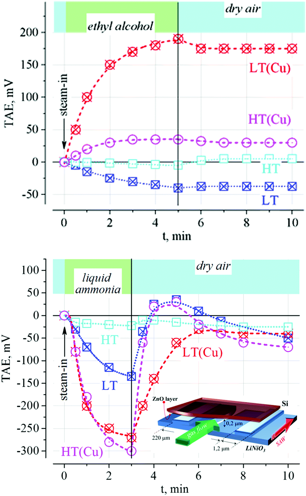 | ||
| Fig. 6 Dependence of the absolute value of the change in the TAE signal for LT and HT ZnO samples with and without copper with saturated vapors of ethyl alcohol (top) and liquid (10% ammonia in water) ammonia (bottom). Inset: Schematic models of the measurement configuration. | ||
In,117–120 it was shown that the process of interaction of ethyl alcohol with the surface of ZnO consists of two stages: (1) adsorption of gas molecules on hydroxyl groups of the acid type and, (2) their subsequent oxidation with the participation of negatively charged oxygen, as a result of which free electrons are formed, and the conductivity increases. The behavior of the samples obtained in the absence of copper ions aligns with this mechanism: exposure to alcohol vapor leads to a decrease in the TAE signal of the samples obtained both at low and high temperatures owing to a decreasing positive surface charge by the trapping of the generated free electrons. The change in the value of the TAE indicates that the efficiency of the process is low at 20 °C.
For the samples obtained in the presence of copper ions, the behavior of the TAE response is fundamentally different from that described above. The exposure to alcohol vapor leads to an irreversible increase in the signal. The reason for this behavior may be due to the presence of copper compounds on the film surface. Indeed, the interaction of copper oxide with alcohol vapors can lead to dehydrogenation of ethanol with the release of copper as positively charged ions.
5. The mechanism of acceleration of crystal growth, refinement from precursor's residual and improvement of the ZnO crystalline quality by the small addition of copper
Comparison of the results of the study of morphological and functional features of ZnO/ZnS films obtained by pyrolysis of diethyldithiocarbamates in the gas phase allows us to draw the following conclusions:(I) When 0.2% w/w copper is added to the reaction mixture during the synthesis of ZnO LT films, (i) the growth rate and reagent efficiency, (ii) the structural perfection and “purity” of the ZnO films are increased. In this case, the TAE value (correlating with the positive charge on the external surface) increases several times.
(II) When the temperature rises to the value corresponding to the diffusion regime, the addition of 0.2% copper leads instead to a decrease in the growth rate and efficiency of the use of reagents. Moreover, with an equivalent initial amount of starting reagents in LT and HT modes, HT films are almost twice as thin as LT (Table 1). Moreover, the absolute values of the growth rates in HT and LT modes are comparable in magnitude, despite a twofold increase in the reagent flux for HT samples. This leads to an increase in the contribution of the ZnS phase in the sample without copper, but does not change the composition for samples with copper, where only the ZnO phase is observed in the HT mode. The charge on the outer surface is somewhat smaller compared to the samples obtained in the kinetic region, however, this may be due to different “branching” of the film surface at different thicknesses. The charge ratio in the presence and absence of copper is similar to the LT mode.
(III) The analysis of the functional properties of the surface indicates that when copper is added to the reaction volume, the samples exhibit characteristics of the presence of copper compounds on their surface.
Summarizing the observation data, we can conclude that Cu-containing surface clusters as a catalyst stimulate the growth of the ZnO crystalline phase. In this case, it is likely that copper do not penetrate into the crystal lattice of the material, but induces the pyrolysis of DTC-Zn complexes (limiting process) in the kinetic mode, which leads to faster decomposition of the complex and an increase in the concentration of the reactive components (ZnS). If diffusion mass transfer at a higher temperature is limiting, then copper compounds “clean” the surface by displacing the surface captured sulfur again into the gas phase and, thus, slowing down the overall ZnO growth process.
The general trends noted by the authors of many publications correlate well with the results of this research. Briefly, these features are:
(1) Findings regarding copper distribution and diffusion beyond the surface layers are often conflicting. On the one hand metals like Cu, Ag or Au, are fast-diffusing impurities in all semiconductors including II–VI compounds, like ZnS or ZnO. The diffusion of Cu into the ZnS lattice is supposed to be governed by interstitial and substitutional mechanisms.123–125 It was confirmed that the ion exchange mechanism of Zn2+ by Cu2+ occurs on the surface, followed by a redox reaction of the adsorbed Cu2+ into Cu+ and S2− into S−, which leads to the formation of a Cu(I)–sulfide layer on the sphalerite surface.126 Moreover, it was found that the copper uptake was lower in the presence of oxygen.127–130 Finally, it is possible to conclude that CuS/Cu2S might exist on the surface but their migration deeper is a low probability effect in air.
In the case when copper content is high, in particular, exceeds ca. 6–7 at%, it is energetically favorable for excess atoms to combine into copper clusters (interstitial segregation) or Cu/Zn clusters and increase the number of defects.131–134 In the case of the formation of a solid solution of copper and zinc oxides, significant lattice deformations of zinc oxide are observed when copper is placed in the zinc matrix.135
(2) The active phase of most copper–zinc materials is the centers of copper, in one form or another, located on the surface of zinc oxide/sulfide(s).136,137 Moreover, on the surface of the ZnS or ZnO films decorated with copper, a great variety of individual centers (Zn/Cu–H and Zn/Cu–OH) and their complex structures (Cu+–O–Zn) were observed.138–140
(3) Most of these materials exhibit high or even maximum (Cu-containing catalysts) activity in the range of 220–280 °C. This is typically associated with the participation and interconversion of Cu+, Cu2+ ions and metallic copper; this changes not only the electronic structure, but also the morphology of the material. It is in this temperature range that CuO (150–230 °C), Cu2O (220–250 °C) and metallic copper (more than 250 °C) coexist in copper–zinc–alumina catalysts.141 It is important that without ZnO there is no change in the valence of copper under similar conditions.
(4) It was shown that by Cu-doping, the ZnO growth mechanism was changed and the morphology tends to nano-rods array.142,143
A proposed schematic diagram of core mechanisms specific for Cu-induced interfacial processes of ZnO growth is shown in Fig. 7. Copper compounds preferably in the form of cuprous (Cu+, b.p. 1800 °C) or cupric (Cu2+, b.p. 2000 °C) oxides are located on the surface and (CuxSy)s with 0.5 < Cu/S < 2 in close proximity to it. This, in particular, is due to the fact that the pyrolysis reactions of copper dithiocarbamates can take place as well in the gas phase depending on the temperature of the surrounding reaction space. These compounds act as an activator of the pyrolysis of zinc complexes and stimulate the conversion of ZnS to ZnO, according to substitution reactions typical of these compounds. It should be noted that a similar “catalytic” effect of transition metals on the thermal decomposition of the precursor, which leads to an increase in the film growth rate, was observed earlier for other systems.121
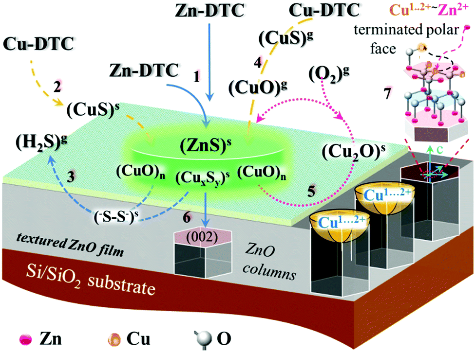 | ||
| Fig. 7 Schematic diagram of core processes illustrating the function of copper compounds during ZnO film growth: (1) bimolecular or collision induced reaction of Zn-DTC pyrolysis on the surface yielding (ZnS)s compounds on the surface (“s”); (2) monomolecular reaction of Cu-DTC pyrolysis on the surface yielding (CuS)s/(CuO)s compounds assembling in clusters on the surface (CuO)n; (3) generation of the volatile products in the reaction of ZnS or CuS with interfacial clusters of (CuO)n; (4) monomolecular pyrolysis of Cu-DTC followed by (CuS)g oxidation to (CuO)g in gaseous phase (“g”); (5) recovery of surface captured (Cu2O)s compounds by oxidation; (6) generation of ZnO crystal lattice from (ZnS)s compounds captured by (CuO)n clusters through substitution reactions in interfacial complexes (CuxSy)s with 0.5 < Cu/S < 2; (7) schematic of the atomic arrangement of the ZnO films growth resulting in Cu decorated terminated polar face: zinc ions displace coordination labile copper ions to the outer surface, forming the ZnO crystal lattice. | ||
Surface cleaning from poisonous sulfur may proceed as follows for the so-called Z-scheme assisted ZnO/Cu2O–CuO catalytic reactions.122 In line with this mechanism S2− ions from Zn2+S2− complexes can react with interfacial clusters of CuO to transform it into S22− (disulfides), and thus form volatile hydrogen chalcogenide (H2S2, b.p. 70.7 °C), which decomposes readily to gaseous hydrogen sulfide (H2S, b.p. −60 °C) and elemental sulfur.
At the end of this section, we briefly focus on the mechanism that makes it possible to explain the observed results. It should be emphasized that the process considered below dominates only at low concentrations of copper in the reaction mixture. It is known that, as the concentration of copper increases, it begins to integrate into the ZnO lattice and the structural perfection of the crystals decreases.
In chemistry of coordination compounds, the issue of the so-called principle of maximum correspondence of the ligand cavity to the ion of the complexing metal has been considered in sufficient detail.58 The commonly considered size fit is only one of several conditions that need to be taken into account in the analysis (i.e. electrostatic effects, the nature of bonds with ligands, the shape and composition of the coordination polyhedron, conformational flexibility, etc.). The second most important condition is the features of the electronic structure of the metal ion and ligands.
It is well known that transition metals tend to form covalent bonds with the significant electron density transfer to the metal. The features of this interaction are fully determined by the properties of d-electrons. Zinc ions do not have vacant d-orbitals due to the completely filled 3d10 configuration. This is a stable electronic configuration which determines both the shape of the coordination polyhedron and the almost exclusive oxidation state of zinc ions 2+. The situation with copper ions is completely different. Since the electronic configuration 3d9 is partially unfilled, copper(II) ions are a classical system in which Jahn–Teller effect is observed.58 This in particular, leads to the fact that copper(II) ions, unlike ions of other transition metals, are less “demanding” in respect of the regularity of their environment (e.g. shape and structure of the coordination sphere) and are characterized by a wide variety of structures of the ligands surrounding them.
According to the theory of the crystal field, the splitting of the d-orbitals depends on the crystalline field symmetry. In the fields of the high symmetry, the degeneracy of electronic levels takes place, which is disappears when the symmetry is lowered through the addition/elimination/change of the position of the corresponding ligands. In this case, not only the splitting itself, but also the resulting mutual energy position of the d-electron levels also depends on the symmetry of the ligand field surrounding the ion. In other words, in the presence of the vacant d-orbitals, the spatial distribution of the electron density inside the coordination sphere can change with the change in the environment, redistributing charge between different bonds.
In a crystal field of the high symmetry, due to the degeneracy and the presence of a vacant d-orbital, some spontaneous structural reconfigurations of the copper(II) complex with its immediate environment may occur. This means that in a highly ordered periodic lattice (for example, ZnO), the copper(II) ion acts as the source of dynamic instability (“jittering”), leading to local lattice deformations due to the random “hops” between the states with similar energy. At the same time, on the surface, where the lattice atoms have been broken off with a decrease in the overall symmetry of the system, the degeneracy of the electronic levels is removed and Cu2+ acts as an “adaptive” surface passivator. At the “moderate” temperatures of 200–300 °C, when on the surface of the growing crystal there is no prohibition of deformation of the forming structure that preserves its integrity, the electronic degeneracy can be as well removed by oscillations of the shape of the copper complex with its environment.
If we also consider the tendency of copper ions in an oxygen environment to have cooperative effects (including the cooperative Jahn–Teller effect, in which local distortions propagate throughout the entire structure) and the ability of copper to change the oxidation state from +1 to +4, the uniqueness of this ion as a catalyst of surface transformations is not in doubt. This suggests that the quasi-two-dimensional network of copper complexes is formed on the surface of growing zinc oxide in an oxygen environment, the nuclear configuration of which is labile and can be transformed through oscillatory movements. This kind of structure not only makes it possible to “clean” the surface from sulfur impurities, as described above (see Fig. 7), but also stimulates the formation of the thermodynamically and kinetically stable ordered structure of ZnO by replacing “jittering” copper ions in it with zinc ions complementary to the lattice and simultaneous extrusion of Cu2+ to the outer polar (002) surface (Fig. 7).
6. Conclusions
Numerous studies on “Cu-decorated” ZnO structures have been conducted over several decades, which range from the investigation of basic mineralogy (industrial flotation processes) to elucidating complex surface structures (nanostructured catalysts of methanol). However, the identity of the resulting copper-containing surface phase is still the subject of debate. The features of the growth of ZnO:Cu films found in this work are in good agreement with the “unusual” properties of such systems, caused by the formation of multivalent copper oxide clusters on the surface of crystalline ZnO. In this case, the catalytic system is maintained in an active state by controlling the ratio of copper atoms with different oxidation states, in which there are interfacial transformations “improving” the structure of the growing material, and a corresponding increase in the concentration of active, in particular charged surface centers.The above-mentioned features allow us to conclude that the addition of copper during the synthesis of ZnO films transforms the MOC-AP-DLI-CVD (Metallorganic – Atmospheric Pressure – Direct Liquid Injection-Chemical Vapor Deposition) into a catalytic enhanced MOC-AP-DLI-CVD method,36,144,145 which has been rapidly developing in recent years for producing functional materials. This procedure is similar in its configuration to catalytic methods, where the crystalline phase (in particular, nanorods or wires) is formed underneath the catalyst (“tip-growth model”),146–148 in particular copper.149 Here we reveal that the Cu clusters on polar ZnO faces affect as well the quality of semiconductor structure in the technologically interesting temperature range up to 550 K. This leads to enhanced crystallinity and monophasity of the final product, decreasing the number of subsurface defects during the growth.150 Finally, the combination of temperature optimization and chemical activation of the growth process using a Cu-based catalyst allows one to achieve high growth rates and obtain ZnO films with a high degree of texture at low temperatures even at an atmospheric pressure.
Author contributions
B. A. Snopok: conceptualization, formal analysis, writing – original draft, visualization; L. V. Zavyalova: methodology, investigation; N. P. Tatyanenko: methodology, investigation; A. I. Gudymenko: investigation, data curation; G. S. Svechnikov: writing – review & editing; V. P. Kladko: methodology, resources; A. E. Belyaev: supervision, funding acquisition.Conflicts of interest
The authors declare that they have no known competing financial interests or personal relationships that could have appeared to influence the work reported in this paper.Acknowledgements
The authors express their sincere gratitude to N. Roshina and B. Atdaev for support in film fabrication, V. L. Gromashevskii for fruitful discussion of acoustoelectric results and T. Snopok for assistance in the preparation of the present manuscript.References
- Z. C. Feng, Handbook of zinc oxide and related materials Volume One, Materials, CRC Press, 2012 Search PubMed.
- A. Janotti and C. G. Van de Walle, Fundamentals of zinc oxide as a semiconductor, Rep. Prog. Phys., 2009, 72, 126501 CrossRef.
- A. Tereshchenko, V. Fedorenko, V. Smyntyna, I. Konup, A. Konup, M. Eriksson, R. Yakimova, A. Ramanavicius, S. Balme and M. Bechelany, ZnO films formed by atomic layer deposition as an optical biosensor platform for the detection of Grapevine virus A-type proteins, Biosens. Bioelectron., 2016, 92, 763–769 CrossRef PubMed.
- A. Tereshchenko, M. Bechelany, R. Viter, V. Khranovskyy, V. Smyntyna, N. Starodub and R. Yakimova, Optical biosensors based on ZnO nanostructures: Advantages and perspectives. A review, Sens. Actuators, B, 2016, 229, 664–677 CrossRef CAS.
- H. Kim, M.-H. Oh and B. L. Yang, Photocorrosion of polyaniline–ZnS–ZnO photoelectrode for water splitting, Thin Solid Films, 2020, 693, 137678 CrossRef CAS.
- H. Wu, Z. Zheng, C. Y. Toe, X. Wen, J. N. Hart, R. Amal and Y. H. Ng, A pulse electrodeposited amorphous tunnel layer stabilises Cu2O for efficient photoelectrochemical water splitting under visible-light irradiation, J. Mater. Chem. A, 2020, 8, 5638–5646 RSC.
- K. R. Aneesiya and C. Louis, Localized surface plasmon resonance of Cu-doped ZnO nanostructures and the material's integration in dye sensitized solar cells (DSSCs) enabling high open-circuit potentials, J. Alloys Compd., 2020, 829, 154497 CrossRef CAS.
- H. Yoo, S. Kahng and J. H. Kim, Z-scheme assisted ZnO/Cu2O-CuO photocatalysts to increase photoactive electrons in hydrogen evolution by water splitting, Sol. Energy Mater. Sol. Cells, 2019, 204, 110211 CrossRef.
- K. Qi, X. Xing, A. Zada, M. Li, Q. Wang, S.-Y. Liu, H. Lin and G. Wang, Transition metal doped ZnO nanoparticles with enhanced photocatalytic and antibacterial performances: experimental and DFT studies, Ceram. Int., 2019, 46, 1494–1502 CrossRef.
- S. Goktas and A. Goktas, A comparative study on recent progress in efficient ZnO based nanocomposite and heterojunction photocatalysts: A review, J. Alloys Compd., 2021, 158734 CrossRef CAS.
- A. Goktas, Role of simultaneous substitution of Cu2+ and Mn2+ in ZnS thin films: Defects-induced enhanced room temperature ferromagnetism and photoluminescence, Phys. E, 2020, 117, 113828 CrossRef CAS.
- G. Arandhara, A. T. T. Mostako, P. J. Dutta, J. Bora and P. K. Saikia, Influence of thermolysis temperature on the morphology, structural and optical properties of nanocomposite ZnS-polyvinyl alcohol thin films: Fabrication and characterization of indium tin oxide/ZnS-polyvinyl alcohol/Al Schottky diode, Thin Solid Films, 2020, 712, 138317 CrossRef CAS.
- A. Goktas and A. Tumbul, A new approach to growth of chemically depositable different ZnS nanostructures, F. Aslan J. Sol–Gel Sci. Technol., 2019, 90(3), 487–497 CrossRef CAS.
- F. Atay, I. Akyuz, D. Durmaz and S. Kose, Characterization of ZnO–SnO2 oxide systems produced by ultrasonic spray pyrolysis, Sol. Energy, 2019, 193, 666–675 CrossRef CAS.
- A. Tumbul, F. Aslan, S. Demirozu, A. Goktas, A. Kilic, M. Durgun and M. Z. Zarbali, Solution processed boron doped ZnO thin films: Influence of different boron complexes, Mater. Res. Express, 2018, 6, 035903 CrossRef.
- B. S. Kattel, P. J. Ramírez, J. G. Chen, J. A. Rodriguez and P. Liu, Active sites for CO2 hydrogenation to methanol on Cu/ZnO catalysts, Science, 2017, 355, 1296–1299 CrossRef PubMed.
- F. Dalena, A. Senatore, M. Basile, S. Knani, A. Basile and A. Iulianelli, Advances in methanol production and utilization, with particular emphasis toward hydrogen generation via membrane reactor technology, Membranes, 2018, 8(4), 98 CrossRef PubMed.
- C. Huang, J. Wen, Y. Sun, M. Zhang, Y. Bao, Y. Zhang, L. Liang, M. Fu, J. Wu, D. Ye and L. Chen, CO2 hydrogenation to methanol over Cu/ZnO plate model catalyst: Effects of reducing gas induced Cu nanoparticle morphology, Chem. Eng. J., 2019, 374, 221–230 CrossRef CAS.
- G. Shi, Q. Chen, Q. Zhang, W. Cai, Z. Li, S. Zhai, H. Yu, F. Tan and Y. Wang, Morphology effect of ZnO support on the performance of Cu toward methanol production from CO2 hydrogenation, J. Saudi Chem. Soc., 2020, 24, 42–51 CrossRef CAS.
- M. Ghosh, S. Mandal, A. Roy, S. Chakrabarty, G. Chakrabarti and S. K. Pradhan, Enhanced antifungal activity of fluconazole conjugated with Cu–Ag–ZnO nanocomposite, Mater. Sci. Eng., C, 2020, 106, 110160 CrossRef CAS PubMed.
- S. Anitha and S. Muthukumaran, Structural, optical and antibacterial investigation of La, Cu dual doped ZnO nanoparticles prepared by co-precipitation method, Mater. Sci. Eng. C, 2020, 108, 110387 CrossRef CAS PubMed.
- Y. Chen, X. Xu, X. Li and G. Zhang, Vacancy induced room temperature ferromagnetism in Cu-doped ZnO nanofibers, Appl. Surf. Sci., 2020, 506, 144905 CrossRef CAS.
- O. Alev, N. Sarıca, O. Özdemir, L. C. Arslan, S. Büyükköse and Z. Z. Öztürk, Cu-Doped ZnO nanorods based QCM sensor for hazardous gases, J. Alloys Compd., 2020, 826, 154177 CrossRef CAS.
- M. Yu, G. Wang, R. Zhao, E. Liu and T. Chen, Improved interfacial wetability in Cu/ZnO and its role in ZnO/Cu/ZnO sandwiched transparent electrodes, J. Mater. Sci. Technol., 2020, 37, 123–127 CrossRef.
- D. Garcia-Alonso, S. E. Potts, C. A. A. van Helvoirt, M. A. Verheijena and W. M. M. Kessels, Atomic layer deposition of B-doped ZnO using triisopropyl borate as the boron precursor and comparison with Al-doped ZnO, J. Mater. Chem. C, 2015, 3, 3095–3107 RSC.
- D. B. Potter, M. J. Powell, I. P. Parkin and C. J. Carmalt, Aluminium/gallium, indium/gallium, and aluminium/indium co-doped ZnO thin films deposited via aerosol assisted CVD, J. Mater. Chem. C, 2018, 6, 588–597 RSC.
- Z. Bai, J. Liu, Y. Zhang, Z. Huang, Y. Gao, X. Li and Y. Du, Unassisted solar water splitting using a Cu2O/Ni(OH)2-ZnO/Au tandem photoelectrochemical cell, J. Solid State Electrochem., 2020, 24, 321–328 CrossRef CAS.
- N. Narayanan and N. K. Deepak, Enhancement of visible luminescence and photocatalytic activity of ZnO thin films via Cu doping, Optik, 2018, 158, 1313–1326 CrossRef CAS.
- U. P. S. Gahlaut, V. Kumar, R. K. Pandey and Y. C. Goswami, Highly luminescent ultra-small Cu doped ZnO nanostructures grown by ultrasonicated sol–gel route, Optik, 2016, 127, 4292–4295 CrossRef CAS.
- K. Thieme, I. Avramov and C. Rüssel, The mechanism of deceleration of nucleation and crystal growth by the small addition of transition metals to lithium disilicate glasses, Sci. Rep., 2016, 6, 25451 CrossRef CAS PubMed.
- B. Snopok, A. Laroussi, C. Cafolla, K. Voïtchovsky, T. Snopok and V. M. Mirsky, Gold surface cleaning by etching polishing: Optimization of polycrystalline film topography and surface functionality for biosensing, Surf. Interfaces, 2021, 22, 100818 CrossRef CAS.
- Y. Y. Bacherikov, Influence of the rate of increase in the induction on the spectral characteristics of luminescence of ZnS: Mn under treatment in a magnetic field, Phys. Solid State, 2010, 52, 1653–1658 CrossRef CAS.
- B. Snopok and I. Kruglenko, Analyte induced water adsorbability in gas phase biosensors: The influence of ethinylestradiol on the water binding protein capacity, Analyst, 2015, 140, 3225–3232 RSC.
- M. B. Rahmani, S. H. Keshmiri, M. Shafiei, K. Latham, W. Wlodarski, J. du Plessis and K. Kalantar-Zadeh, Transition from n- to p-type of spray pyrolysis deposited Cu doped ZnO thin films for NO2, Sens. Lett., 2009, 7(4), 621–628 CrossRef CAS.
- S. M. Bandeira, M. Giovanela, M. Roesch-Ely, D. M. Devine and J. da Silva Crespo, Highly luminescent ultra-small Cu doped ZnO nanostructures grown by ultrasonicated sol–gel route, Sustainable Chem. Pharm., 2020, 15, 100223 CrossRef.
- D. Medina, E. Mostafavi, A. V. Crua, H. Barabadi, V. N. Shah, J. L. Cholula-Díaz, G. Guisbiers and T. J. Webster, Green nanotechnology-based zinc oxide (ZnO) nanomaterials for biomedical applications: A review, J. Phys. Mater., 2020, 3, 034005 CrossRef.
- F. Huber, M. Madel, A. Reiser, S. Bauer and K. Thonke, New CVD-based method for the growth of high-quality crystalline zinc oxide layers, J. Cryst. Growth, 2016, 445, 58–62 CrossRef CAS.
- J. Park, K.-T. Oh, D.-H. Kim, H.-J. Jeong, Y. C. Park, H.-S. Kim and J.-S. Park, High-performance zinc tin oxide semiconductor grown by atmospheric-pressure mist-CVD and the associated thin-film transistor properties, Appl. Mater. Interfaces, 2017, 9, 20656–20663 CrossRef CAS PubMed.
- M. A. Hassan, A. Waseem, M. A. Johar, I. V. Bagal, J.-S. Ha and S.-W. Ryu, Single-step fabrication of 3D hierarchical ZnO/ZnS heterojunction branched nanowires by MOCVD for enhanced photoelectrochemical water splitting, J. Mater. Chem. A, 2020, 8, 8300–8312 RSC.
- L. F. Zharovsky, L. V. Zavyalova and S. V. Svechnikov, Author's certificate no. 409468. CI BOIj 17/04. Registered 07.09.1973, appl. no. 1689341/23-26 with priority from 16.08.1971.
- L. F. Zharovsky, L. V. Zavyalova, S. V. Svechnikov, E. B. Kaganovich, L. F. Zharovsky, L. V. Zavyalova, S. V. Svechnikov and E. B. Kaganovich, Photosensitive films of cadmium sulfide, deposited from chelated organometallic compounds, Semicond. Tech. Microelectron., 1974, 17, 79–81 Search PubMed.
- D. M. Frigo, O. F. Z. Khan and P. O'Brien, Growth of epitaxial and highly oriented thin films of cadmium and cadmium zinc sulfide by low-pressure metalorganic chemical vapor deposition using diethildithiocarbamates, J. Cryst. Growth, 1989, 96, 989–992 CrossRef CAS.
- A. Nqombolo and P. A. Ajibade, Synthesis and spectral studies of Ni(II) dithiocarbamate complexes and their use as precursors for nickel sulphides nanocrystals, J. Chem., 2016, 12937901 Search PubMed.
- M. A. Ehsan, H. N. Ming, V. McKee, T. A. N. Peiris, U. Wijayantha-Kahagala-Gamage, Z. Arifin and M. Mazhar, Vysotskite structured photoactive palladium sulphide thin films from dithiocarbamate derivatives, New J. Chem., 2014, 38, 4083–4091 RSC.
- J. O. Adeyemi and D. C. Onwudiwe, Vysotskite structured photoactive palladium sulphide thin films from dithiocarbamate derivatives, Molecules, 2018, 23, 2571 CrossRef PubMed.
- J. Stary, The solvent extraction of metal chelates, Pergamon Press, Oxford, 1964 Search PubMed.
- L. V. Zavyalova, G. S. Svechnikov, N. N. Roshchina and B. A. Snopok, Preparation and characterization of AI–VIIIBVI semiconductor films and the functional structures based on them: features and capabilities of the CVD method using ditiocarbamate. Review, Optoelectron. Semicond. Tech., 2018, 53, 83–123 Search PubMed.
- L. F. Zharovsky, L. V. Zavyalova and G. S. Svechnikov, Metal chalcogenide films prepared from chelate organometallic compounds, Thin Solid Films, 1985, 128, 241–249 CrossRef.
- V. S. Khomchenko, L. V. Zavyalova, N. N. Roshchina, G. S. Svechnikov, I. V. Prokopenko, V. E. Rodionov, P. M. Lytvyn, O. S. Lytvyn and Y. A. Tsyrkunov, Chemically produced ZnS: Cu films: Structure, properties, and mechanism of electroluminescence, Techn. Phys., 2002, 47, 978–982 CrossRef CAS.
- V. Khomchenko, V. Rodionov, L. Zavyalova, G. Svechnikov, N. Roshchina, V. Khachatryan, A. Savin, Y. Bacherikov, O. Marchilo, Y. Tzyrkynov and J. Stiles, Electroluminescent ZnS–Cu films made by metal–organic chemical vapour deposition and thermodiffusion, Semicond. Sci. Technol., 2003, 18, 512–516 CrossRef CAS.
- T. G. Kryshtab, V. S. Khomchenko, J. A. Andraca-Adame, L. V. Zavyalova, N. N. Roshchina, V. E. Rodionov and V. B. Khachatryan, Preparation and properties of thin ZnS: Cu films phosphors, Thin Solid Films, 2006, 515, 513–516 CrossRef CAS.
- G. A. Razuvaev, B. U. Gribov, G. A. Domrachev and B. A. Salamatin, Organometallic compounds in electronics, Science, Moscow, 1972, p. 479 Search PubMed.
- B. G. Gribov, G. A. Domracheev and B. V. Zhuk, Deposition of films and coatings by decomposition of organometallic compounds, Science, Moscow, 1981, p. 322 Search PubMed.
- E. Khan, U. A. Khan, A. Badshah, M. N. Tahir and A. A. Altaf, Supramolecular dithiocarbamatogold(III) complex a potential DNA binder and antioxidant agent, J. Mol. Struct., 2014, 1060, 150–155 CrossRef CAS.
- K. S. Siddiqi, S. A. A. Nami, Lutfullah and Y. Chebude, Template synthesis of symmetrical transition metal dithiocarbamates, J. Brazilian Chem. Soc, 2006, 17, 107–112 CrossRef CAS.
- C. G. Sceney, J. F. Smith, J. O. Hill and R. J. Magee, A TG/GC/MS study of copper dimethyl- and diethyldithiocarbamates, J. Therm. Anal. Calorim., 1976, 9, 415–423 CrossRef CAS.
- S. Singhal, A. N. Garg and K. Chandra, Thermal decomposition of transition metal dithiocarbamates, J. Therm. Anal. Calorim., 2004, 78, 941–952 CrossRef CAS.
- K. B. Jatsimirskij and J. D. Lampeka, Physicochemistry of metal complexes with macrocyclic ligands, Naukova Dumka, Kiev, 1985 Search PubMed.
- N. A. Kostromina, V. N. Kumok and N. A. Skorik, Chemistry of coordination compounds, High School, Moscow, 1990 Search PubMed.
- P. M. Madhusudanan, K. K. Mohammed Yusuff and C. G. Ramachandran Nair, Thermal decomposition kinetics of diethyl dithiocarbamate complexes of copper(II) and nickel(II), J. Therm. Anal. Calorim., 1975, 8, 31–43 CrossRef CAS.
- A. R. Roffey, Dithiocarbamate Complexes as Single Source Precursors to Metal Sulfide Nanoparticles for Applications in Catalysis, PhD thesis, University College London, London, 2014 Search PubMed.
- A. Roffey, N. Hollingsworth, H.-U. Islam, W. Bras, G. Sankar, N. H. de Leeuw and G. Hogarth, Fe(II) and Fe(III) dithiocarbamate complexes as single source precursors to nanoscale iron sulfides: a combined synthetic and in situ XAS approach, Nanoscale Adv., 2019, 1, 2965–2978 RSC.
- J. O. Hill, J. P. Murray and K. C. Patil, The thermochemistry of the metal dithiocarbamate and xanthate complexes – A review up-date, Rev. Inorg. Chem., 1994, 14, 363–387 CAS.
- B. Delmon, Kinetics of heterogeneous reactions, World, Moscow, 1972 Search PubMed.
- P. Bare, Kinetics of heterogeneous processes, World, Moscow, 1976 Search PubMed.
- L. N. Aleksandrov, Formation kinetics and structure of hard layers, Science, Novosibirsk, 1972 Search PubMed.
- S. V. Svechnikov, L. F. Zharovsky, L. V. Zavyalova and V. I. Poludin, Study of the growth kinetics and structure of films of cadmium and zinc sulfides chemically deposited from organometallic compounds, Bull. USSR Acad. Sci., Ser. Inorg. Mater., 1978, 14(4), 636–640 CAS.
- L. V. Zavyalova, A. S. Nichiporovich, G. S. Svechnikov and N. M. Torchun, Structure of epitaxial films of cadmium and zinc sulfides obtained from chelated organometallic compounds, Bull. USSR Acad. Sci., Ser. Inorg. Mater., 1986, 22(10), 1621–1624 CAS.
- V. M. Byrko, Dithiocarbamates, Science, Moscow, 1984 Search PubMed.
- L. V. Zavyalova, A. I. Beletski and G. S. Svechnikov, Electroluminescent ZnS: Mn films prepared by an MOCVD method based on dithiocarbamate precursors, Semicond. Sci. Technol., 1999, 14, 446–449 CrossRef CAS.
- V. S. Khomchenko, N. N. Roshchina, L. V. Zavyalova, V. V. Strelchuk, G. S. Svechnikov, N. P. Tatyanenko, V. L. Gromashevskii, O. S. Litvin, E. A. Avramenko and B. A. Snopok, Structure and the emission and piezoelectric properties of MOCVD-grown ZnS, ZnS–ZnO, and ZnO films, Tech. Phys., 2014, 59, 93–101 CrossRef CAS.
- M. N. Mphelane, M. R. Mhlongo and T. E. Motaung, et al., Effects of annealing temperature on the structure and photoluminescence properties of the ZnO/ZnAl2O4/Ca5Al6O14/Ca3Al4ZnO10:0.1% Ce3+ mixed-phases nanophosphor prepared by citrate sol–gel process, Appl. Phys. A: Mater. Sci. Process., 2020, 126, 821 CrossRef CAS.
- S. Singhal, J. Kaur, T. Namgyal and R. Sharma, Cu-Doped ZnO nanoparticles: Synthesis, structural and electrical properties, Phys. B, 2012, 407(8), 1223–1226 CrossRef CAS.
- A. Goktas, A. Tumbul, Z. Aba, A. Kilic and F. Aslan, Enhancing crystalline/optical quality, and photoluminescence properties of the Na and Sn substituted ZnS thin films for optoelectronic and solar cell applications; a comparative study, Opt. Mater., 2020, 107, 110073 CrossRef CAS.
- N. Thaweesaeng, S. Supankit, W. Techidheera and W. Pecharapa, Structure properties of as-synthesized Cu-doped ZnO nanopowder synthesized by co-precipitation method, Energy Procedia, 2013, 34, 682–688 CrossRef CAS.
- Z. A. Khorsand, R. Razali, M. WHB Abd and M. Darroudi, Synthesis and characterization of a narrow size distribution of zinc oxide nanoparticles, Int. J. Nanomed., 2011, 6, 1399–1403 CrossRef.
- N. P. Tatyanenko, N. N. Roshchina, V. L. Gromashevskii, G. S. Svechnikov, L. V. Zavyalova and B. A. Snopok, Semiconductor surface spectroscopy using transverse acousto-electric effect: Role of surface charge in photo-processes at the ZnS/Si interface, Semicond. Phys., Quantum Electron. Optoelectron., 2018, 21(3), 263–272 CrossRef CAS.
- V. L. Gromashevskii, N. P. Tatyanenko and B. A. Snopok, Effect of the formation of silicon oxide on the sign, magnitude and formation of surface charge upon water adsorption on a silicon surface, Theor. Exp. Chem., 2015, 51, 170–176 CrossRef CAS.
- V. L. Gromashevskii, N. P. Tatyanenko and B. A. Snopok, Application of the transverse acoustoelectric effect to studying silicon surface charging upon water adsorption, Semiconductors, 2013, 47, 579–585 CrossRef CAS.
- N. P. Tatyanenko, V. L. Gromashevskii and B. A. Snopok, Acoustoelectronic structures with an air gap for gas analysis, Sens. Lett., 2010, 8, 554–563 CrossRef CAS.
- H. Gilboa and P. Das, Non-destructive evaluation of electrical properties of semiconductors using SAW, Technical report no. MA-ONR-15, Office of Naval Research, Contract no. N00014-75-C-0772.
- F. K. Shan, B. C. Shin, S. W. Jang and Y. S. Yu, Substrate effects of ZnO thin films prepared by PLD technique, J. Eur. Ceram. Soc., 2004, 24, 1015–1018 CrossRef CAS.
- K. L. Chopra, S. Major and D. K. Pandya, Transparent conductors – A status review, Thin Solid Films, 1983, 102, 1–46 CrossRef CAS.
- B. Meyer, D. Marx, O. Dulub, U. Diebold, M. Kunat, D. Langenberg and C. Wöll, Partial dissociation of water leads to stable superstructures on the surface of zinc oxide, Angew. Chem., Int. Ed., 2004, 43, 6641–6645 CrossRef CAS PubMed.
- M. A. Kumar, I. J. Beyerlein, R. A. Lebensohn and C. N. Tomé, Modeling the effect of neighboring grains on twin growth in HCP polycrystals, Modell. Simul. Mater. Sci. Eng., 2017, 25, 064007 CrossRef.
- Y. Wang, X. Li, G. Jiang, W. Liu and C. Zhu, Origin of (103) plane of ZnO films deposited by RF magnetron sputtering, J. Mater. Sci.: Mater. Electron., 2013, 24, 3764–3767 CrossRef CAS.
- R. K. Shukla, A. Srivastava, N. Kumar, A. Pandey and M. Pandey, Optical and sensing properties of Fe doped ZnO nanocrystalline thin films, Mater. Sci., 2016, 34(2), 354–361 CAS.
- T. Tharsika, M. Thanihaichelvan, A. S. M. A. Haseeb and S. A. Akbar, Highly sensitive and selective ethanol sensor based on ZnO nanorod on SnO2 thin film fabricated by spray pyrolysis, Front. Mater., 2019, 6, 00122 CrossRef.
- D. Scolfaro, Y. J. Onofre, M. D. Teodoro and M. P. F. de Godoy, Atmosphere-dependent photoconductivity of ZnO in the urbach tail, Int. J. Photoenergy, 2018, 8607247 CAS.
- N. Winkler, R. A. Wibowo, W. Kautek and T. Dimopoulos, Influence of the aqueous solution composition on the morphology of Zn1−xMgxO films deposited by spray pyrolysis, J. Mater. Chem. C, 2019, 7, 3889–3900 RSC.
- T. Dedova, M. Krunks, O. Volobujeva and I. O. Acik, ZnS thin films deposited by spray pyrolysis technique, Phys. Status Solidi C, 2005, 3, 1161–1166 CrossRef.
- T. Dedova, A. Mere, O. Kijatkina, I. O. Acik, O. Volobujeva and M. Krunks, Structural and optical characterization of sprayed ZnS thin films, Proc. SPIE, 2005, 5946, 34–40 Search PubMed.
- M. Krunks, T. Dedova and I. O. Acik, Spray pyrolysis deposition of zinc oxide nanostructured layers, Thin Solid Films, 2006, 515, 1157–1160 CrossRef CAS.
- T. Dedova, M. Krunks, M. Grossberg, O. Volobujeva and I. O. Acik, A novel deposition method to grow ZnO nanorods: Spray pyrolysis, Superlattices Microstruct., 2007, 42, 444–450 CrossRef CAS.
- T. Dedova, O. Volobujeva, J. Klauson, A. Mere and M. Krunks, ZnO nanorods via spray deposition of solutions containing zinc chloride and thiocarbamide, Nanoscale Res. Lett., 2007, 2, 391 CrossRef CAS PubMed.
- A. S. Opanasyuk, D. I. Kurbatov, V. V. Kosyak, S. I. Kshniakina and S. N. Danilchenko, Characteristics of structure formation in zinc and cadmium chalcogenide films deposited on nonorienting substrates, Crystallogr. Rep., 2012, 57, 927–933 CrossRef CAS.
- A. Taabouche, A. Bouabellou, F. Kermiche, F. Hanini, S. Menakh, Y. Bouachiba, T. Kerdja, C. Benazzouz, M. Bouafia and S. Amara, Effect of substrates on the properties of ZnO thin films grown by pulsed laser deposition, Adv. Mater. Phys. Chem., 2013, 3, 209–213 CrossRef CAS.
- X. Liu, Y. Sun, M. Yu, Y. Yin, B. Yang, W. Cao and M. N. R. Ashfold, Incident fluence dependent morphologies, photoluminescence and optical oxygen sensing properties of ZnO nanorods grown by pulsed laser deposition, J. Mater. Chem. C, 2015, 3, 2557–2562 RSC.
- T. Y. Gorbach, V. L. Gromashevskii, N. V. Kotova, A. G. Kundzich, S. V. Svechnikov and N. P. Tatyanenko, On the possibilities of acoustoelectronic control of silicon moth-eye surfaces, Optoelektron. Poluprovodn. Tekn., 1994, 27, 98–104 Search PubMed.
- A. P. Gorban, V. L. Gromashevskii, O. P. Ivanitskii, A. G. Kundzich and N. P. Tatyanenko, Study of the stationary and kinetic characteristics of the transverse acousto-emf. in the structure Si–LiNbO3, Mikroelektronika, 1988, 17, 59–62 CAS.
- V. L. Gromashevskii and A. G. Kundzich, Stationary characteristics of a trap-type transverse acoustic-emf in a layered piezoelectric–semiconductor structure, Ukr. Fiz. Zh., 1984, 29, 561–564 CAS.
- S. Wilken, J. Parisi and H. Borchert, Role of oxygen adsorption in nanocrystalline ZnO interfacial layers for polymer–fullerene bulk heterojunction solar cells, J. Phys. Chem. C, 2014, 118(34), 19672–19682 CrossRef CAS.
- M. Madel, F. Huber, R. Mueller, B. Amann, M. Dickel, Y. Xie and K. Thonke, Persistent photoconductivity in ZnO nanowires: Influence of oxygen and argon ambient editors-pick, J. Appl. Phys., 2017, 121, 124301 CrossRef.
- P. S. Bedi and A. Kaur, An overview on uses of zinc oxide nanoparticles, World J. Pharm. Pharm. Sci., 2015, 4, 1177–1196 CAS.
- F. Qu and P. C. Morais, Energy levels in metal oxide semiconductor quantum dots in water-based colloids, J. Chem. Phys., 1999, 111(18), 8588–8594 CrossRef CAS.
- F. Qu and P. C. Morais, The pH dependence of the surface charge density in oxide-based semiconductor nanoparticles immersed in aqueous solution, IEEE Trans. Magnet., 2001, 37, 2654–2656 CrossRef CAS.
- A. Degen and M. Kosec, Effect of pH and impurities on the surface charge of zinc oxide in aqueous solution, J. Eur. Ceram. Soc., 2000, 20, 667–673 CrossRef CAS.
- P. Guo, T. Han and L. Guo, Optical, surface charge state and photocatalysis study of ZnO with different exposure faces, J. Photon. Energy, 2020, 10, 023506 CAS.
- Y. Zhang, Y. Zhang, L. Song, Y. Su, Y. Guo, L. Wua and T. Zhanga, Illustration of charge transfer in graphene-coated hexagonal ZnO photocatalysts using Kelvin probe force microscopy, RSC Adv., 2018, 8, 885–894 RSC.
- T. Su, Origin of surface potential in undoped zinc oxide films revealed by advanced scanning probe microscopy techniques, RSC Adv., 2017, 7, 42393–42397 RSC.
- B. Meyer, First-principles study of the polar O-terminated ZnO surface in thermodynamic equilibrium with oxygen and hydrogen, Phys. Rev. B: Condens. Matter Mater. Phys., 2004, 69, 045416 CrossRef.
- Y. Wang, B. Meyer, X. Yin, M. Kunat, D. Langenberg, F. Traeger, A. Birkner and C. Wöll, Hydrogen induced metallicity on the ZnO(1010) surface, Phys. Rev. Lett., 2005, 95, 266104 CrossRef CAS PubMed.
- C. Woll, The chemistry and physics of zinc oxide surfaces, Prog. Surf. Sci., 2007, 82, 55–120 CrossRef.
- J.-C. Deinert, Zinc oxide surfaces and interfaces: Electronic structure and dynamics of excited states, PhD thesis, Berlin, 2016 Search PubMed.
- O. Schmidt, P. Kiesel, C. G. Van de Walle, N. M. Johnson, J. Nause and G. H. Döhler, Effects of an electrically conducting layer at the zinc oxide surface, Jpn. J. Appl. Phys., 2005, 44, 7271–7274 CrossRef CAS.
- K. Ozawa and K. Mase, Metallization of ZnO(1010) by adsorption of hydrogen, methanol, and water: Angle-resolved photoelectron spectroscopy, Phys. Rev. B: Condens. Matter Mater. Phys., 2010, 81, 205322 CrossRef.
- S. S. Karpova, V. A. Moshnikov, A. I. Maksimov, S. V. Mjakin and N. E. Kazantseva, Study of the effect of the acid–base surface properties of ZnO, Fe2O3 and ZnFe2O4 oxides on their gas sensitivity to ethanol vapor, Semiconductors, 2013, 47, 1026–1030 CrossRef CAS.
- S. S. Karpova, V. A. Moshnikov, S. V. Mjakin and E. S. Kolovangina, Surface functional composition and sensor properties of ZnO, Fe2O3 and ZnFe2O4, Semiconductors, 2013, 47, 392–395 CrossRef CAS.
- V. A. Moshnikov, I. E. Gracheva, V. V. Kuznezov, A. I. Maximov, S. S. Karpova and A. A. Ponomareva, Hierarchical nanostructured semiconductor porous materials for gas sensors, J. Non-Cryst. Solids, 2010, 356, 2020–2025 CrossRef CAS.
- I. E. Gracheva, V. A. Moshnikov, E. V. Maraeva, S. S. Karpova, O. A. Alexsandrova, N. I. Alekseyev, V. V. Kuznetsov, G. Olchowik, K. N. Semenov, A. V. Startseva, A. V. Sitnikov and J. M. Olchowik, Nanostructured materials obtained under conditions of hierarchical self-assembly and modified by derivative forms of fullerenes, J. Non-Cryst. Solids, 2012, 358, 433–439 CrossRef CAS.
- S. Eustis, D. C. Meier, M. R. Beversluis and B. Nikoobakht, Analysis of copper incorporation into zinc oxide nanowires, ACS Nano, 2008, 2(2), 368–376 CrossRef CAS PubMed.
- H. Yoo, S. Kahng and J. H. Kim, Z-scheme assisted ZnO/Cu2O–CuO photocatalysts to increase photoactive electrons in hydrogen evolution by water splitting, Sol. Energy Mater. Sol. Cells, 2020, 204, 110211 CrossRef CAS.
- E. Bacaksiz, T. D. Dzhafarov, V. D. Novruzov, K. Öztürk, M. Tomakin, T. Küçükömeroğlu, M. Altunbaş, E. Yanmaz and B. Abay, Copper diffusion in ZnS thin films, Phys. Status Solidi A, 2004, 201(13), 2948–2952 CrossRef CAS.
- I. D. Desnica-Frankovic, U. V. Desnica, A. Stötzler and M. Deicher, Phys. Rev. B: Condens. Matter Mater. Phys., 1999, 273–274, 887 CrossRef CAS.
- K. Lott, L. Türn, O. Volobujeva and M. Leskela, Phys. Status Solidi B, 2002, 229, 361 CrossRef CAS.
- M. Ejtemaei and A. V. Nguyen, Characterisation of sphalerite and pyrite surfaces activated by copper sulphate, Miner. Eng., 2017, 100, 223–232 CrossRef CAS.
- C. H. G. Bushell, G. J. Kraus and G. Brown, Some reasons for selectivity of copper activation of minerals, Trans. SME/AIME, 1961, 18, 177–184 Search PubMed.
- J. Ralston and T. W. Healy, Activation of zinc-sulfide with Cu(II), Cd(II) and Pb(II). 1. Activation in weakly acidic media, Int. J. Miner. Process., 1980, 7, 175–201 CrossRef CAS.
- X. Wang, E. Forssberg and N. J. Bolin, The aqueous surface chemistry of activation in the flotation of sulphide minerals – A review Part II: A surface precipitation model, Min. Process. Extract. Metall. Rev., 1989, 4, 167–199 CrossRef.
- I. J. Kartio, C. I. Basilio and R. H. Yoon, An XPS study of sphalerite activation by copper, Langmuir, 1998, 14, 5274–5278 CrossRef CAS.
- M. Hellstrom, D. Spangberg, K. Hermansson and P. Broqvist, Small Cu clusters adsorbed on ZnO(1010) show even-odd alternations in stability and charge transfer, J. Phys. Chem. C, 2014, 118, 6480–6490 CrossRef.
- H. Qiu, F. Gallino, C. Valentin and Y. Wang, Shallow donor states induced by in-diffused Cu in ZnO: A combined HREELS and hybrid DFT study, Phys. Rev. Lett., 2011, 106, 066401 CrossRef PubMed.
- D. Agarwal, U. Singh, S. Gupta, R. Singhal, P. Kulriya, F. Singh, A. Tripathi, J. Singh, U. Joshi and D. Avasthi, Enhanced room temperature ferromagnetism and green photoluminescence in Cu doped ZnO thin film synthesised by neutral beam sputtering, Sci. Rep., 2019, 9, 6675 CrossRef CAS.
- J. Licurgo, G. Neto and H. Junior, Structural, electrical and optical properties of cooper-doped zinc oxide films deposited by spray pyrolysis, Ceramica, 2020, 66(379), 284–290 CrossRef CAS.
- C. Baltes, S. Vukojević and F. Schüth, Correlations between synthesis, precursor, and catalyst structure and activity of a large set of CuO/ZnO/Al2O3 catalysts for methanol synthesis, J. Catal., 2008, 258, 334–344 CrossRef CAS.
- J. B. Wagner, P. L. Hansen, A. M. Molenbroek, H. Topsøe, B. S. Clausen and S. Helveg, In situ electron energy loss spectroscopy studies of gas-dependent metal-support interactions in Cu/ZnO catalysts, J. Phys. Chem. B, 2003, 107, 7753–7758 CrossRef CAS.
- J. D. Aiken and R. G. Finke, A review of modern transition-metal nanoclusters: their synthesis, characterization, and applications in catalysis, J. Mol. Catal. A: Chem., 1999, 145, 1–44 CrossRef CAS.
- B. Fubini, E. Giamello, G. D. Gatta and G. Venturello, Adsorption of hydrogen on zinc oxide. Energy of interaction and related mechanisms, J. Chem. Soc., Faraday Trans. 1, 1982, 78, 153–164 RSC.
- D. Scarano, S. Bertarione, G. Spoto, A. Zecchina and C. O. Areán, FTIR spectroscopy of hydrogen, carbon monoxide, and methane adsorbed and co-adsorbed on zinc oxide, Thin Solid Films, 2001, 400, 50–55 CrossRef CAS.
- Z. Ma, F. Ren, X. Ming, Y. Long and A. Volinsky, Cu-Doped ZnO electronic structure and optical properties studied by first-principles calculations and experiments, Materials, 2019, 12(1), 196 CrossRef CAS PubMed.
- J. A. Rodriguez, J. Y. Kim, J. C. Hanson, M. Perez and A. I. Frenkel, Reduction of CuO in H2: In situ time-resolved XRD studies, Catal. Lett., 2003, 85, 247–254 CrossRef CAS.
- P. Khosravi, F. Karimzadeh and H. Salimijazi, Investigation of structural and optical properties of ZnO:Cu co-sputtered thin films, Mater. Res. Exp., 2019, 6(11), 116420 CrossRef CAS.
- S. Roguai and A. Djelloul, A structural and optical properties of Cu-doped ZnO films prepared by spray pyrolysis, Appl. Phys. A, 2020, 126(2), 122 CrossRef CAS.
- K. W. Kolasinski, Catalytic growth of nanowires: Vapor–liquid–solid, vapor–solid–solid, solution–liquid–solid and solid–liquid–solid growth, Curr. Opin. Solid State Mater. Sci., 2006, 10, 182–191 CrossRef CAS.
- A. Galdámez-Martinez, G. Santana, F. Güell, P. R. Martínez-Alanis and A. Dutt, Photoluminescence of ZnO nanowires: A Review, Nanomaterials, 2020, 10, 857 CrossRef PubMed.
- M. Law, J. Goldberger and P. Yang, Semiconductor nanowires and nanotubes, Annu. Rev. Mater. Res., 2004, 34, 83–122 CrossRef CAS.
- J. Grabowska, K. K. Nanda, E. McGlynn, J.-P. Mosnier and M. O. Henry, Studying the growth conditions, the alignment and structure of ZnO nanorods, Surf. Coat. Technol., 2005, 200, 1093–1096 CrossRef CAS.
- Y. W. Wang, L. D. Zhang, G. Z. Wang, X. S. Peng, Z. Q. Chu and C. H. Liang, Catalytic growth of semiconducting zinc oxide nanowires and their photoluminescence properties, J. Cryst. Growth, 2002, 234, 171–175 CrossRef CAS.
- S. Y. Li, C. Y. Lee and T. Y. Tseng, Copper-catalyzed ZnO nanowires on silicon(100) grown by vapor–liquid–solid process, J. Cryst. Growth, 2003, 247, 357–362 CrossRef CAS.
- I. Beinik, M. Hellström, T. N. Jensen, P. Broqvist and J. V. Lauritsen, Enhanced wetting of Cu on ZnO by migration of subsurface oxygen vacancies, Nat. Commun., 2015, 6, 8845 CrossRef CAS.
Footnote |
| † Electronic supplementary information (ESI) available. See DOI: 10.1039/d1ma00199j |
| This journal is © The Royal Society of Chemistry 2021 |