
 Open Access Article
 This Open Access Article is licensed under a Creative Commons Attribution-Non Commercial 3.0 Unported Licence
Photo-energy conversion efficiency of CH3NH3PbI3/C60 heterojunction perovskite solar cells from first-principles†
Khian-Hooi
Chew
 *a,
Riichi
Kuwahara
b and
Kaoru
Ohno
c
*a,
Riichi
Kuwahara
b and
Kaoru
Ohno
c
aDepartment of Physics, University of Malaya, 50603 Kuala Lumpur, Malaysia. E-mail: khchew@um.edu.my
bDassault Systèmes, ThinkPark Tower, 2-1-1 Osaki, Shinagawa-ku, Tokyo 141-6020, Japan
cDepartment of Physics, Yokohama National University, 79-5 Tokiwadai, Hogogaya-ku, Yokohama 240-8501, Japan
First published on 29th December 2020
Abstract
Halide perovskites have emerged as the most potential candidate for the next-generation solar cells. In this work, we conduct a comprehensive first-principles study on the photo-energy conversion efficiency (PCE) of the CH3NH3PbI3/C60 heterojunction. Since perovskite solar cells (PSCs) are generally exposed to substantial temperature variations that affect the photo-physics and charge separation in the perovskites, finite slabs of both the tetragonal- and cubic-phases of CH3NH3PbI3 (MAPbI3) are constructed with different orientations of the methylammonium (MA) cation with respect to the perovskite surface. A C60 molecule, acting as an electron acceptor and transport material, is introduced at various positions on the MAPbI3 surface. Using the detailed balance approach, the PCE of the heterojunction is determined by examining the Kohn–Sham energies and orbitals located either in MAPbI3 or in C60. Our study reveals that the stability, the exciton dissociation efficiency, and the PCE of the tetragonal MAPbI3/C60 heterojunctions strongly depend on the MA orientation and the C60 position on the MAPbI3 surface. This is attributed to the polar behavior of MAPbI3. Using the tetragonal-phase heterojunction, a high PCE of η ∼ 19% can be achieved, if certain surface conditions are met. Built-in electric field originating from the surface dipoles of the MA cation facilitates the dissociation of electron–hole pairs and the electron transfer to fullerene. On the other hand, the heterojunction with a high-temperature cubic MAPbI3 structure exhibits a PCE of η ∼ 10%, regardless of the MA orientation and C60 on the MAPbI3 surface.
1 Introduction
Halide perovskites are considered to be the most promising materials for the next generation of photovoltaics.1 This is because of their low cost and high energy conversion efficiency achieved within a relatively short period of research and development. The photo-energy conversion efficiency (PCE) of perovskite solar cells (PSCs) made of CH3NH3PbI3 (hereafter, it is denoted as MAPbI3, where MA means methylammonium CH3NH3) and its derivatives have increased from 3.8% to over 20% in recent years.2–5 Among the factors that contribute to the high performance of PSCs are inert interface defects,6 reduced bimolecular recombination,7 a long charge carrier lifetime,8 and low densities of the conduction and valence band states.9 MAPbI3 undergoes several structural transitions; a cubic phase at temperature above 330 K, a tetragonal phase at temperature between 160 K and 330 K, and an orthorhombic phase at temperature below 160K.10 Thus, the orthorhombic phase is not a stable structure at room temperature. Generally, solar cells are exposed to a wide range of temperatures. The actual operating temperature inside a solar cell can be much higher than the ambient temperature due to the heating from the solar irradiation.11 Therefore, it is important to explore the fundamental photovoltaic properties of both the cubic and tetragonal phases.Fullerenes, in particular C60, have been employed in organic solar cells as acceptors for over two decades,12–16 and there is increasing interest in the application of fullerenes to PSCs.13–16 It has been demonstrated that fullerenes can effectively passivate the charge trap states at surfaces and grain boundaries of perovskites, leading to the suppression of hysteresis and the enhancement of efficiency in PSCs.21,22 Fullerenes were initially introduced into PSCs as an electron-transport layer with an efficiency of ∼3.9% by Jen et al.23 Since the introduction of fullerenes into PSCs, the PCE has been reported to be increased up to over 20%.24 Many studies indicate that a sufficient thickness of fullerenes is important to effectively extract electrons from perovskites.25–27 However, Liu et al. recently reported that an ultrathin fullerene layer of only 1 nm is sufficient to achieve a good performance of PSCs.28 They also showed that the removal of the fullerene layer leads to a dramatic reduction in the efficiency of the PSCs. It is obvious that a full understanding of mechanisms underlying the interactions at their interface is crucial to improve the efficiency.
A typical PSC comprises of the perovskite as a photo-absorber sandwiched between two electrodes. An interface layer is introduced between the photo-absorber and electrodes to facilitate the charge transport process. The interface layer can be either an n-type electron transport material (ETM) or a p-type hole transport material (HTM). Most of the state-of-the-art PSCs have a transparent conducting oxide/ETM/Perovskite/HTM/metal architecture. Typical HTMs are Spiro-MeOTAD, or PEDOT:PSS, while the typical ETMs include C60 or PCBM.1,17–20 Understanding the interaction at interfaces and optimizing the energy alignments offer a very exciting area of research that is still under discussion.1,17–20 Despite the PCE of over 20%5 has been achieved, the low long-term stability under moisture29 or thermal30 stress stands as their serious drawback. In addition, point defects were reported as another source of degradation because of their high affinity for water and oxygen molecules.31 The application of Spiro-MeOTAD as HTMs in PSCs3,32 has made an important step in improving the device performance, however, the PSCs with HTM suffer from degradation.33–35 Etgar et al.36 demonstrated that perovskite MAPbI3 can function as both a photo-absorber and a hole transporter, suggesting HTM-free PSCs.1,37 Recently, Wu et al. reported HTM-free PSCs with a more simple structure of ITO/MAPbI3/ETM/Cu with 2,3,5,6-tetrafluoro-7,7,8,8-tetracyanoquinodimethane (F4TCNQ) molecules as electron acceptors, which showed a PCE of over 20%.38 Though the study of HTM-free PSCs is lagging behind of PSCs with HTM, the HTM-free PSC emerges as an alternative option to avoid the degradation problem related to the HTM.
Atomistic modelling and simulation based on first-principles density functional theory (DFT) can play an important role in revealing the underlying mechanisms of the high performance of PSCs.39–41 Yin et al. studied the energy alignment and charge transfer properties at the interface between MAPbI3 perovskites and hole acceptor Spiro-MeOTAD and electron acceptor PCBM.42 They found that the MAPbI3(001) and (110) surfaces favor hole injection to the hole acceptor Spiro-MeOTAD, whereas the polar MAPbI3(001) surface facilitates electron transfer to the PCBM. Quarti et al.43 investigated the effect of surface termination on the energy level alignment at the interface between C60 fullerene and the MAPbI3 perovskite. For the PbI-terminated surface of MAPbI3, the conduction band edge (CBE) of the MAPbI3 perovskite lies below the lowest unoccupied molecular orbital (LUMO) of the C60 fullerene, prohibiting the injection of electrons from MAPbI3 into C60. On the other hand, the CBE of the MAI-terminated perovskite located above the LUMO of C60, favoring the electron transfer into C60. The highest occupied molecular orbital (HOMO) of the C60 fullerene is always located below the valence band edge (VBE) of the MAPbI3 perovskite. Hereafter, we also call the CBE and VBE of MAPbI3 perovskite as the LUMO and HOMO of the MAPbI3 perovskite in order to simplify the discussion. As well, the energy levels of the whole system are denoted as HOMO−1, HOMO, LUMO, LUMO+1, LUMO+2,… irrespective of the location of the orbitals.
Numerous experimental and theoretical studies have been devoted to MAPbI3/C60 heterojunction PSCs. However, the efficiency of the exciton formation and dissociation in heterojunction interfaces between the donor (MAPbI3) and acceptor (C60) remains unclear. This motivates the present study to develop a comprehensive understanding of the PCE of MAPbI3/C60 heterojunctions for both the tetragonal and cubic MAPbI3. In this study, finite MAPbI3 slabs are constructed with different orientations of the MA cation with respect to the surface. A C60 molecule is introduced to various positions on the MAPbI3 surface. A systematic study on how the MA orientation and the C60 position on the MAPbI3 surface influence the stability, the exciton dissociation efficiency, and the PCE of MAPbI3/C60 heterojunctions is performed in detail using first-principles density functional theory (DFT). The PCE of the heterojunctions is estimated by using the detailed balance approach.44–46
2 Model for perovskite solar cells
We consider a HTM-free PSC consisting of a heterojunction of perovskite MAPbI3 and fullerene C60, as shown in Fig. 1. A schematic energy diagram of the heterojunction of a MAPbI3 and C60 solar cell is also illustrated in Fig. 1. The perovskite donor absorbs a photon of energy Eg = EdLUMO − EdHOMO to excite electrons from the HOMO to the LUMO, leaving holes behind in the perovskite, which also function as HTM. Here, EdLUMO and EdHOMO denote the energy eigenvalues of the LUMO and HOMO of the MAPbI3 donor, respectively. The photogenerated electrons with the energy EdHOMO move to the lower energy EaLUMO level of acceptor C60. The energy loss associated with the transition of electrons from the donor MAPbI3 to acceptor C60 is given by ΔE = EdLUMO − EaLUMO. Some of these electrons may recombine with the holes, which was not considered in the Shockley–Queisser (SQ) limit.44 | ||
| Fig. 1 Schematic illustration of the energy-level diagram for the MAPbI3 and C60 in the hybrid perovskite/fullerene heterojunction. Eg is the energy gap of MAPbI3 and ΔE is the dissociation energy of the electron–hole pairs. The three-fold degenerate LUMO of C60 fullerene has three energy levels from the LUMO to LUMO+2. | ||
Using the detailed balance model as proposed by Seki et al.,45 we calculate the photo-energy conversion efficiency (PCE) η of the MAPbI3/C60 heterojunction solar cell for various MAI terminations of the MAPbI3 perovskite. The magnitude of η(Eg, ΔE) is defined by the ratio of the maximum electric power to the radiative power irradiated at a solar cell as follows
 | (1) |
 describes the radiative power input. In eqn (1), the photon flux per unit area entering the solar cell
  is given using
 | (2) |
 denotes the input radiative power, which can be obtained using the air mass 1.5 global (AM1.5G) solar spectrum.47 On the other hand, the photon flux per unit area by the radiative recombination of charge carriers is
 | (3) |
3 Computational methods
First-principles calculations were performed using DFT implemented in the DMol3 package.48,49 DMol3 adopts the basis set of numerical atomic orbitals that are the exact solutions to the KS equations for the isolated atoms.50 A standard KS DFT Dispersion (DFT-D) correction was employed for the corrective calculation of van der Waals dispersion.51 The van der Waals interaction was included by taking into account the Tkatchenko-Scheffler (TS) scheme.52,53 In the present study, we considered a slab model of tetragonal phase of MAPbI3(001) with MAI-terminated surfaces. The slab model has a 2 × 2 periodicity in-plane and four MAI-layer thickness. A 50 Å vacuum region between the slabs is adopted, which is rather large enough to avoid the interaction between periodic images. The MAPbI3 slab model and C60 fullerene were first optimized to achieve the minimum energy. We introduced one C60 fullerene molecule on the MAPbI3(001) layer, forming a hybrid MAPbI3/C60 structure with a total of 444 atoms (see Fig. 1). For the perovskite/fullerene interface, the dipole slab correction for the electrostatic potential was taken into account in the calculations due to the existence of polar bonds.All calculations were performed based on the spin restricted approach using the generalized gradient approximation (GGA), in the form of the Perdew–Burke–Ernzerhof (PBE) approximation to the exchange–correlation functional.54 As the calculations involve a large number of atoms, the spin–orbit coupling (SOC) effect is not included because the PBE functional can provide reasonable estimation on structural, electronic and optical properties.55–57 In the present study, the GGA-PBE calculations are justified as an approximation to the time-dependent DFT for studying the optically excited states. In particular, the small energy gap, i.e., the deeper LUMO energy, can be regarded as a result of the exciton formation.16 The double-numerical quality basis set, the Double Numerical plus Polarization (DNP) functions, was employed for all calculations. The size of the DNP basis set is comparable to that of the Gaussian 6-31G**. Due to the presence of hydrogen atoms, the all-electron relativistic method was adopted in the calculations. In the calculations, the geometrical optimization was performed with a Fermi smearing of 0.005 Hartree. The tolerances of the energy, gradient, and displacement convergences were set at 1 × 10⁻⁵ Ha, 2 × 10⁻³ Ha Å−1 and 5 × 10⁻³ Å, respectively.
4 Results and discussion
A PSC has a general structure of oxide/ETM/Perovskite/HTM/metal with one boundary being the ETM/MAPbI3 interface, while the other interface is MAPbI3/HTM. In other words, the perovskite film has asymmetric boundaries in nature. Therefore, we consider an asymmetric slab model with the MAI as the top surface layer (facing the upper vacuum) and the PbI layer as the bottom layer of MAPbI3 (facing the lower vacuum). Here, the MAI-terminated surface is set as the MAPbI3 top surface because this surface facilitates the electron transfer to the C60 ETM.40 We consider both the tetragonal and cubic perovskite MAPbI3, which we denote as the “t-MAI” and “c-MAI” slab models, respectively.The finite slab models are constructed with three different orientations of the MA cation with respect to the top surface (as shown in Fig. 2): (i) the apolar model, in which half of the MA cations have their –NH3 or –CH3 groups pointing upward (and half pointing downward), (ii) the topC model, in which the CH3 group of MA cations orients towards the upper vacuum in all layers, and (iii) the topN model, in which the NH3 group of the MA cation aligns towards the upper vacuum in all layers. The computationally optimized cell parameters for the bulk tetragonal phase of MAPbI3 are a = 8.695 Å, b = 8.715 Å and c = 12.835 Å, while a = b = c = 6.351 Å for the cubic phase. The cubic MAPbI3 structure employed in this study is a ferroelectric phase, in which the MA cations align along the [100] direction, instead of MA cations with random orientations as reported in experiments.58,59 This cubic phase is just a model structure, although the calculated lattice constants agree well with the experiments.60,61 The calculated cell parameters for the bulk tetragonal structure are comparable to the experimental values.10,60
 | ||
| Fig. 2 Top and side views of (a) cubic and (b) tetragonal MAPbI3(001) surfaces with MAI terminations for topC, topN and apolar geometries. Two different side views (from A and B sides) of the tetragonal MAPbI3(001) surface are shown for clarity. H, C, N, I, and Pb atoms are represented by the white, light grey, blue, brown, and dark grey spheres, respectively. Red arrow represents the molecular dipole of a MA cation with the NH3 group as the arrow head. | ||
4.1 MAPbI3 surfaces
We first look at the energetics of the finite slab models. Since the main focus of this study is on the PCE of MAPbI3/C60 heterojunctions, a detailed study on the structural phenomena is beyond the scope of the present study. Therefore, we will not present the structural phenomena related to surface reconstructions. In Table 1, we summarize the valence band edge (VBE), conduction band edge (CBE), band gap, and the total relative energies of the c-MAI and the t-MAI models for perovskites with the bare surface. Generally, the t-MAI model with tetragonal structures (relative energies range from 0.0 to ∼3.8 eV) is more stable than the c-MAI with cubic structures (relative energies range from ∼3.6 to ∼5.8 eV). Among them, the t-MAI model with the topC orientation is the most stable structure with a bandgap of 1.486 eV in agreement with other studies.42,66 The predicted bandgap of ∼1.73 eV for the c-MAI model with the topC orientation is comparable to the experimental value of 1.61 eV.64 The calculated VBE and CBE for the t-MAI model phases are −4.66 to −5.40 eV and −3.58 to −3.91 eV, respectively. For the c-MAI model, the calculated VBEs range from −4.68 to −5.41 eV and the CBE ranges from −3.68 to −3.76 eV. Note that although the GGA-PBE calculations usually underestimate the bandgap of semiconductors, the agreements are due to the fortuitous cancellation of the GGA underestimated gap and the excluding of the spin-order interaction, which tends to overestimate the gap.66| Structure (model) | Surface geometry | VBE [eV] | CBE [eV] | Band gap [eV] | Total DFT-D energy [eV] | Total energy relative to the topC (t-MAI) [eV] |
|---|---|---|---|---|---|---|
| a Ref. 62. b Ref. 63. c Ref. 64. d Ref. 42. e Ref. 65. | ||||||
| Cubic (c-MAI) | TopC | −5.412 | −3.683 | 1.729 | −33296273.965 | 3.550 |
| TopN | −4.682 | −3.763 | 0.919 | −33296271.732 | 5.783 | |
| Apolar | −5.114 | −3.705 | 1.409 | −33296272.945 | 4.570 | |
| Other works | 1.38a, 1.51b | |||||
| Expt. | 1.61c | |||||
| Tetragonal (t-MAI) | topC | −5.398 | −3.912 | 1.486 | −33296277.515 | 0.000 |
| topN | −4.657 | −3.582 | 1.075 | −33296273.703 | 3.812 | |
| apolar | −4.917 | −3.645 | 1.272 | −33296275.013 | 2.502 | |
| Other works | 1.60d | |||||
| Expt. | 1.55e | |||||
4.2 MAPbI3/C60 heterojunctions
We now examine the PCE of the MAPbI3/C60 heterojunctions. Using the t-MAI and c-MAI slab models, we introduce one C60 molecule on several positions on the MAPbI3 surface, as shown in Fig. 3. We then perform a structural optimization of the various models, and identify the energy levels of the MAPbI3 and C60 by examining the KS orbitals. Then, the energy levels of the acceptor C60 LUMO (EaLUMO) and the donor MAPbI3 HOMO/LUMO (EdHOMO/EdLUMO) are found by the KS energy eigenvalues. Then, the PCE (η) of the MAPbI3/C60 heterojunction solar cell is obtained by determining the HOMO–LUMO gap of MAPbI3Eg = EdLUMO − EdHOMO and the electron–hole pair dissociation energy ΔE = EdLUMO − EaLUMO. | ||
| Fig. 3 Position of a fullerene C60 on (a) cubic and (b) tetragonal MAPbI3(001) surfaces with MAI terminations for topC/topN and apolar geometries: (i) aboveC, (ii) aboveN, (iii) aboveI, and (iv) bridge. H, C, N, I, and Pb atoms are represented by the white, light grey, blue, brown, and dark grey spheres, respectively. H, C, N, I, and Pb atoms are represented by the white, light grey, blue, brown, and dark grey spheres, respectively. | ||
 | ||
| Fig. 4 Calculated Kohn–Sham orbitals and energy eigenvalues of a MAPbI3/C60 heterojunction with tetragonal MAPbI3 from HOMO−1 to LUMO+3 levels. Yellow and blue denote plus and minus regions of the orbitals. The perovskite has a topC geometry with a fullerene C60 on the (a) aboveC, (b) aboveI and (c) bridge positions. | ||
Optimized structures of the cubic-phase heterojunctions for different surface geometries are shown in Fig. S9–S11 (in the ESI†). For the case of cubic-phase heterojunction, the topC case with C60 on the aboveI position could not converge during geometrical optimization. Therefore, we only discuss the topC case with C60 on the aboveC and apolar positions. The KS orbitals from the HOMO−1 to LUMO+3 of a cubic-phase MAPbI3/C60 heterojunction for various surface geometries are shown in Fig. S9–S11 (ESI†). In general, the KS orbitals of the cubic-phase heterojunction exhibit behaviors similar to those of the heterojunction with tetragonal-phase structures. For the case of the topN and apolar geometries, it is interesting to see that some orbitals of the HOMO and HOMO−1 are located at lower layers only. Similar to the case of tetragonal-phase heterojunctions, the orbitals of the LUMO+1 and LUMO+2 are located not only in C60, but also in the first and second layers of MAPbI3.
 | ||
| Fig. 5 (a) Total DFT-D and (b) binding energies of a MAPbI3/C60 heterojunction relative to the topC-aboveC configuration. Orientations of the MA cation with respect to the (001) surface are: topC (black), topN (red) and apolar (blue). | ||
In Fig. 5(b), we show the calculated binding energy of the MAPbI3/C60 heterojunction and the corresponding numerical values are listed in Table S4 (ESI†). The basis set superposition error (BSSE) was not considered in the calculations because the Dmol3 code can only implement the BSSE calculations on an isolated system. On the other hand, it is widely accepted that the BSSE effect is minimized and can be neglected when the numerical basis set is used.48,49 In addition, Inada and Orita confirmed that the numerical basis set implemented in DMol3 is very small in comparison with the Gaussian basis set.67 This is because the DMol3 code adopts exact DFT spherical-atomic orbitals, which are generated numerically. The binding energy Eb is defined as Eb = E(MAPbI3/C60) − E(MAPbI3) − E(C60), where E(MAPbI3/C60), E(MAPbI3) and E(C60) are the total energies for the heterojunction, MAPbI3 and isolated C60. Generally, the binding energies of MAPbI3/C60 PSCs with cubic MAPbI3 are stronger than that of the heterojunction with the tetragonal structure. For both the cubic and tetragonal MAPbI3, the binding energies do not strongly depend on the adsorption position of C60 on the MAPbI3 surface. Both the cubic and tetragonal MAPbI3 have the binding trend of topN > apolar > topC.
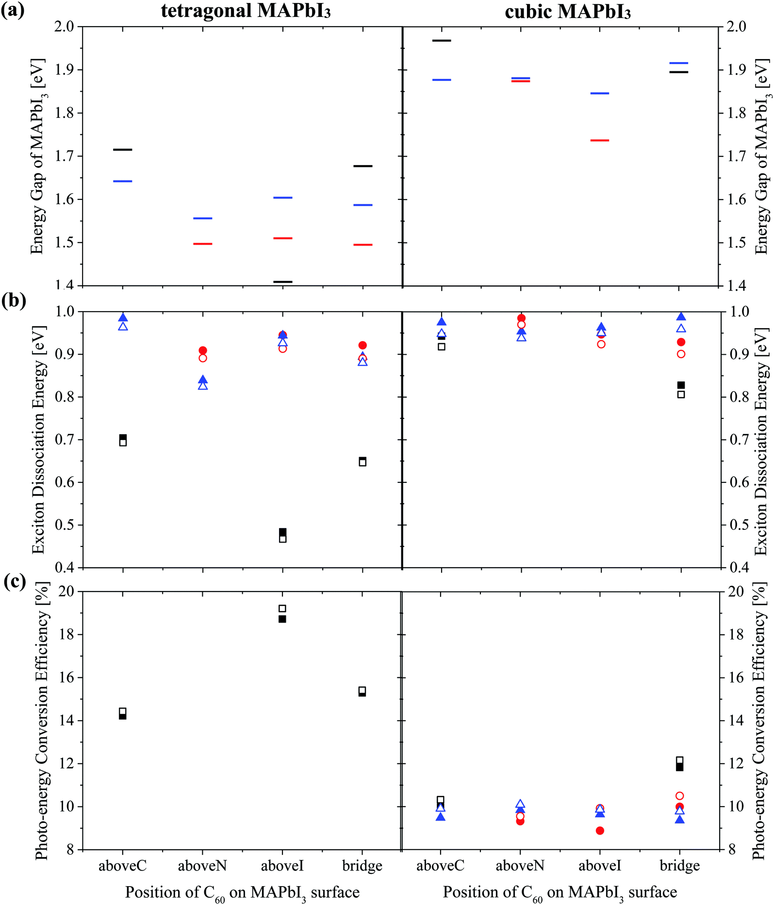 | ||
| Fig. 6 (a) Energy gap of MAPbI3Eg (b) exciton dissociation energy and (c) photo-energy conversion efficiency of a MAPbI3/C60 heterojunction for different C60 adsorbed sites based on Tables S2 and S3 (ESI†). Orientations of the MA cation with respect to the (001) surface are: topC (black), topN (red) and apolar (blue). Open symbols (Fig. S8(b) and(c), ESI†) represent the results obtained by taking the average value of the three-fold degenerate LUMO of C60 fullerene. | ||
Both the topN and apolar geometries have almost similar values of energy gap Eg and exciton dissociation energy ΔE. The electron-hole pair dissociation energy ΔE for the tetragonal MAPbI3 with the topC orientation is ∼0.48–0.70 eV, which is lower than that of the topN and apolar geometries ∼ 0.84–0.98 eV. Compared with the topN or apolar case, the topC geometry has a higher energy gap of Eg ∼ 1.7 eV and a smaller exciton dissociation energy of ΔE ∼ 0.7 eV. However, the topC case with C60 on the aboveI position is an exceptional case. It has the smallest exciton dissociation energy ΔE = 0.48 eV and the smallest energy gap of Eg = 1.41 eV.
The heterojunction with the topC orientation exhibits a high PCE of η > 14%. The PCE (η*) values calculated using the three-fold degenerate LUMO of C60 fullerene are 1–3% higher than η (ESI†). Among the t-MAI slab models with the topC orientation, the highest PCE of η ∼18.7% is realized when C60 is on the top of iodine or on the aboveI position. It has a higher efficiency of η* ∼ 19.2%, if the three-fold degenerate LUMO of C60 is considered. On the other hand, the tetragonal-phase heterojunction with topN and apolar orientations does not yield nonzero PCE, implying that charge transfer does not occur at the MAPbI3-C60 interface. Comparison to the heterojunction with tetragonal MAPbI3, the cubic-phase heterojunction has a larger exciton dissociation energy of ΔE > 0.8 eV and a higher energy gap of Eg > 1.7 eV, as summarized in Table S3 (ESI†). It is interesting to see that all the heterojunctions have a PCE of η ≥ 9%.
The interesting trends in the energy gap, the exciton dissociation energy, and the PCE in Fig. 6 can be understood by considering the effect of the surface electric dipole of MAPbI3, originating from the organic MA cation, as shown in Fig. 2. This polar MA cation can rotate at room temperature and the positive charge is localized around the NH3 group.68 Therefore, the topC geometry with the CH3 orienting towards the upper vacuum in all layers is favorable for the injection of photo-induced electrons into the LUMO of fullerene, as well as for the enhancement of the stability (as shown in Fig. 5(a)). The built-in electric field due to the inward pointing surface dipole of the MA cation of the topC geometry facilitates an oriented electron transport to fullerene and reduces charge recombination. For the particular case of the aboveI configuration, the separation of photogenerated electron–hole pairs is significantly enhanced by taking the advantage of electronegativity of iodine. Therefore, it has the lowest exciton dissociation energy of ΔE ∼ 0.5 eV and the highest PCE of η ∼ 19%. For the topN geometry, the outward pointing surface dipole leads to an internal field that reduces the stability of the MAPbI3/C60 heterojunction, as shown in Fig. 5(a). For the cubic MAPbI3, one interesting feature, which can be seen from Fig. 6, is that the HOMO–LUMO gap of MAPbI3Eg, the exciton dissociation energy ΔE, and the PCE do not have an obvious dependence on the orientation of MAI and the location of C60 on the MAPbI3 surface. This is attributed to the relatively weak polar behavior (and therefore, the built-in electric field) of the cubic MAPbI3 as compared to the tetragonal phase.
In the present study, our predicted PCE values are comparable to the reported values of ∼20% for the HTM-free PSC based on a MAPbI3 with F4TCNQ molecules as the electron acceptor.38 Cojocaru et al. studied the effect of temperature on the PCE of MAPbI3 with both HTM and ETM layers.69 They reported a PCE of η ∼ 14% at temperature T ∼ 30 °C, and the efficiency decreases to η ∼ 5% at T > 55 °C. The performance decline of perovskite solar cells is also reported experimentally by Schwenzer et al.70 Our calculations show that the tetragonal MAPbI3/C60 heterojunction with the C60 on the aboveC position of the topC MAPbI3 surface has the highest PCE of η ∼ 19%, whereas the PCE of the heterojunction decreases to η ∼ 10% for the case of a high-temperature cubic MAPbI3. Since we consider only one C60 on a MAPbI3 surface of 2 × 2 periodicity in-plane, the predicted PCE could be higher if a full coverage of C60 on the MAPbI3 surface is performed. The present GGA-PBE calculation predicts bandgap values of MAPbI3 surfaces that agree reasonably well with the experiments, as discussed earlier. This is due to the fortuitous cancellation of the GGA underestimated gap and the lack of the electron–hole coupling of exciton, which overestimates the optical gap.66 Nevertheless, our calculated PCE values may not be accurate due to the use of GGA-PBE eigenvalues for Eg and ΔE, although they will give a rough estimation.
5 Conclusions
In summary, we have performed first-principles DFT calculations on the photo-energy conversion efficiency (PCE) of MAPbI3/C60 heterojunctions. Finite slab models of both tetragonal and cubic MAPbI3(001) surfaces with MAI terminations are considered. A fullerene C60 is introduced to different positions of the MAPbI3 surface. Our studies reveal that the stability, the exciton dissociation efficiency, and the PCE of the heterojunction with the tetragonal MAPbI3 strongly depend on the nature of the MAPbI3 surfaces. The MAPbI3/C60 heterojunction with CH3 of the MA cation orienting towards the upper vacuum in all layers is energetically more stable than the MAPbI3 with the CH3 orienting towards the upper vacuum in all layers (the topN geometry), or the MAPbI3 with half of the MA cations having their –NH3 or –CH3 groups pointing up (and half pointing down) (the apolar geometry). In this case, the built-in field forms from the inward pointing the surface electric dipole of the MA cations of the topC geometry promoting the electron transfer to fullerene and suppressing charge recombination, implying an electric–dipole aided charge separation. The recent experimental observations of the enhancement of PCE in the MAPbI3 solar cells by coupling the perovskites with ferroelectrics or by applying an electrical poling further support the importance of this phenomenon.71,72 Recently, Yu et al. studied the effect of Lewis base and graphene on the performance of MAPbI3 solar cells.73 Their study demonstrates the important role of the interface dipole in the improved performance of PSCs by facilitating the electron extraction via graphene. The separation of photogenerated electron–hole pairs is further enhanced when C60 is located directly on the top of iodine. We find that the functionalization of topC-MAPbI3 with a fullerene can achieve a high PCE of η > 14%, and the highest efficiency of η ∼19% can be achieved when the fullerene is located directly on the top of iodine. However, a drawback is that this heterojunction can harvest light and convert to energy only if the fullerene (or an electron transport material) is located on MAPbI3 with the topC geometry, but not the topN or apolar geometry. A fullerene absorbed on a cubic MAPbI3 surface gives a lower PCE of η ∼10%, although the stability and PCE do not sensitively depend on the MA orientation and the C60 position on the MAPbI3 surface.Conflicts of interest
There are no conflicts of interest to declare.Acknowledgements
This work has been supported by the Institute for Materials Research (IMR), Tohoku University and Dassault Systèmes BIOVIA for the use of supercomputer facilities of IMR and for the ambassador license of BIOVIA. KHChew acknowledges the support from the Air Force Office of Scientific Research under award number FA2386-20-1-4011.References
- A. K. Jena, A. Kulkarmi and T. Miyasaka, Chem. Rev., 2019, 119, 3036–3103 CrossRef CAS.
- A. Kojima, K. Teshima, Y. Shirai and T. Miyasaka, J. Am. Chem. Soc., 2009, 131, 6050–6051 CrossRef CAS.
- M. M. Lee, J. Teuscher, T. Miyasaka, T. N. Murakami and H. J. Snaith, Science, 2012, 338, 643–647 CrossRef CAS.
- W. S. Yang, J. H. Noh, N. J. Jeon, Y. C. Kim, S. Ryu, J. Seo and S. I. Seok, Science, 2015, 348, 1234–1237 CrossRef CAS.
- M. A. Green, E. D. Dunlop, J. Hohl-Ebinger, M. Yoshita, N. Kopidakis and X. Hao, Prog. Photovoltaics, 2020, 28, 629–638 Search PubMed.
- S. Chen, Y. Hou, H. Chen, M. Richter, F. Guo, S. Kahmann, X. Tang, T. Stubhan, H. Zhang, N. Li, N. Gasparini, C. O. R. Quiroz, L. S. Khanzada, G. J. Matt, A. Osvet and C. J. Brabec, Adv. Energy Mater, 2016, 6, 1600132 CrossRef.
- W. Yang, Y. Yao and C.-Q. Wu, J. Appl. Phys., 2015, 117, 095502 CrossRef.
- Y. Zhou and A. A. Gray-Weale, Phys. Chem. Chem. Phys., 2016, 18, 4476–4486 RSC.
- Y. Zhou and G. Long, J. Phys. Chem. C, 2017, 121, 1455–1462 CrossRef CAS.
- A. Poglitsch and D. Weber, J. Chem. Phys., 1987, 87, 6373–6378 CrossRef CAS.
- H. Gaonkar, J. Zhu, R. Kottokkaran, B. Bhageri, M. Noack and V. Dalal, ACS Appl. Energy Mater., 2020, 3, 3497–3503 CrossRef CAS.
- G. Yu, J. Gao, J. C. Hummelen, F. Wudi and A. J. Heeger, Science, 1995, 270, 1789 CrossRef CAS.
- P. Peumans, A. Yakimov and S. R. Forrest, J. Appl. Phys., 2003, 93, 3693 CrossRef CAS.
- J. Drechsel, B. Männig, F. Kozlowski, M. Pfeiffer and K. Leo, Appl. Phys. Lett., 2005, 86, 244102 CrossRef.
- Y. Kodama and K. Ohno, Appl. Phys. Lett., 2010, 96, 034101 CrossRef.
- S. Ono, R. Kuwahara and K. Ohno, J. Appl. Phys., 2014, 116, 054305 CrossRef.
- Y. Fang, C. Bi, D. Wang and J. Huang, ACS Energy Lett., 2017, 2, 782–794 CrossRef CAS.
- T. Gatti, E. Menna, M. Meneghetti, M. Maggini, A. Petrozza and F. Lamberti, Nano Energy, 2017, 41, 84–100 CrossRef CAS.
- J. Pascual, J. L. Delgado and R. Tena-Zaera, J. Phys. Chem. Lett., 2018, 9, 2893–2902 CrossRef CAS.
- E. Castro, J. Murillo, O. Fernandez-Delgado and L. Echegoyen, J. Mater. Chem. C, 2018, 6, 2635–2651 RSC.
- Y. Shao, Z. Xiao, C. Bi, Y. Yuan and J. Huang, Nat. Commun., 2014, 5, 5784 CrossRef CAS.
- J. Xu, A. Buin, A. H. Ip, W. Li, O. Voznyy, R. Comin, M. Yuan, S. Jeon, Z. Ning, J. J. McDowell, P. Kanjanaboos, J. P. Sun, X. Lan, L. N. Quan, D. H. Kim, I. G. Hill, P. Maksymovych and E. H. Sargent, Nat. Commun., 2015, 6, 7081 CrossRef CAS.
- J.-Y. Jeng, Y.-F. Chiang, M.-H. Lee, S.-R. Peng, T.-F. Guo, P. Chen and T.-C. Wen, Adv. Mater., 2013, 25, 3727–3732 CrossRef CAS.
- X. Zheng, B. Chen, J. Dai, Y. Fang, Y. Bai, Y. Lin, H. Wei, X. C. Zeng and J. Huang, Nat. Energy, 2017, 2, 17102 CrossRef CAS.
- H. Rao, S. Ye, W. Sun, W. Yan, Y. Li, H. Peng, Z. Liu, Z. Bian, Y. Li and C. A. Huang, Nano Energy, 2016, 27, 51–57 CrossRef CAS.
- H. Yoon, S. M. Kang, J.-K. Lee and M. Choi, Energy Environ. Sci., 2016, 9, 2262–2266 RSC.
- K.-M. Lee, C.-C. Chen, L.-C. Chen, S. H. Chang, K.-S. Chen, S.-C. Yeh, C.-T. Chen and C.-G. Wu, Sol. Energy Mater. Sol. Cells, 2017, 164, 13–18 CrossRef CAS.
- D. Liu, Q. Wang, C. J. Traverse, C. Yang, M. Young, P. S. Kuttipillai, S. Y. Lunt, T. W. Hamann and R. R. Lunt, ACS Nano, 2018, 12, 876–883 CrossRef CAS.
- Z. Song, A. Abate, S. C. Watthage, G. K. Liyanage, A. B. Phillips, U. Steiner, M. Graetzel and M. J. Heben, Adv. Energy Mater., 2016, 6, 1600846 CrossRef.
- Y. Han, S. Meyer, Y. Dkhissi, K. Weber, J. M. Pringle, U. Bach, L. Spiccia and Y.-B. Cheng, J. Mater. Chem. A, 2015, 3, 8139–8147 RSC.
- M. I. Saidaminov, J. Kim, A. Jain, R. Quintero-Bermudez, H. Tan, G. Long, F. Tan, A. Johnston, Y. Zhao, O. Voznyy and E. H. Sargent, Nat. Energy, 2018, 3, 648–654 CrossRef CAS.
- H. S. Kim, C. R. Lee, J. H. Im, K. B. Lee, T. Moehl, A. Marchioro, S.-J. Moon, H.-B. Robin, J.-H. Yum, J. E. Moser, M. Grätzel and N.-G. Park, Sci. Rep., 2012, 2, 591 CrossRef.
- R. S. Sanchez and E. Mas-Marza, Sol. Energy Mater. Sol. Cells, 2016, 158, 189–194 CrossRef CAS.
- K. Domanski, J.-P. Correa-Baena, N. Mine, M. K. Nazeeruddin, A. Abate, M. Saliba, W. Tress, A. Hagfeldt and M. Grätzel, ACS Nano, 2016, 10, 6306–6314 CrossRef CAS.
- A. K. Jena, Y. Numata, M. Ikegami and T. Miyasaka, J. Mater. Chem. A, 2018, 6, 2219–2230 RSC.
- L. Etgar, P. Gao, Z. Xue, Q. Peng, A. K. Chandiran, B. Liu, M. K. Nazeeruddin and M. Grätzel, J. Am. Chem. Soc., 2012, 134, 17396–17399 CrossRef CAS.
- H. Chen and S. Yang, Adv. Mater., 2017, 29, 1603994 CrossRef.
- W.-Q. Wu, Q. Wang, Y. Fang, Y. Shao, S. Tang, Y. Deng, H. Lu, Y. Liu, T. Li, Z. Yang, A. Gruverman and J. Huang, Nat. Commun., 2018, 9, 1625 CrossRef.
- S. Yun, X. Zhou, J. Even and A. Hagfeldt, Angew. Chem., Int. Ed., 2017, 56, 15806–15817 CrossRef CAS.
- X. Zhou, J. Jankowska, H. Dong and O. V. Prezhdo, J. Energy Chem., 2018, 27, 637–649 CrossRef.
- C.-J. Yu, J. Phys. Energy, 2019, 1, 022001 CrossRef CAS.
- J. Yin, D. Cortecchia, A. Krishna, S. Chen, N. Mathews, A. C. Grimsdale and C. Soci, J. Phys. Chem. Lett., 2015, 6, 1396–1402 CrossRef CAS.
- C. Quarti, F. D. Angelis and D. Beljonne, Chem. Mater., 2017, 29, 958–968 CrossRef CAS.
- W. Shockley and H. J. Queisser, J. Appl. Phys., 1961, 32, 510 CrossRef CAS.
- K. Seki, A. Furube and Y. Yoshida, Appl. Phys. Lett., 2013, 103, 253904 CrossRef.
- M. I. Hossain, W. Qarony, S. Ma, L. Zeng, D. Knipp and Y. H. Tsang, Nano-Micro Lett., 2019, 11, 58 CrossRef CAS.
- Refer https://rredc.nrel.gov/solar//spectra/am1.5/for Reference Solar Spectral Irradiance: Air Mass 1.5.
- B. Delley, J. Chem. Phys., 1990, 92, 508–517 CrossRef CAS.
- B. Delley, J. Chem. Phys., 2000, 113, 7756–7764 CrossRef CAS.
- B. Delley, Modern Density Functional Theory: A Tool for Chemistry in Theoretical and Computational Chemistry, Elservier, ed. J. M. Seminario and P. Politzer, 1995, vol. 2 Search PubMed.
- E. R. McNellis, J. Meyer and K. Reuter, Phys. Rev. B: Condens. Matter Mater. Phys., 2009, 80, 205414 CrossRef.
- A. Tkatchenko and M. Scheffler, Phys. Rev. Lett., 2009, 102, 073005 CrossRef.
- C. Motta, F. El-Mellouhi, S. Kais, N. Tabet, F. Alharbi and S. Sanvito, Nat. Commun., 2015, 6, 7026 CrossRef CAS.
- J. P. Perdew, K. Burke and M. Ernzerhof, Phys. Rev. Lett., 1996, 77, 3865–3868 CrossRef CAS.
- W.-J. Yin, T. Shi and Y. Yan, J. Phys. Chem. C, 2015, 119, 5253–5264 CrossRef CAS.
- R. A. Jishi, O. B. Ta and A. A. Sharif, J. Phys. Chem. C, 2014, 118, 28344–28349 CrossRef CAS.
- W. Geng, L. Zhang, Y.-N. Zhang, W.-M. Lau and L.-M. Liu, J. Phys. Chem. C, 2014, 118, 19565–19571 CrossRef CAS.
- A. M. A. Leguy, J. M. Frost, A. P. McMahon, V. G. Sakai, W. Kockelmann, C. Law, X. Li, F. Foglia, A. Walsh, B. C. O’Regan, J. Nelson, J. T. Cabral and P. R. F. Barnes, Nat. Commun., 2015, 6, 7124 CrossRef.
- T. Baikie, N. S. Barrow, Y. Fang, P. J. Keenan, P. R. Slater, R. O. Piltz, M. Gutmann, S. G. Mhaisalkar and T. J. White, J. Mater. Chem. A, 2015, 3, 9298–9307 RSC.
- Y. Kawamura, H. Mashiyama and K. Hasebe, J. Phys. Soc. Jpn., 2002, 71, 1694–1697 CrossRef CAS.
- W.-J. Yin, J.-H. Yang, J. Kang, Y. Yan and S.-H. Wei, J. Mater. Chem. A, 2015, 3, 8926–8942 RSC.
- F. Brivio, K. T. Butlet, A. Walsh and M. Van Schilfgaarde, Phys. Rev. B: Condens. Matter Mater. Phys., 2014, 89, 155204 CrossRef.
- T. Ahmed, C. La-O-Varakiat, T. Salim, Y. M. Lam, E. E. M. Chia and J.-X. Zhu, EPL, 2014, 108, 67015 CrossRef.
- Y. Yamada, T. Nakamura, M. Endo, A. Wakamiya and Y. Kanemitsu, Appl. Phys. Express, 2014, 7, 032302 CrossRef.
- V. D’Innocenzo, G. Grancini, M. J. P. Alcocer, A. R. S. Kandada, S. D. Stranks, M. M. Lee, G. Lanzani, H. J. Snaith and A. Petrozza, Nat. Commun., 2014, 5, 3586 CrossRef.
- E. Mosconi, A. Amat, M. K. Nazeeruddin, M. Grätzel and F. D. Angelis, J. Phys. Chem. C, 2013, 117, 13902–13913 CrossRef CAS.
- Y. Inada and H. Orita, J. Comput. Chem., 2008, 29, 225–232 CrossRef CAS.
- A. Stroppa, C. Quarti, F. D. Angelis and S. Picozzi, J. Phys. Chem. Lett., 2015, 6, 2223–2231 CrossRef CAS.
- L. Cojocaru, S. Uchida, Y. Sanehira, V. Gonzalez-Pedro, J. Bisquert, J. Nakazaki, T. Kubo and H. Segawa, Chem. Lett., 2015, 44, 1750–1752 CrossRef CAS.
- J. A. Schwenzer, L. Rakocevic, R. Gehlhaar, T. Abzieher, S. Gharibzadeh, S. Maghadamzadeh, A. Quintilla, B. S. Richards, U. Lemmer and U. W. Paetzold, ACS Appl. Mater. Interfaces, 2018, 10, 16390–16399 CrossRef CAS.
- E. Jia, D. Wei, P. Cui, J. Ji, H. Huang, H. Jiang, S. Dou, M. Li, C. Zhou and W. Wang, Adv. Sci., 2019, 6, 1900252 CrossRef.
- A. Bruno, D. Cortecchia, X. Y. Chin, K. Fu, P. P. Boix, S. Mhaisalkar and C. Soci, Adv. Energy Mater., 2017, 1700265 CrossRef.
- C.-J. Yu, Y.-H. Kye, U.-G. Jong, K.-C. Ri, S.-H. Choe, J.-S. Kim, S.-G. Ko, G.-I. Ryu and B. Kim, ACS Appl. Mater. Interfaces, 2020, 12, 1858–1866 CrossRef CAS.
Footnote |
| † Electronic supplementary information (ESI) available. See DOI: 10.1039/d0ma00853b |
| This journal is © The Royal Society of Chemistry 2021 |