DOI:
10.1039/D0MA00751J
(Paper)
Mater. Adv., 2021,
2, 718-727
Enhancement of electromagnetic interference shielding from the synergism between Cu@Ni nanorods and carbon materials in flexible composite films†
Received
30th September 2020
, Accepted 3rd December 2020
First published on 8th December 2020
Abstract
A series of composite films containing poly(vinylidene fluoride) (PVDF), carbon nanotubes (CNTs), graphene and bimetallic nanorods, in which copper was wrapped with nickel (Cu@Ni), were fabricated via a facile preparation method of solution casting and compression molding. The electrical conductivity, thermal conductivity, and electromagnetic interference shielding effectiveness of the PVDF/CNT/graphene/Cu@Ni composite films were adjusted by varying the Cu@Ni content. A stronger EMI shielding performance (158.8 dB mm−1) was achieved due to the synergistic effects between Cu@Ni nanorods and carbonaceous nanofillers (CNTs and graphene) compared with our previous studies. The Cu@Ni nanorods particularly contributed both magnetic loss and dielectric loss to the electromagnetic wave. The increased electrical and thermal conductivity with Cu@Ni content facilitated the films’ ability to transform electromagnetic wave energy into Joule heat. Moreover, the composite films possessed enhanced mechanical strength, flexibility and electrical stability due to the ordered filler network between the PVDF and the fillers.
1. Introduction
Rapid development in telecommunications and electronic interfaces has given rise to significant levels of hazardous electromagnetic interference (EMI), which can degrade the performance and decrease the lifetime of electronic components. Therefore, EMI shielding materials are required to prevent the penetration of harmful EM waves into electronic components, thus facilitating the environment protection and human health.1 Traditional metallic shielding materials are popular but may be restricted due to their disadvantages of overweight, susceptibility to corrosion, deforming difficulty, and potential production of secondary electromagnetic (EM) pollution. In order to overcome these drawbacks, conductive polymer composites (CPCs), made from a polymer matrix and conductive fillers, which are light, resistant to corrosion and easy to manufacture2 are being cited increasingly as potential materials for attenuating EM waves. The EMI shielding performance of CPCs is mainly dependent on the characteristics of nanofillers including electrical/thermal conductivity, magnetic/dielectric properties, aspect ratio, dispersity and physical geometry.1
As a consequence, the technology behind the nanofillers employed in CPCs, such as nanotubes,3,4 nanowires,5–7 nanorods,8 graphene,9,10 MXene,11,12 black phosphorus,13 and transition metal dichalcogenides,14 has greatly promoted the development of the EMI shielding performance. Carbonaceous nanofillers such as carbon nanotubes (CNTs) and graphene have a controllable aspect ratio and are of great flexibility, lightweight, oxidation-resistant, and highly thermally and electrically conductive.15 Additionally, CNT/graphene composites are particularly interesting as they could fulfill the full band absorption in a range of 2–18 GHz.16 They are therefore considered beneficial for the development of the EMI shielding technology.
Based on the EMI shielding mechanisms of reflection and absorption, conductive carbon materials or composites containing carbonaceous nanofillers can reflect the incident EM waves by an impedance mismatch. The downside to the reflection is that it produces secondary EM pollution. On the other hand, charge carriers or magnetic/electric dipoles of the magnetic or EM components are able to attenuate the EM waves via absorption loss, which is dependent on the dielectric and magnetic loss ability of CPCs. As a result, ferromagnetic nanofillers such as Ni,17–20 Fe,21–23 and Co24,25 in composites have a strong absorption performance, but there is a tradeoff with a higher filler content and a greater thickness of EMI shielding materials. Accordingly, incorporation of nanofillers is favorable to accumulate each single fundamental property in a solitaire composite for promoting the EMI shielding performance.26 Based on our previous studies on ternary-phase CPCs containing CNT/graphene27,28 and monometallic Ni,29 the conduction and dielectric loss could be achieved from carbonaceous nanofillers,30 while magnetic loss could be primarily introduced from magnetic ferrites and metals. Therefore, CPCs containing magnetic metals and carbonaceous nanofillers, correspondingly acting as a metal–carbon ternary or quaternary phase composite, can be realistic EMI shielding materials because of the combination of the magnetic loss (magnetic domain movement, spin resonance and relaxation of magnetization) and conduction loss (Ohmic loss and dielectric conductivity loss).31
Compared with monometallic magnetic metals, bimetallic alloys such as Fe–Ni,32,33 Co–Ni,31,34 Co–Fe35 and sendust–Ag36 showed complementary effects in balancing the complex relative permittivity and permeability due to their dielectric–magnetic loss ability. Additionally, copper exhibits excellent mechanical, thermal and electrical properties, but when exposed to air it has a great tendency to be oxidized.37 Therefore, introducing a magnetic nickel shell wrapped on the copper core not only improves the magnetic loss ability of the hybrid but also prevents its oxidation. In our previous study, the Ni–Cu alloy was found to have high impedance match, dielectric loss, multiple polarization relaxation and natural resonance in favor of attenuation of EMI waves.38 It particularly exhibited a strong absorption loss by balancing the dielectric and magnetic losses when anchored on reduced graphene oxide (rGO).39 Noticeably, high magnetic magnetization alloys may exhibit poor impedance matching ability due to their ultrahigh conductivity.36,40 As a result, there are still open issues on the synergistic effects between the Ni–Cu alloy and the carbonaceous nanofillers in CPCs, despite the metal–carbon structures and the bimetallic alloys being reported to be efficient for attenuating EM waves.
Herein, composite films were fabricated with 1-dimensional (1-D) Cu@Ni nanorods that had a core–shell microstructure as an adjustable nanofiller, and was reinforced by CNT/graphene. Poly(vinylidene fluoride) (PVDF) was selected as the polymer matrix because of its pyroelectric effect, substantial dielectric constant, high mechanical stiffness, thermal solidity and processability. Then, this study investigated the EMI shielding effectiveness (SE), electrical conductivity (EC), thermal conductivity (TC), and mechanical strength of the fabricated PVDF/CNT/graphene/Cu@Ni composite films by varying the Cu@Ni content. Compared with the EMI shielding carbon CPCs in the literature, the Cu@Ni-decorated composite films possessed a strong performance in terms of their high EMI shielding performance with a thin structure. Furthermore, the increase in TC prompted the composite films to absorb microwave energy and quickly dissipate the converted Joule heat, which are in favor of the film's ability to protect sensitive electronic instruments.
2. Experimental
2.1 Raw materials
Copper(II) nitrate trihydrate (Cu(NO3)2·3H2O) was provided from Tianjin Kemiou Chemical Reagent Co., Ltd (Tianjin, China). Nickel(II) nitrate hexahydrate (Ni(NO3)2·6H2O), sodium hydrate (NaOH), and ethylenediamine (H2NCH2CH2NH2, EDA) were purchased from Tianjin Fengchuan Chemical Reagent Technologies Co., Ltd (Tianjin, China). Hydrazine hydrate (N2H4·H2O) was acquired from Tianjin Fuyu Fine Chemical Co., Ltd (Tianjin, China). Graphene nanoplates were supplied by NanoXplore, Inc. Multi-walled carbon nanotubes (NC7000) were supplied by Nanocyl SA. They had an average diameter of 9 nm and a length of approximately 1.5 μm. Poly(vinylidene fluoride) was purchased from Solvay with a grade of Solef® 6020. All reagents were of analytical grade and were used as received without further purification.
2.2 Synthesis procedure of core–shell Cu@Ni nanorods
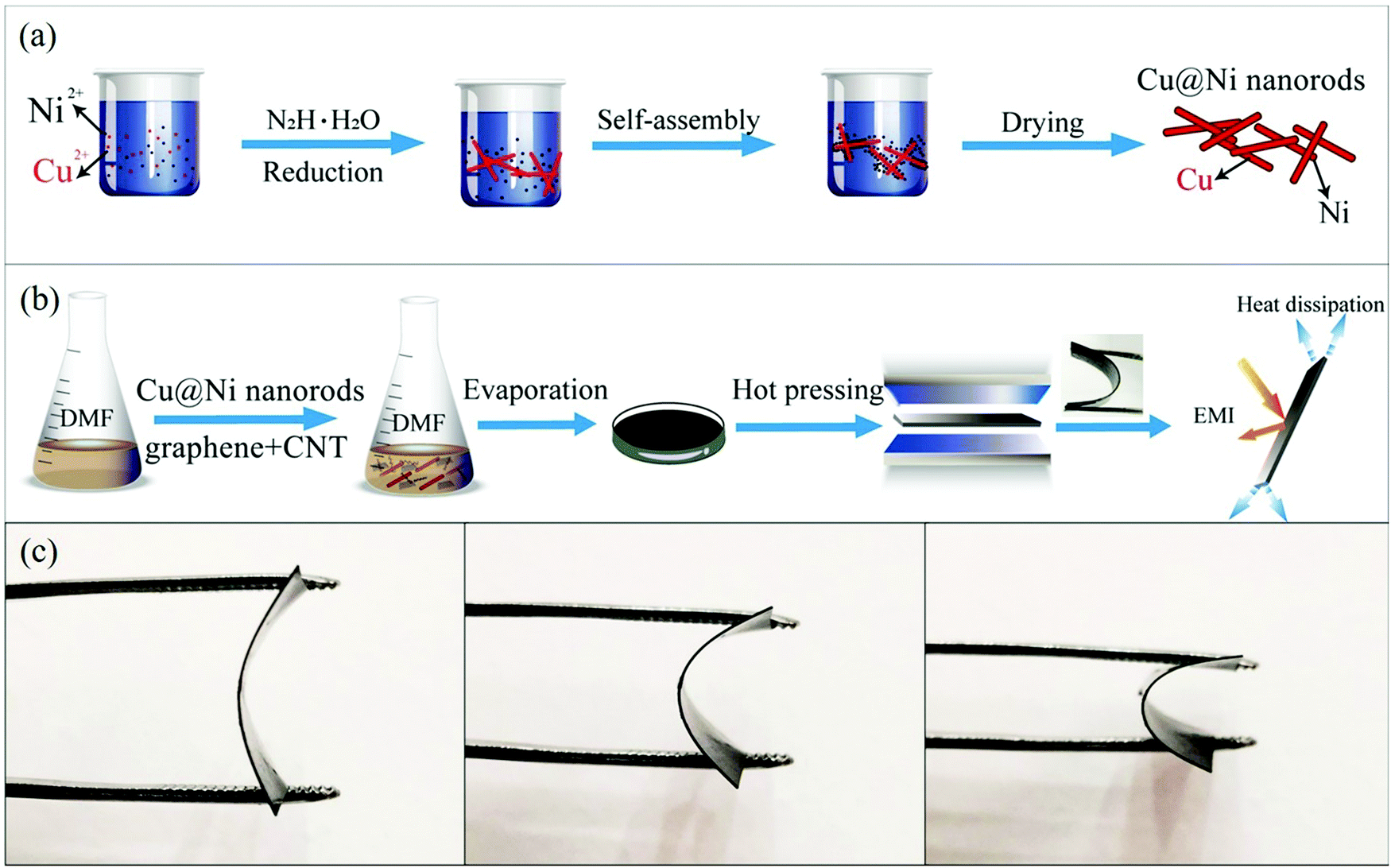
The preparation process of the Cu@Ni nanorods is illustrated schematically in Fig. 1(a). Initially, 0.2 mL of Cu(NO3)2·3H2O (0.5 mol L−1) and 0.2 mL of Ni(NO3)2·6H2O (0.5 mol L−1) were dissolved in a plastic reactor containing 60 mL of highly concentrated NaOH (7.0 M). This solution was then stirred for 15 min. 0.1 mL of EDA was added, and this solution was stirred until it became turbid. 0.05 mL of N2H4·H2O was added to this turbid solution, and it was stirred for 7 minutes. The reactor was kept at 80 °C for 1 hour and then allowed to drop to ambient temperature via natural cooling. Finally, the liquid was centrifuged, and washed multiple times using ethanol and distilled water, and then vacuum dried at 50 °C to obtain the final Cu@Ni samples.
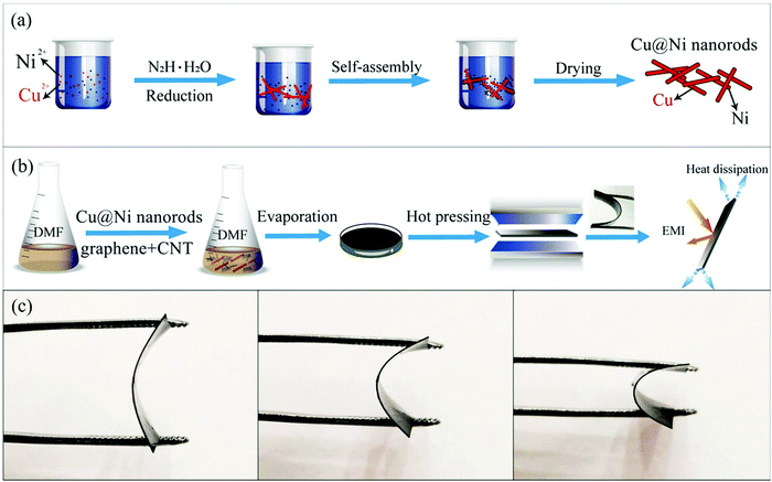 |
| | Fig. 1 Schematic illustration of the fabrication process of (a) Cu@Ni nanorods and (b) the PVDF/CNT/graphene/Cu@Ni composite film and (c) the digital image of the bent composite film with 8 wt% Cu@Nis. | |
2.3 Fabrication procedure of PVDF/CNT/graphene/Cu@Ni composite films
PVDF/CNT/graphene/Cu@Ni composite films were fabricated via solution mixing and compression molding (Fig. 1(b)). After PVDF was dissolved in dimethyl formamide (DMF) solution at 60 °C, 0.6 g of CNTs and 0.8 g of graphene were then stirred into the prepared PVDF/DMF solution. When the homogeneous PVDF/CNT/graphene solution was prepared, different amounts of Cu@Ni nanorods were dispersed in the solution via the ultrasonication method. Lastly, the PVDF/CNT/graphene/Cu@Ni composite film was obtained from its evaporated solution in a vacuum oven at 60 °C for 5 hours. Compression molding at 190 °C and 15 MPa was used to produce a 30 mm diameter circle of the 0.3 mm thick film. A series of composite films containing 6 wt% CNT, 8 wt% graphene, and different Cu@Ni contents of 0.6 wt%, 1.2 wt%, 2 wt%, 4 wt%, 6 wt%, and 8 wt% were fabricated. The amount of PVDF and Cu@Ni in DMF is listed in Table S1 in the ESI.† As shown in Fig. 1(c), the composite film has a high degree of flexibility and can be repeatedly bent.
2.4 Characterization
The details of structural characterization, including the wide-angle X-ray diffraction (XRD) pattern tests and the field-emission scanning electron microscopy (FE-SEM) observations, as well as the EMI SE, EC and TC measurements, were described in our previous papers.24,29 Additionally, the values of EMI SE, including total SE (SET), reflection SE (SER) and absorption SE (SEA), were obtained from applying eqn (1)–(6):26,41| | | A = 1 − |S11|2 − |S12|2 | (3) |
| | SER = −10![[thin space (1/6-em)]](https://www.rsc.org/images/entities/char_2009.gif) log(1 − R) log(1 − R) | (4) |
| | 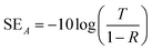 | (5) |
where S11 and S21 are the scattering parameters.
Dynamic mechanical analysis of the composite films was performed with a dynamic mechanical analyzer (DMA mode 450, 01db-Metravib, France) in the double cantilever mode at a constant frequency of 1 Hz, a static force of 0.01 N, a strain amplitude of 10 μm, a temperature range of 20 °C to 150 °C, and a scan rate of 3 °C min−1. The elastic modulus of the composite films was measured using a nano-indenter (DSI, KLA-Tencor) from the maximum peak value of the relevant displacement curve.
3. Results and discussion
3.1 Structure characterization of PVDF/CNT/Cu@Ni composite films
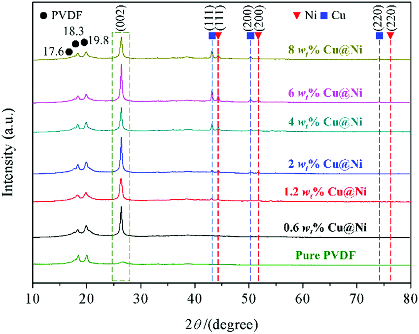
Fig. 2 shows the XRD patterns of the PVDF/CNT/graphene/Cu@Ni composite films with different Cu@Ni contents, while a detailed XRD pattern of Cu@Ni is shown in Fig. S1(a) in the ESI.† As shown in Fig. 2, four identical diffraction peaks at 2θ = 17.6°, 18.3°, 19.8°, and 26.5° are assigned to the diffraction peaks (100), (020), (110), and (021) of the PVDF α-phase crystal.42 There is no evidence to support the transformation from the α phase to the β phase in the PVDF. Compared with the pure PVDF spectrum,24 the diffraction peaks of the Ni and Cu crystals were observed when the Cu@Ni contents exceeded 4 wt%. The XRD patterns of the composite films at 2θ = 44.5°, 51.8° and 76.4°, as well as those at 2θ = 43.3°, 50.4° and 74.2°, correspond to the face-centered cubic (111), (200) and (220) crystal faces of Ni and Cu, respectively.38 These diffraction peaks are assigned to the Cu and Ni based on the standard Joint Committee on Powder Diffraction Standards card of copper and nickel (PDF#04-0836 and PDF#04-0850),43 and the peaks indicate a mixture of Cu and Ni metals in Cu@Ni. Additionally, the intensity of the Ni and Cu peaks increased with the Cu@Ni contents due to the different standard reduction potentials of the Ni and Cu atoms.38 No other characteristic peaks are observed, demonstrating that the Cu@Ni nanorods were not oxidized during the synthesis and the film fabrication process, thus confirming the existence of the pure phase of Cu@Ni. In addition to Cu and Ni, the diffraction peak of the (002) plane at 2θ = 26° as shown in Fig. 2, which corresponds to the graphite structure,44,45 is close to that of the (021) plane at 2θ = 26.5°,46,47 and thus the (021) and (002) planes cannot be distinguished explicitly.
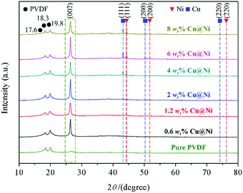 |
| | Fig. 2 XRD patterns of the PVDF/CNT/graphene/Cu@Ni composite films. | |
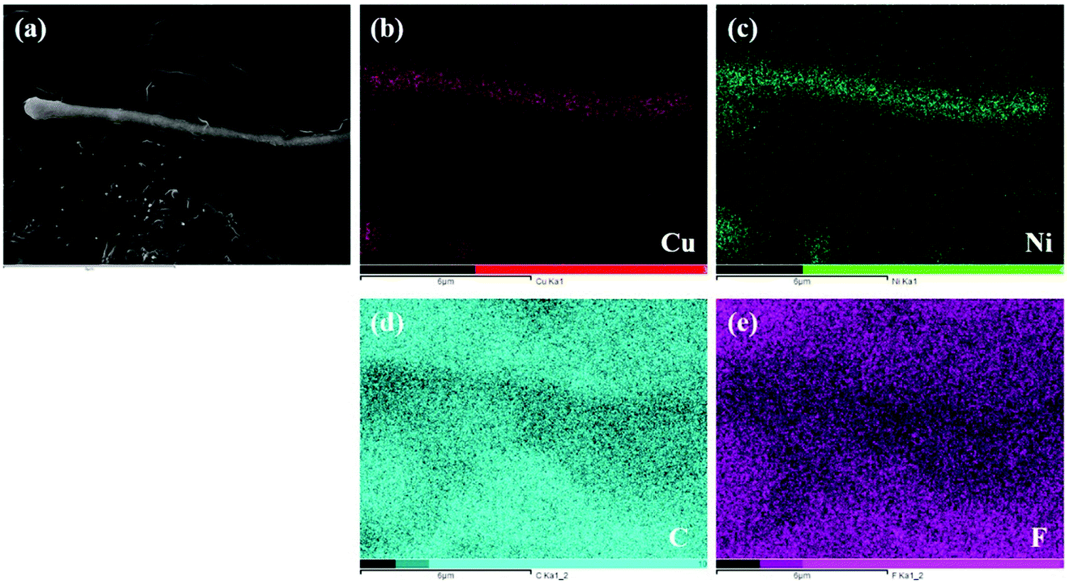
Fig. 3 shows the elemental mapping images of the PVDF/CNT/graphene/Cu@Ni composite films, which identifies the co-existence of the Cu and Ni elements in Cu@Ni; the C element in PVDF, CNT and graphene; and the F element in PVDF in the composite film. Therefore, the results from XRD and elemental mapping confirm that the Cu@Ni, graphene and CNTs were dispersed sufficiently throughout the PVDF. Additionally, a 1-D rod structure Cu@Ni is demonstrated because the Cu and Ni elements are concentrated in the shape of a rod as shown in Fig. 3(b) and (c), whereas the C and F elements are dispersed throughout the whole section as shown in Fig. 3(d) and (e). Furthermore, the element mapping of the Ni element is wider than that of Cu, which implies that the Ni shell covers the Cu core. This core–shell structure was induced by the different standard reduction potentials of copper [E0 (Cu2+/Cu0) = 0.342 V] and nickel [E0 (Ni2+/Ni0) = −0.257 V]. The higher potential facilitated Cu to be reduced in the competitive redox reactions and acted as a nucleation precursor, while Ni2+ ions were reduced in situ to coat on the Cu surface.48,49 Therefore, hybrid nanorods, in which Cu was wrapped with Ni, were prepared.
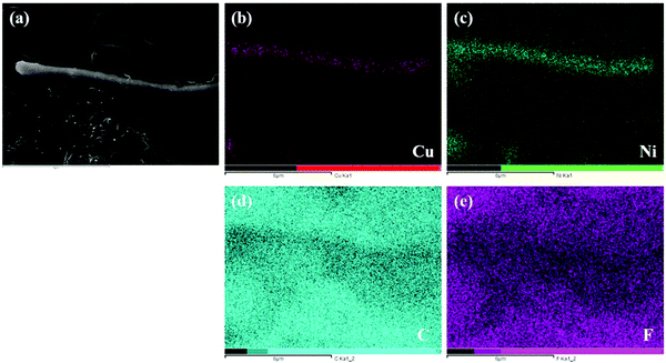 |
| | Fig. 3 SEM image (a) and elemental mapping images of ((b) Cu, (c) Ni, (d) C and (e) F) of the PVDF/CNT/graphene/Cu@Ni composite films. | |
A conducting network is formed when the fillers are introduced into the polymer matrix and they are contacted with each other. This constructed network, providing continuous paths for phonon and electron migration, is the primary issue for the high electrical and thermal transfer in CPCs.50 Therefore, the morphologies of the prepared Cu@Ni nanorods were observed in the FE-SEM images. The overall perspective of the Cu@Ni nanorods in Fig. S1(b) and (c) (ESI†) shows a rod structure with an average diameter of 0.3 μm and a length of 5–10 μm. Additionally, the cross-sections of the PVDF/CNT/graphene/Cu@Ni composite films in Fig. 4 show a uniform distribution of the CNTs, graphene, and Cu@Ni nanorods in the PVDF matrix. The Cu@Ni nanorods are found to co-exist with the CNTs and graphene, and the Cu@Ni nanorods in the FE-SEM images are observed to become increasingly concentrated with the Cu@Ni content being increased. This signifies an enhancement on the bridge effect between the fillers. Moreover, the CNTs, graphene, and Cu@Ni show rare signs of detachment from the PVDF. Additionally, the 1-D structure of the Cu@Ni nanorods with a high aspect ratio is favorable to avoid the aggregation of graphene and CNTs.6
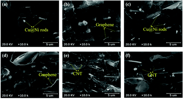 |
| | Fig. 4 SEM images of PVDF/CNT/graphene/Cu@Ni composite films with different CNT contents: (a) 0.6 wt%, (b) 1.2 wt%, (c) 2 wt%, (d) 4 wt%, (e) 6 wt%, and (f) 8 wt% Cu@Nis. | |
3.2 Electrical and EMI shielding properties of PVDF/CNT/graphene/Cu@Ni composite films
3.2.1 Relationship between EC and EMI SE.
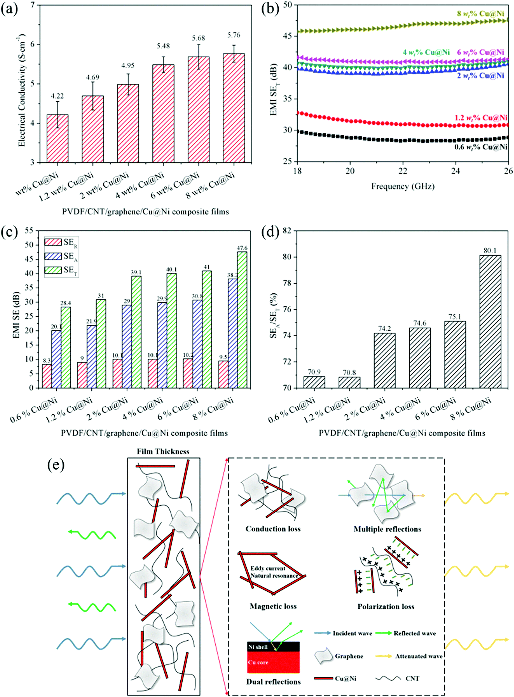
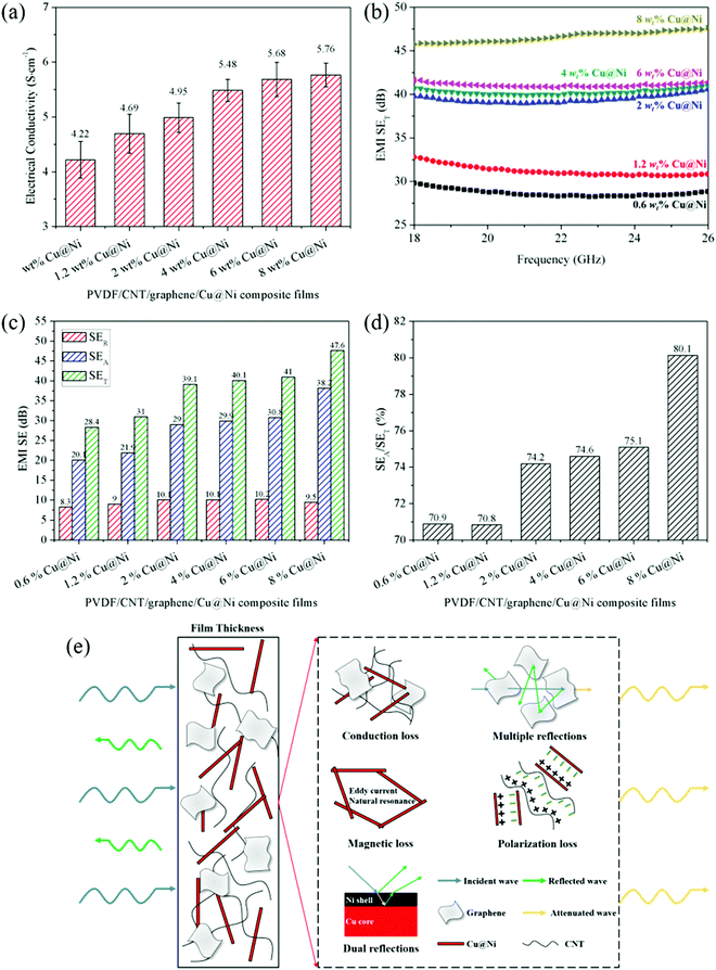
Fig. 5(a) shows the EC of the PVDF/CNT/graphene/Cu@Ni composite films with varying contents of the Cu@Ni nanorods. The EC increased from 4.6 S cm−1 to 5.8 S cm−1 as the Cu@Ni content increased from 0.6 wt% to 8 wt%. The FE-SEM images in Fig. 4 show that the increase in the Cu@Ni content shortens the distance between the graphene, CNTs, and Cu@Nis, thus promoting the bridging effect among the conductive fillers. The introduced CNTs and graphene scattered throughout the PVDF matrix, thus reducing insulated contacts. As a result, EC was retained in a high value of 4.22 S m−1 even at a low Cu@Ni content of 0.5 wt%. The motion of electrons was correspondingly accelerated through the formed conductive networks.51 This indicated that the increased EC was induced by a predominant contribution of denser and more developed electrically conductive pathways constructed by the fillers’ distribution in the PVDF matrix.
 |
| | Fig. 5 (a) EC of the PVDF/CNT/graphene/Cu@Ni composite films; (b) EMI SE of the composite films at a frequency from 18 GHz to 26 GHz; (c) the SE (SER, SEA and SET) and (d) the ratios of SEA/SET for the composite films at a frequency of 22 GHz; and (e) schematic EMI shielding mechanisms for the composite film. | |
Fig. 5(b) and Fig. S2 in the ESI† demonstrate that the EMI SE of the composite films continuously increased with the Cu@Ni content, which signified that EC and EMI SE had a close relevance.52,53 This relevance was ascribed to the attenuation of the EM waves using electrically conductive materials or materials which have electric and/or magnetic dipoles.54 On the one hand, the electron transfer that occurred on the surface of these materials gave rise to the reflection of the EM waves. Thus, higher EC caused more significant impedance mismatch at the interface between the free space and the materials’ surface to the benefit of the reflection loss.35 However, free electrons rarely existed on the surface of the CPCs, and thus the reflection loss from the CPCs’ surface was limited.55 On the other hand, when passing the metallic or conductive nanofillers, the incident EM waves were absorbed by the electric and/or magnetic dipoles interacting with the EM fields in the radiation.1 The absorbed EM wave energy was converted into heat via the Joule heating effect and was dissipated in the form of heat. Therefore, the increased EC simultaneously enhanced the reflection and absorption losses.
3.2.2 Mechanism of the EMI shielding performance.
The dominated EMI shielding mechanism of the Cu@Ni-decorated composite films in this study requires further explanation. As shown in Fig. 5(c), the values of SEA higher than SER are displayed based on the EMI SE results at 22 GHz. The values of SET, SEA, and SER for the Cu@Ni-decorated composite films with 6 wt% Cu@Ni are 41.0 dB, 30.8 dB, and 10.2 dB, respectively, of which SEA accounts for 75.1% of SET, for example. These larger proportions of SEA in SET than those of SER demonstrate that the composite films were absorption-dominated EMI shielding materials. Additionally, the values of SET and SEA increased dramatically with Cu@Ni contents, whereas those of SER levelled off at a high Cu@Ni content. Besides, the ratios of SEA/SET as shown in Fig. 5(d), which increased from 70.9% to 80.1%, further identified the attenuation of the Cu@Ni-decorated composite films as being mainly driven by the absorption loss. The absorption loss contributed by the Cu@Ni nanorods originated from the dielectric–magnetic (or core–shell) microstructure, impedance mismatch, intense interfacial polarization, eddy current loss and multiple reflections.39 Firstly, the EMI waves were absorbed through the complementary effects between magnetic loss and dielectric loss. The ferromagnetic Ni shell has a large aspect ratio and outstanding ability in magnetic loss and the Cu core possesses a strong dielectric loss performance. Additionally, the core–shell microstructure induced interfacial dipoles which existed among multiple interfaces between Ni/Cu, Ni/CNT and Ni/graphene systems in favor of the absorption loss.38 Lastly, the 1-D structured Cu@Ni nanorods formed a dissipation microcurrent and acted as an antenna receiver to absorb the incident EM wave energy,56 and the impedance match induced the EM wave to enter the interior of the receiver as much as possible. In summary, the introduced Cu@Ni nanorods dominated the attenuation of the EM wave by the absorption loss rather than the surface reflection loss.
Based on the above analysis, schematics of the synergetic effects of Cu@Ni nanorods and CNT/graphene on the EMI shielding performance are illustrated in Fig. 5(e). Firstly, the 1-D structure of CNTs and Cu@Ni nanorods was favorable to dissipate the microwave energy and induced an interfacial polarization loss.57 In particular, the polarization loss benefited from the increase in the charge accumulation of the aggregate dipoles at the interfaces between the fillers and the PVDF when the EM waves passed through the film.23 The migrating charges existing at the interface of Ni and Cu particularly induced interfacial polarization.58 Secondly, the introduced CNTs, graphene and Cu@Ni nanorods improved the EC according to the contacting and hopping conductive mechanism,27 thus enhancing the conduction loss associated with the attenuation of energy through the current flow. Thirdly, the conducting networks constructed by CNTs, graphene and Cu@Ni nanorods produced multiple reflection losses.59 Fourthly, dual reflection losses resulted from the interfaces in the core–shell microstructure of Cu@Ni nanorods.37 The EM waves were reflected at the Ni shell and then the waves transmitted from the Ni shell were reflected at the Ni/Cu interface. Finally, the dielectric loss, depending on the interfacial and dipole polarizations, and magnetic loss that originated from the eddy current and the natural resonance further attenuated the EM wave.60
3.2.3 Comparison of the EMI SE values of the composite films.
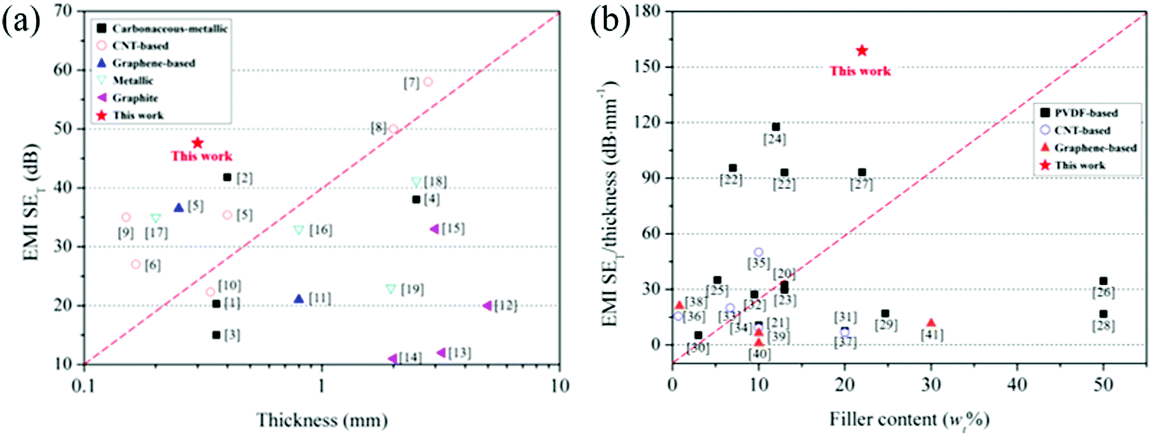
In general, the dominated absorption loss is directly in proportion to the thickness of the shielding material,1 but the thickening will increase the material consumption and hence the cost. It is, therefore, preferable to achieve high EMI SE values with relatively thin materials. To evaluate the EMI shielding performance of the prepared composite film, Table S2 in the ESI† and Fig. 6(a) show the EMI SE of some representative CPCs with thicknesses lower than 10 mm. The results show that, compared with other shielding CPCs, the SET of the composite film with 8 wt% Cu@Nis is located the farthest from the red line in the upper area of the comparison chart, indicating both the high EMI SE and thinness. To further evaluate the effectiveness of the shielding material by incorporating the EMI SE and the thickness (t), a more realistic parameter, SE/t, was applied.61 In addition to the EMI SE, thickness, filler type and content, it can be seen from Table S2 (ESI†) that the type of polymer matrix had a significant influence on the EMI performance. Therefore, the EMI SE/t values of the representative PVDF-based, CNT-based and graphene-based composites are shown for comparison in Table S3 of the ESI† and Fig. 6(b).
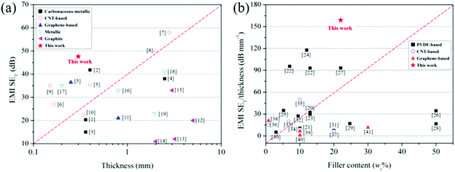 |
| | Fig. 6 Comparison of (a) EMI SE and (b) EMI SE/t of PVDF/CNT/graphene/Cu@Ni composite films with those in the literature. The numbers inside the panel are the reference numbers listed in Tables S2 and S3 in the ESI,† respectively. | |
Fig. 6(b) shows that the EMI SE/t of the composite film with 8 wt% Cu@Nis is the farthest from the red line in the upper area. Compared with the binary- or ternary-phase CPCs containing CNT,2,27 graphene27 and Ni chains29,62 in our previous studies as well as the PVDF-based, CNT-based and graphene-based CPCs shown in Fig. 6(b), this quaternary composite film exhibited the highest EMI SE/t value. As a consequence, the synergetic effects between Cu@Ni and CNT/graphene resulted in a stronger EMI shielding performance with thinness and low filler content than the single effect of CNT or graphene in the binary CPCs. The reinforcement in the EMI shielding performance contributed by CNT/graphene was mainly due to the high EC that was caused by the contacting and hopping conductive mechanisms from the hybrid of CNT/graphene. Thus, the conduction loss increased in alternating EM fields.27 Furthermore, CNT/graphene has a large aspect ratio, and thus its interfacial location provides abundant interfaces to multiply the reflections and attenuate the incident EM waves.63 With the introduction of Cu@Ni, the conduction loss was further enhanced because the CNTs and Cu@Ni nanorods filled the gaps between the graphene layers and bridged the neighboring fillers to form a conductive network.16 Moreover, the stacked morphology and agglomeration of CNT/graphene dramatically affected the electrical and EMI shielding properties of CPCs,30 whereas the high aspect ratio of the 1-D structure of Cu@Ni nanorods could prevent the agglomeration of CNT/graphene (see Fig. 4)6,26 and require a relatively low filler content as a conductive carrier56 to complete the conductive network. In one word, this composite film that was decorated by ternary conductive CNTs, graphene and 1D core–shell Cu@Ni nanofillers possessing collaborative advantages due to the conduction loss, interfacial polarization resulting from numerous interfaces, and dielectric–magnetic loss originating from the core–shell structured Cu@Ni, exhibited a stronger EMI shielding performance compared with our previous studies.
3.3 Thermal properties of PVDF/CNT/graphene/Cu@Ni composite films
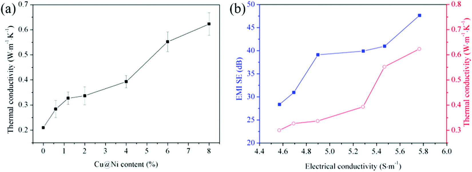
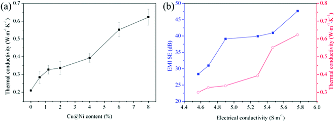
Prolonged exposure to EMI radiation caused the EMI shielding materials to be overheated, and therefore, a high TC is preferable to accelerate the heat dissipation of these materials.32 The TC of the PVDF/CNT/graphene/Cu@Ni composite films at room temperature is shown in Fig. 7(a). The TC of the Cu@Ni-decorated composite films continuously increased to 0.623 W m−1 K−1 at a Cu@Ni content of 8 wt%, which nearly tripled that of the pure PVDF with a value of 0.18–0.21 W m−1 K−1.29,64 As shown in Table 1, the TC of this composite film was comparable with that of some PVDF-based shielding CPCs in the literature. The augment in TC was attributed to the developed interconnectivity among the fillers and the matrix. The elevated TC facilitated the dissipation of heat that was converted from EM wave energy through the Joule heating effect.24
 |
| | Fig. 7 (a) TC of pure PVDF and PVDF/CNT/graphene/Cu@Ni composite films with various Cu@Ni contents and (b) correlation analysis of TC, EMI SE and EC. | |
Table 1 TC of the PVDF/CNT/graphene/Cu@Ni composite film and some representative PVDF-based composites in the literature
| Filler content |
TC (W m−1 K−1) |
Ref. |
| 1 wt% CNT/10 wt %Ni |
0.65 |
29
|
| 5 wt% GnP/8 wt %Ni |
0.66 |
29
|
| 8 wt% CNT/5 wt% Fe3O4 |
0.62 |
65
|
| 8 wt% graphene/5 wt% Fe3O4 |
0.68 |
65
|
| 16 wt% surface modified graphene |
0.679 |
66
|
| 6 wt% CNT/8 wt% graphene/8 wt% Cu@Ni |
0.623 |
This work |
The correlation analysis between the EMI SE and TC with respect to the EC is shown in Fig. 7(b). The results show that the incident EMI waves were attenuated with the increase in both EC and TC. The increase in the EC caused more EM wave energy conversion into Joule heat, and thus the high TC of the composite films was favorable to attenuate the incident EM waves through dissipating the converted heat.67,68 Accordingly, the collaborative improvement in the EC, TC and EMI SE with the increased content of Cu@Ni nanorods promoted the attenuation of the incident EM waves and prolonged the lifetime of the composite films.
3.4 Mechanical properties of PVDF/CNT/graphene/Cu@Ni composite films
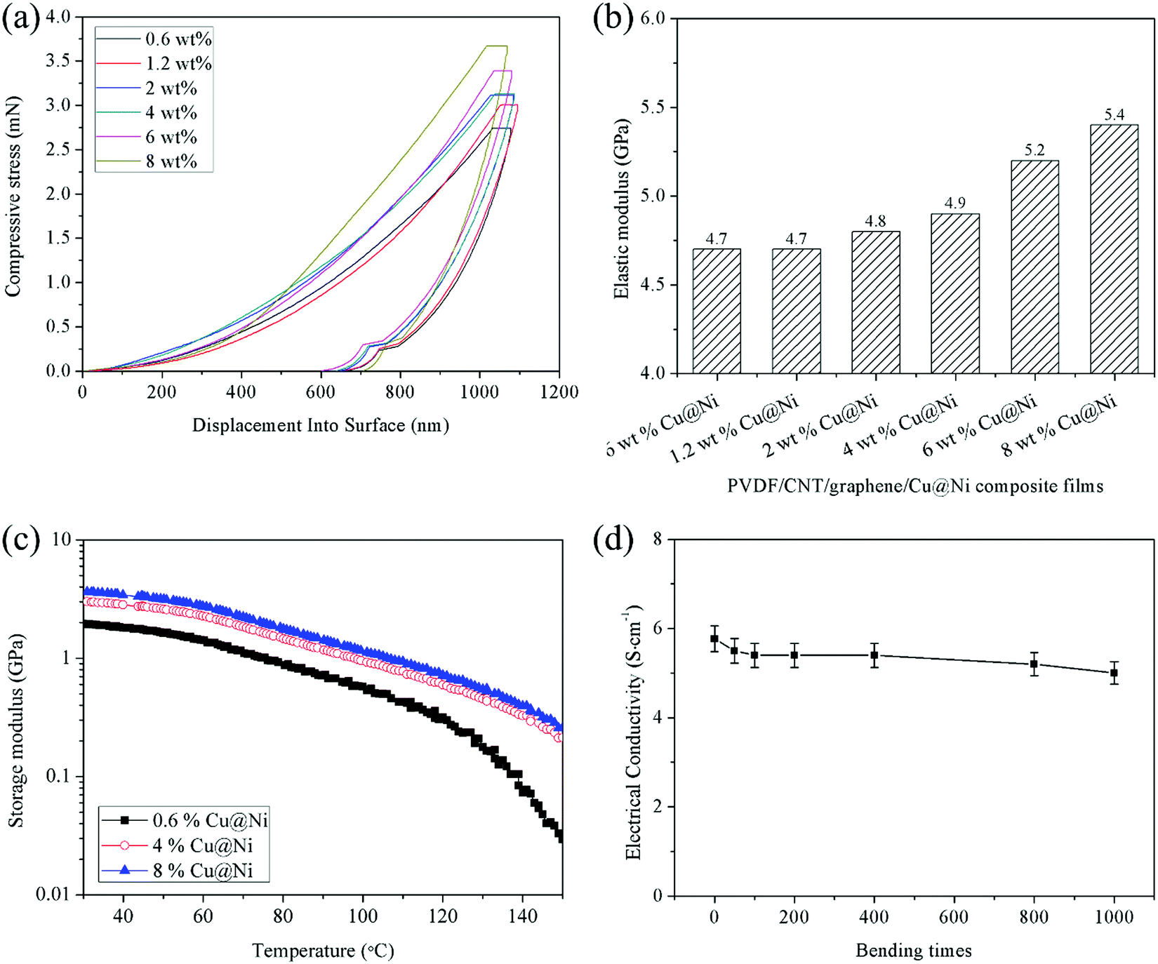
Based on the compression–displacement curve shown in Fig. 8(a), the elastic modulus of the composite film increased with the introduced Cu@Ni nanorods. The increased elastic modulus signifies a difficulty in the in-through elastic deformation of the Cu@Ni-decorated composite films. Therefore, greater stress is required to cause a certain in-through elastic deformation of the film (or conversely, a smaller in-through elastic deformation occurs under a given stress). The rigid section of the nanorods facilitated the extension, conformational transition, and movement of the polymer chain based on the pinning effect.18 Additionally, the distributed Cu@Ni nanorods increase the energy absorption and thus contribute to the elevated plastic deformation capacity. Fig. 8(c) shows that the storage modulus of the composite film with 0.6 wt% Cu@Ni decreases more sharply than that with a higher content of Cu@Ni nanorods, and the drop is obvious after the temperature exceeds 120 °C. This was attributed to the low TC of the composite film with 0.6% Cu@Ni, which indicated a tardy heat dissipation.
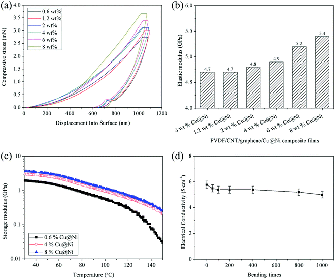 |
| | Fig. 8 (a) Compression versus displacement curve and (b) the elastic modulus of the composite films obtained using a nano-indenter; (c) storage modulus of the films as a function of temperature; (d) EC with 8 wt% Cu@Nis after repeated bending. | |
In addition to the high mechanical strength, the PVDF/CNT/graphene/Cu@Ni composite films exhibited an outstanding in-plane flexibility and structural integrity during bending. As shown in Fig. 1(c) and 8(d), the composite film with 8 wt% Cu@Ni could be repeatedly bent and exhibited a negligible decline in EC after repeated bending. This high electric stability of the composite film was attributed to the core–shell structure that prevents Cu from being oxidized, while the flexibility mainly originated from the carbonaceous fillers.1 The high flexibility and mechanical strength of the composite films make them suitable for various applications in flexible devices.
4. Conclusion
Flexible and robust PVDF/CNT/graphene/Cu@Ni composite films were fabricated via solution casting and compression molding. The EC, EMI SE and TC of the Cu@Ni-decorated composite films were adjusted by varying the Cu@Ni content. A strong EMI shielding performance of 158.8 dB mm−1 was exhibited due to the synergetic effect between the Cu@Ni nanorods and the carbonaceous nanofillers (CNTs and graphene). The prepared bimetallic Cu@Ni nanorods exhibited complementary effects in magnetic loss and dielectric loss, thus enhancing the contribution of absorption to the EMI shielding. Additionally, the EMI shielding performance was dominated by the absorption loss. Moreover, the developed interconnectivity of fillers with the increase in the Cu@Ni content not only accelerated the electrical and thermal conduction of the composite films to dissipate the converted heat, but also improved their flexibility and electric stability.
Conflicts of interest
There are no conflicts to declare.
References
- S. Sankaran, K. Deshmukh, M. B. Ahamed and S. K. K. Pasha, Composites, Part A, 2018, 114, 49–71 CrossRef CAS.
- B. Zhou,
et al.
, J. Mater. Chem. C, 2018, 6(31), 8360–8371 RSC.
- Z. Zeng, H. Jin, M. Chen, W. Li, L. Zhou and Z. Zhang, Adv. Funct. Mater., 2016, 26(2), 303–310 CrossRef CAS.
- J. Jang,
et al.
, Polymer, 2020, 186, 122030 CrossRef CAS.
- Y. J. Wan, P. L. Zhu, S. H. Yu, R. Sun, C. P. Wong and W. H. Liao, Small, 2018, 14(27), e1800534 CrossRef PubMed.
- C. Liang, M. Hamidinejad, L. Ma, Z. Wang and C. B. Park, Carbon, 2020, 156, 58–66 CrossRef CAS.
- B. Zhou,
et al.
, ACS Appl. Mater. Interfaces, 2020, 12(36), 40859–40869 CrossRef PubMed.
- Y. Q. H. Wei, J. D. Y. Du, X. Fang, W. Zheng, Y. Sun and Z. Jiang, Ceram. Int., 2017, 43(14), 10757–10762 CrossRef.
- B. Zhao,
et al.
, J. Mater. Chem. C, 2018, 6(38), 10292–10300 RSC.
- S. Zhang, S. Yin, Q. Ran, Q. Fu and Y. Gu, Polymer, 2019, 162, 20–28 CrossRef CAS.
- M. Han,
et al.
, ACS Appl. Mater. Interfaces, 2016, 8(32), 21011–21019 CrossRef CAS PubMed.
- K. Rajavel,
et al.
, Composites, Part A, 2020, 129, 105693 CrossRef CAS.
- F. Wu, A. Xie, M. Sun, W. Jiang and K. Zhang, Mater. Lett., 2017, 193, 30–33 CrossRef CAS.
- L. Liu,
et al.
, ACS Appl. Mater. Interfaces, 2018, 10(16), 14108–14115 CrossRef CAS PubMed.
- R. C. Che, L. M. Peng, X. F. Duan, Q. Chen and X. L. Liang, Adv. Mater., 2004, 16(5), 401–405 CrossRef CAS.
- E. Zhou,
et al.
, Carbon, 2018, 133, 316–322 CrossRef CAS.
- Q. Liu,
et al.
, Nanoscale, 2015, 7(5), 1736–1743 RSC.
- H. Zhang,
et al.
, Chem. Eng. J., 2020, 379, 122304 CrossRef.
- L. Liang,
et al.
, ACS Appl. Mater. Interfaces, 2019, 12(2), 2644–2654 CrossRef PubMed.
- L. Liang,
et al.
, Chem. Eng. J., 2020, 395, 125209 CrossRef CAS.
- M. Yu,
et al.
, J. Mater. Chem. C, 2014, 2(35), 7275–7283 RSC.
- J. Xu,
et al.
, Nanoscale, 2014, 6(11), 5782–5790 RSC.
- J. Zheng,
et al.
, Ind. Eng. Chem. Res., 2020, 59(8), 3425–3437 CrossRef CAS.
- X. Li,
et al.
, ACS Appl. Mater. Interfaces, 2018, 10(47), 40789–40799 CrossRef CAS PubMed.
- N. Wu,
et al.
, J. Mater. Chem. C, 2019, 7(6), 1659–1669 RSC.
- D. Jiang,
et al.
, Polym. Rev., 2019, 59(2), 280–337 CrossRef CAS.
- B. Zhao, C. Zhao, R. Li, S. M. Hamidinejad and C. B. Park, ACS Appl. Mater. Interfaces, 2017, 9(24), 20873–20884 CrossRef CAS PubMed.
- B. Zhao,
et al.
, J. Mater. Chem., 2019, 7(1), 133–140 RSC.
- B. Zhao,
et al.
, Carbon, 2018, 127, 469–478 CrossRef CAS.
- H. Abbasi, M. Antunes and J. I. Velasco, Prog. Mater. Sci., 2019, 103, 319–373 CrossRef CAS.
- H. K. Choudhary, R. Kumar, S. P. Pawar, U. Sundararaj and B. Sahoo, Carbon, 2020, 164, 357–368 CrossRef CAS.
- F. Ren,
et al.
, J. Mater. Chem. C, 2018, 6(6), 1476–1486 RSC.
- A. V. Menon, G. Madras and S. Bose, ChemistrySelect, 2017, 2(26), 7831–7844 CrossRef CAS.
- B. Zhao,
et al.
, Small, 2020, 202003502 Search PubMed.
- J. Li,
et al.
, Composites, Part B, 2020, 190, 107935 CrossRef CAS.
- P. Sambyal,
et al.
, Compos. Sci. Technol., 2019, 172, 66–73 CrossRef CAS.
- S. Wu,
et al.
, Small, 2018, 14(23), 1800634 CrossRef PubMed.
- B. Zhao, W. Zhao, G. Shao, B. Fan and R. Zhang, ACS Appl. Mater. Interfaces, 2015, 7(23), 12951–12960 CrossRef CAS PubMed.
- B. Zhao,
et al.
, CrystEngComm, 2017, 19(44), 6579–6587 RSC.
- N. Zhang,
et al.
, J. Alloys Compd., 2019, 784, 244–255 CrossRef CAS.
- Z. Jia,
et al.
, Composites, Part B, 2020, 183, 107690 CrossRef CAS.
- H. Zhao, M. Yang, D. He and J. Bai, J. Mater. Chem. C, 2016, 4(38), 8911–8919 RSC.
- M. Biswas, A. Saha, M. Dule and T. K. Mandal, J. Phys. Chem. C, 2014, 118(38), 22156–22165 CrossRef CAS.
- D. Y. Lee, M. Lee, K. J. Kim, S. Heo, B. Kim and S. Lee, Surf. Coat. Technol., 2005, 200(5–6), 1920–1925 CAS.
- P. Nie, C. Min, H. Song, X. Chen, Z. Zhang and K. Zhao, Tribol. Lett., 2015, 58(1), 7 CrossRef.
- H. Wang,
et al.
, Composites, Part A, 2016, 90, 606–613 CrossRef CAS.
- X. Ma, B. Shen, L. Zhang, Y. Liu, W. Zhai and W. Zheng, Compos. Sci. Technol., 2018, 158, 86–93 CrossRef CAS.
- S. Zhang and H. C. Zeng, Chem. Mater., 2010, 22(4), 1282–1284 CrossRef CAS.
- T. Yamauchi,
et al.
, Nanoscale, 2010, 2(4), 515 RSC.
- X. J. Zha,
et al.
, Composites, Part A, 2018, 105, 118–125 CrossRef CAS.
- H. Wang,
et al.
, Compos. Sci. Technol., 2016, 125, 22–29 CrossRef CAS.
- B. Zhao, G. Shao, B. Fan, W. Zhao, Y. Xie and R. Zhang, J. Mater. Chem. A, 2015, 3(19), 10345–10352 RSC.
- M. Cao, W. Song, Z. Hou, B. Wen and J. Yuan, Carbon, 2010, 48(3), 788–796 CrossRef CAS.
- F. Shahzad,
et al.
, Science, 2016, 353(6304), 1137–1140 CrossRef CAS.
- S. P. Pawar, S. Kumar, S. Jain, M. Gandi, K. Chatterjee and S. Bose, Nanotechnology, 2016, 28(2), 025201 CrossRef PubMed.
- B. Zhao,
et al.
, Eng. Sci., 2018, 3, 5–40 Search PubMed.
- J. Yang,
et al.
, ACS Appl. Mater. Interfaces, 2013, 5(15), 7146–7151 CrossRef CAS PubMed.
- S. He, C. Lu, G. Wang, J. Wang, H. Guo and L. Guo, ChemPlusChem, 2014, 79(4), 569–576 CrossRef CAS PubMed.
- Q. Liu,
et al.
, Adv. Mater., 2016, 28(3), 486–490 CrossRef CAS PubMed.
- Z. Shi,
et al.
, Adv. Mater., 2012, 24(17), 2349–2352 CrossRef CAS.
- A. Ameli, M. Nofar, S. Wang and C. B. Park, ACS Appl. Mater. Interfaces, 2014, 6(14), 11091–11100 CrossRef CAS PubMed.
- B. Zhao and C. B. Park, J. Mater. Chem. C, 2017, 5(28), 6954–6961 RSC.
- X. Hong and D. D. L. Chung, Carbon, 2017, 111, 529–537 CrossRef CAS.
- S. Biswas, I. Arief, S. S. Panja and S. Bose, ACS Appl. Mater. Interfaces, 2017, 9(3), 3030–3039 CrossRef CAS PubMed.
- H. Cheng,
et al.
, Composites, Part A, 2019, 121, 139–148 CrossRef CAS.
- B. Lin,
et al.
, Compos. Sci. Technol., 2019, 172, 58–65 CrossRef CAS.
- P. Zhang,
et al.
, Composites, Part A, 2019, 117, 56–64 CrossRef CAS.
- Y. Guo,
et al.
, Composites, Part A, 2019, 124, 105484 CrossRef CAS.
Footnote |
| † Electronic supplementary information (ESI) available. See DOI: 10.1039/d0ma00751j |
|
| This journal is © The Royal Society of Chemistry 2021 |
Click here to see how this site uses Cookies. View our privacy policy here. 
 Open Access Article
 This Open Access Article is licensed under a Creative Commons Attribution-Non Commercial 3.0 Unported Licence
 c,
Biao
Zhao
c,
Biao
Zhao