
 Open Access Article
 This Open Access Article is licensed under a
 Creative Commons Attribution 3.0 Unported Licence
Trends in additively manufactured microfluidics, microreactors and catalytic materials
Andrea
Rogolino
 *ab and
Gianpaolo
Savio
c
*ab and
Gianpaolo
Savio
c
aGalilean School of Higher Education, University of Padova, Italy. E-mail: andrea.rogolino@studenti.unipd.it
bDepartment of Chemical Sciences, University of Padova, Italy
cLaboratory of Design Tools and Methods in Industrial Engineering, Department of Civil, Environmental and Architectural Engineering, University of Padova, Italy
First published on 23rd November 2020
Abstract
The interest in microfluidics, that is the manipulation of fluids with volumes in the range of μL or below, has increased exponentially in the past decades, due to their relevance to diagnostics, sensors, drug-design and pilot plant prototyping. Common manufacturing processes in clean rooms for microfluidic substrates are well established, but still expensive and competence-demanding. Additive manufacturing is a promising alternative, given the inherent simple geometry and the small dimensions of microfluidic devices, which in turn allow ease of design and production along with a reduction of time and costs of the manufacturing processes. In this paper the state of the art in additive manufacturing of microfluidics and microreactors is presented, showing how vat photopolymerization, multimaterial jetting and extrusion-based additive manufacturing possess the best features in this field. An overview of the most remarkable applications obtained so far is provided, highlighting the best performance in layer height resolution achieved and the printing of dynamic devices. Furthermore, potentiality of additive manufacturing in the fabrication of catalysts for chemical reactions is reviewed. Finally, it is claimed how the rise of additive technologies in small-scale manufacturing in the future will definitely occur due to their cheapness, accessibility and ease of customization.
 Andrea Rogolino | Andrea Rogolino received his BSc in Chemistry at the University of Padova in 2020. He is currently enrolled as a student in the MSc Chemistry program at the University of Padova and in the class of Natural Sciences at the Galilean School of Higher Education of Padova. He was a visiting student at Donostia International Physics Center in San Sebastián, Spain in 2019 for an internship program. He was twice awarded at the International Chemistry Olympiads (Honourable Mention, Tbilisi 2016; Silver Medal, Nakhon Pathom 2017). His current research interests include artificial photosynthesis, catalysis and microfluidics. |
 Gianpaolo Savio | Gianpaolo Savio is an associate Professor at the Department of Civil, Environmental and Architectural Engineering at University of Padova. He graduated in Mechanical Engineering in 2004 at the University of Padova and in 2008 he obtained the PhD in Design and Methods for Industrial Engineering at the University of Bologna. Gianpaolo is active in the research community as an author, a reviewer and a member of the editorial board for several international journals and conferences. The main research topics concern CAD tools and Design for Additive Manufacturing. Since 2007 he has taught “Engineering drafting” and “Geometric modeling of mechanical systems” at the University of Padua. |
Introduction
Microfluidics is a very recent research field consisting of the study and setup of technologies to handle volumes of liquids between μL and nL regimes. The possibilities introduced by this modern field are relevant to different areas, including physics, materials science, optics, microelectronics, chemistry, biology, medicine, bioengineering and microengineering. The birth of the microfluidic chip has often been compared to that of integrated circuits in electronics and people are making efforts to merge these two technologies. Microfluidic systems are classified as MEMS, Micro Electro Mechanical Systems, which are extremely relevant to sensors and diagnostic devices. These devices bring important benefits among which are: (i) considerable saving of time both in synthetic and analytical processes, (ii) reduction of feed and waste, (iii) cost reduction, (iv) easy control of inlet and outlet flux granted by low Reynolds number, and (v) efficient thermal and chemical diffusion. Diagnostics is by far one of the most interesting fields of application. Household and portable blood sugar testers are just examples of how microfluidics has become part of our daily life. Today, clinics can perform a great number of preliminary tests in a few seconds with a single drop of blood. Microfluidics opens up interesting perspectives; among the most promising fields are pharmaceutical industries and plant reactors (for instance, for the miniaturisation of pilot plants). Combinatorial chemistry is a further area of interest whose development highly depends on microfluidics. Combinatorial chemistry aims at running tens of chemical reactions simultaneously by mixing small quantities of reagents in different combinations, so as to detect and choose the most desirable product in high yield.1 Furthermore, lab-on-a-chip (or LoC – as they are often referred to – that is, a system capable of reproducing a functional chemical or biological laboratory at the scale of centimeters or below, as shown in Fig. 1)2 might contribute to the growth of Green Chemistry that is the development of environmentally and energetically responsible procedures of synthesis, use and waste of chemicals. Indeed, chips would allow limited use of solvents, energy saving and waste reduction.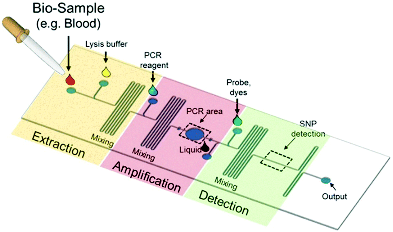 | ||
| Fig. 1 Scheme of a lab-on-a-chip. Adapted from 2. | ||
To highlight the ever-growing interest for this new research area, in 2001 the Royal Society of Chemistry founded the journal Lab on a Chip, in which several articles from engineers, chemists and biologists are published every year.
Although most microfluidic chips are traditionally fabricated through photolithography or soft lithography, additive manufacturing (AM) is a promising alternative. AM technologies allow one to print complex geometries and easy-to-customize pieces on the basis of thermodynamics and fluid dynamics. In addition, they are suitable to make lattice structures and millimetric reaction tanks. Although an improvement in resolution is still required, 3D printing provides cheapness and wide accessibility to users with no special expertise, since both hardware and software tools are easy to learn and manage.
In this paper, state of the art and perspectives of AM in microfluidics are discussed. First, a comparison between traditional manufacturing process and additive technologies is provided. Then, remarkable applications in the production of microfluidic circuits, microreactors and catalysts are presented.
Traditional methods of production of microfluidic systems
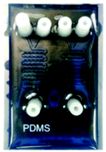
The two main techniques currently spread for the manufacturing of micro/nano-circuits are photolithography3–5 and soft lithography.6–8 Both techniques provide resolution up to few nms and work on elastomeric resins, in particular polydimethylsiloxane (PDMS).9 PDMS is the predominant polymer for the production of lab-on-a-chip devices due to its properties: resistance to temperature, chemical attack and oxidation; excellent electrical insulation; resistance to aging; transparency; biocompatibility; chemical inertia; no toxicity or flammability.10Among the soft lithographic techniques – so called because of the use of easy to mould elastomeric resins - is micro-molding.11 Through this technique, moulds carved with the reliefs of the flow channels are fabricated; afterwards the resin is heated and injected or compressed into the mould.
Photolithography, on the other hand, consists in creating mould patterns with the help of photosensitive compounds (photoresists) and then overlapping the mould with the elastomer, which in turn gets the proper shape. Photoresist and opaque masks are arranged so as to shape the positive or negative frame of the mould. A light source is then applied changing a property of the photoresist, such as its solubility in a given solvent.12 Excess or supporting photosensitive materials can be removed by leveraging on this property. Finally, the elastomeric resin (PDMS) is moulded into the photoresist template. Later on, the elastomer can be bonded to glass or other surfaces.
The peculiarity of both these techniques is the need for expensive, bulky, sensitive and clean equipment. As a result, qualified personnel and a dust-protected working environment, i.e. a clean room, are essential.13
Among other traditional techniques, laser cutting is worth a mention. By this production method, microfluidic channels are shaped with a laser beam (typically a CO2-laser).14–17 Its main advantages are simpler equipment, which does not strictly require a clean environment and a lower number of production steps. This technique has already been used to fabricate biocompatible and PMMA-based labs-on-a-chip.14,15,18 Although cheaper than soft lithography,18,19 laser cutting provides much lower resolution (tens of micrometers versus hundreds of nanometers) and often spoils the material by excessive burning. For this reason, carbon residues need to be accurately removed with solvents.16,17 Laser cutting might be still applied to low-resolution microfluidics, including for educational and demonstrative purposes.
Additive technologies in microfluidics: an overview
According to the Scopus database,20 searching by “Additive Manufacturing” AND “Microfluidics” in Title, Abstracts and Keyword, only 227 papers are found, and most studies appeared only in the last 7 years. The application of 3D printing in the production of microfluidic components is attractive for several reasons. First, it reduces the large number of steps required by soft lithography, since the production is obtained by direct addition of materials, bypassing the need for moulds or masks for each layer.21–33 The limited printing volume of the current machines is not an issue: on the contrary, it can be further reduced so as to install a manufacturing tool simply on a desk with no loss of production quality.34 Materials are a further advantage, since most microfluidic devices are made of polymers that can be directly processed via AM and are often biocompatible or derived from biotechnologies.32,35–37 Glass microfluidic devices were also additively manufactured.29,38–41 The geometry complexity is easy to set in a STL file, while in photolithography and soft lithography, it highly depends on the number of subsequent refinements. While support material for applications of AM technologies is critical, that is not the case in microfluidics, since it is often removed by thermal or mechanical extraction through the channels “dug” during printing. Although it has lower resolution, AM allows much lower production times. Indeed, the promoters of AM in microfluidics embrace a “fail fast and often” strategy: although several tests may be needed, the complete production of a simple fluid mixer takes up to less than 15 minutes.42Labs-on-a-chip and similar circuits are suitably “printed” by three AM technologies:43 vat photopolymerization, material jetting and material extrusion.44
Vat photopolymerization
Photopolymerization is currently the predominant technique in microfluidics. The technique is sometimes called “vat” because it is actually composed of a bath of liquid, polymerizable resin. This in turn is point by point illuminated by a UV light beam, which initiates hardening of the material by photopolymerization. The design to be manufactured is shaped by accurately directing the light. Vat photopolymerization is divided into two main variants, stereolithography (SLA) and digital light processing (DLP). In SLA, a laser beam is directed to the surface of a liquid resin bath moving in the xy plane to selectively polymerize the resin. After a layer is completed, the built plate is then moved downwards or upwards. In DLP, the resin is polymerised by means of a digital mirror device (DMD), i.e. a reflective plane formed by millions of micrometric mirrors, which reproduce, pixel by pixel, the image of the layer to be printed. The laser is then reflected by the DMD towards the photosensitive resin through a converging lens. This provides the advantage of printing the entire layer at the same time, avoiding the need for an xy pointer. Printing times are reduced accordingly.42The most distinguishing quality of these methodologies is certainly resolution, the highest of all AM. Photopolymerization is the only technology currently capable of creating structures well below 100 μm wide, comparable with classical techniques. In 2017, Nordin et al. from Brigham Young University achieved the goal of a surface area of 18 μm × 20 μm for a fluid transport channel using a custom printer.45 Materials particularly suitable for microreactors, like silica dispersions, have been prepared and processed with stereolithography.46 Microreactors printed by photopolymerization have been used in kinetic studies and synthesis in organic chemistry.47,48 Here, the transparency of the resin was a great advantage, which allowed the use of optical sources for photocatalysis or characterization. The potential of vat photopolymerization for the production of sub-100 μm devices has been predicted and simulated with mathematical models.49,50 The technique allows static and dynamic elements to be printed. There are well-known examples of circuits comprising valves and peristaltic pumps.51,52 Similar possibilities are also feasible by inkjet printing.44
Photopolymerization is promising in terms of costs, dropping up to $100 for a machine.42 More devices in parallel are used in laboratories where this technology has been introduced. Finally, post-processing operations are often straightforward because the excess liquid resin can be evaporated or drained. However, a severe limitation of stereolithography is the restriction to monomaterial applications.
Material jetting
Material jetting is the second most relevant AM methodology for microfluidics. The principles of material jetting are basically the same of a common 2D printer. A printhead is free to move on a plane dropping liquid inks, which subsequently solidify after thermal (cooling) or photo-induced (UV curing) treatment. Multiple inks can be cast on a single layer, such as one for the product and one for supports. These are removed afterwards by post-processing. The possibility to adopt different materials for one single manufacturing opens up new scenarios. In particular, multi-material printers (multi-jet modeling, MJM) have been used in microfluidics for the fabrication of circuits, allowing high structural complexity, thanks to the possibility to add layers of different materials for product and support structures. Removal of the latter is based on differences in the properties of materials (solubility, thermal stability, etc.). The multi-material implementation allows, as for photopolymerization, the creation of static, dynamic, rigid and flexible components. This is why MJM is often relevant to the printing of pumps and valves. Material jetting can work in a continuous or batch process. The latter case is the preferred method for microfluidic printing, since it produces smaller droplets as long as the “ink” of the material has an adequate viscosity. A further classification of material jetting technology includes distinction between powder-bed deposition and photopolymer deposition. The latter can mix up to 14 different materials in a single print.42The best results achieved with this method so far include geometries between 100 and 60 μm wide. In addition, studies suggest that the grooves in micro-channels are more stable when printed vertically.42,53–55
Although it is an attractive option, multi-material jetting always requires demanding post-processing. Packed supports are often impossible to remove directly. Secondary materials are often removed by thermal methods (e.g. melting of some waxes used as supports), immersion in solvents (different solubility of the materials allows selective removal) or sonication (ultrasound attack destroys target materials). Material jetting technology is still the most expensive, with costs between 10 and 100 times higher than those required by vat photopolymerization or material extrusion. The study of materials – which must meet clear criteria of transparency, density and biocompatibility – represents a crucial factor in the development of MJM in microfluidics, especially looking for applications in biomedical devices.
One of the first applications of material jetting in microfluidics was provided by the pioneering work by Whitesides et al., where 3D printing was first used for the fabrication of sub-millimetric molds for PDMS devices.56 Subsequently, molds for PDMS57 as well as proper microfluidic devices were made with an acrylic-based resin.58 A thorough analysis of the limits of resolution achievable with inkjet technology by the prototyping of microreactors was also reported.59 As a further strategy, material jetting was also used to print joinable modules.60 Moreover, applications for biomedical purposes and diagnostics have been proposed.61,62
Material extrusion
This is by far the most popular AM technology, as well as the one acknowledged by most as actual “3D printing”. The proper name for this methodology is fused deposition modelling (FDM) and it consists of the fabrication of three-dimensional pieces by subsequent deposition of layers of a polymeric material (most commonly ABS and PLA). The material is unwound from a spool and conveyed to a movable heated extruder. Here, the polymeric filament is fused and ejected through a nozzle on the underlying layer. Material extrusion is easy to use, comfortable, safe, quite reliable over time and generally cheap. Post-processing is considerably simplified, which makes it an excellent solution to reduce waste material. Although these characteristics should encourage its application, FDM has severe limitations in accuracy. Being based on the extrusion of a polymeric material that is deposited in adjacent rows, it is extremely difficult to adapt it to the manufacturing of pieces, whose dimensions fall below one millimetre. Printing times are also much longer than those required by vat photopolymerization or material jetting, as the layers are built point by point. The real potential of material extrusion comes from a surprising peculiarity of this technology: the process can be easily interrupted and launched again at any time. Scotti et al. took advantage of this feature to allow the insertion of a magnetic stirrer into the reaction vessel of a 3D printed polypropylene reactor before closing the structure by subsequent extrusion.63FDM for chemistry and microfluidics was pioneered by Cronin and coworkers, who reported the low-cost fabrication of a reactor comprising scaffolds for electrochemical and spectroscopic analyses. The authors also reported applications for both organic and inorganic syntheses.64 Microreactors comprising few mm width channels have been printed using polypropylene as a printing material.65,66
A brief comparison of the technologies described so far is in Table 1.
| Technology | Advantages | Limitations | Minimum channel thicknessa | Main ref. |
|---|---|---|---|---|
| a The minimum width achieved in microfluidic coils. Printer model is reported in brackets. | ||||
| Vat photopolymerization | Highest resolution | Mainly toxic polymers | 18 μm (BYU custom 3D printer)67 | 42, 44, 48, 50, 67 and 68 |
| Easy customization by varying curing depth, wavelength, intensity and time. | Long times | |||
| Easier removal of non-polymerized material (post-processing) | Monomaterial | |||
| Material jetting | Multimaterial | Expensive | ∼60 μm (Projet 3000HD+)59 | 42 and 59–62 |
| Suited to print movable structures (e.g. valves) | Difficult post-processing | |||
| Printing of multiple devices at a time | Not many biocompatible materials | |||
| Material extrusion | Very easy to use | Very low resolution | ∼500 μm (Felix 3.0)69 | 42, 65, 66, 69 and 70 |
| Short times | Long times | |||
| Very cheap | Mainly applicable for batch millimetric reactors | |||
| Easy post-processing | ||||
| Possibility to stop and restart the printing process at any time | ||||
Applications
Templates for PDMS
The simplest application of 3D printing in microfluidics is the production of templates for PDMS. The added value of 3D printing is the ability to achieve complex designs in a single step, such as multi-layer templates or pipes of variable thickness. In addition, 3D printing allows considerable saving of time and equipment.Digital light processing photopolymerization has already been extensively run-in, leading to excellent results. In particular, the DLP printer produced by Miicraft® (Taiwan, China) – whose high performance in printing accuracy has earned it a prominent place in both orthodontics and jewellery industries - has a resolution between 30 and 60 μm in the xy spacing, while up to 5 μm in layer height.
In a method developed by Comina et al.,71 DLP technology was used to produce PDMS templates with a transversal resolution of 56 μm and a vertical resolution of 50 μm. Their Miicraft® printer worked on an acrylate resin not compatible with PDMS. This required a tailored post-processing. The authors treated printed templates with ultrasound before applying a coating with a suitable ink (Pentel NN60). The PDMS was then poured onto the base and heated to 65 °C for 2 hours. The method was applied to produce templates that included guides for the insertion of vertical tubes aimed at the introduction and mixing of liquids (Fig. 2). This allowed a much easier installation process. Although the initial purchase cost for a machine is around $2500, production costs dropped to $0.48 cents per template (Miicraft®). In addition, it has been verified that thicknesses of the printed pipes do not affect the economy of the project. The same method was also used in the production of templates for multilayer microfluidics. Templates proved to be reusable several times without loss of quality or important damage.71
 | ||
| Fig. 2 PDMS templates with silica tubing guides. Adapted with permission from 71. | ||
Valves by a customized 3D printer
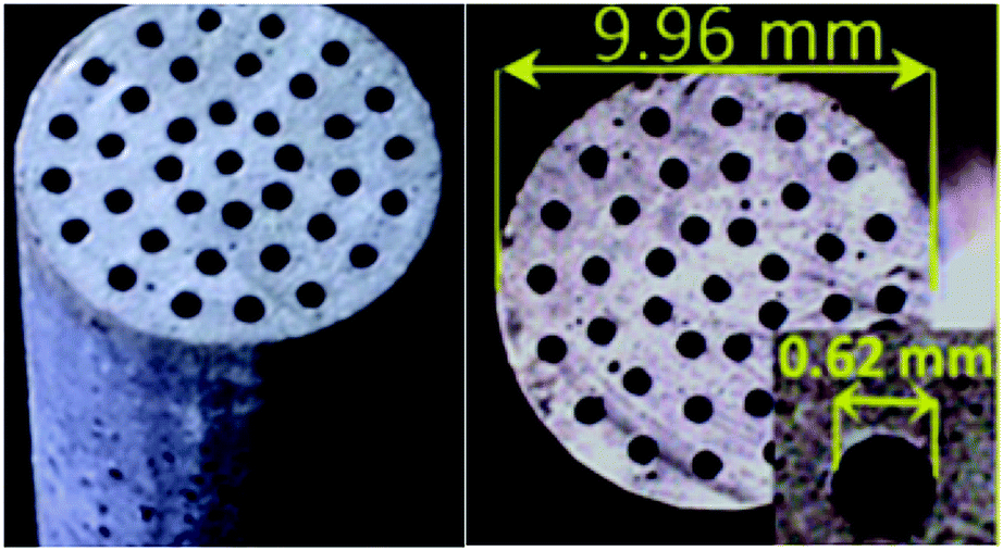
A significant contribution to the development of high-resolution DLP printing was made by Nordin et al.51,67,68,72,73 who built a DLP device and developed custom software on Python to operate it.Their printer features a volume of just a few mm3 (coils as big as 0.12 mm3 have been printed) and a UV LED (395 nm wavelength) for light curing, which allows a wider choice of UV-absorbent material than the more common LEDs (usually 405 nm wavelength). The printing material contains a polyethylene glycol diacrylate (PEGDA) resin, an organic photoinitiator and a component for UV light absorption. The latter was selected from a list of suitable substances by means of a systematic protocol where materials that did not meet certain requirements were stepwise rejected. In particular, the following properties have been evaluated: solubility in PEGDA resin, photo-absorbing capacity, optical penetration in the resin, required exposure time and influence on mechanical resistance. This research shows how much work is still needed to optimize small-scale additive technologies and that innovation will mainly come from the discovery of new materials and methods on existing machinery rather than from the invention of new printing techniques.
Nordin et al. also developed a mathematical model to predict the minimum layer height that can be achieved with their printer depending on the exposure time to UV light, the absorbance of the polymer and the concentration of the photoabsorbent species, ending with a value of 18 μm. Actually, they were able to produce channels with a section of 18 μm × 20 μm, which is the best performance achieved so far by additive technologies.67
Also, they applied their research to the manufacturing of microvalves, meeting ever improving results in the past few years (Fig. 3).51,67,68,72,73 Their custom 3D printer allowed us to print valves with a diameter as small as 150 μm (Fig. 4).
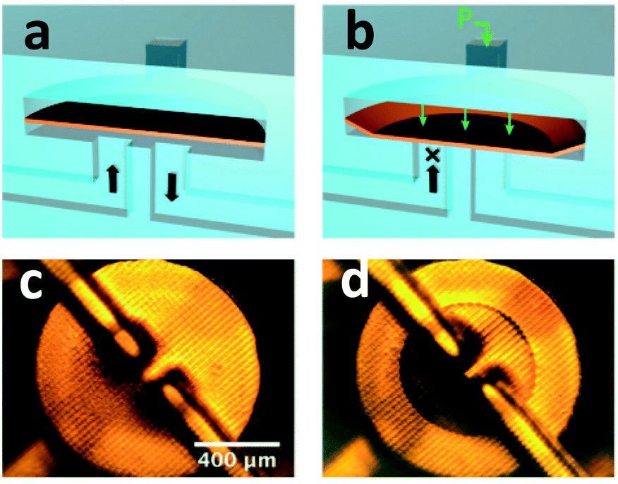 | ||
| Fig. 3 Microvalves fabricated with a DLP-SLA 3D printer by Nordin et al. (a and b) schematic pictures of an open (a) and closed (b) valve; (c and d) microscope pictures of an open (c) and closed (d) valve. Adapted with permission from 51. | ||
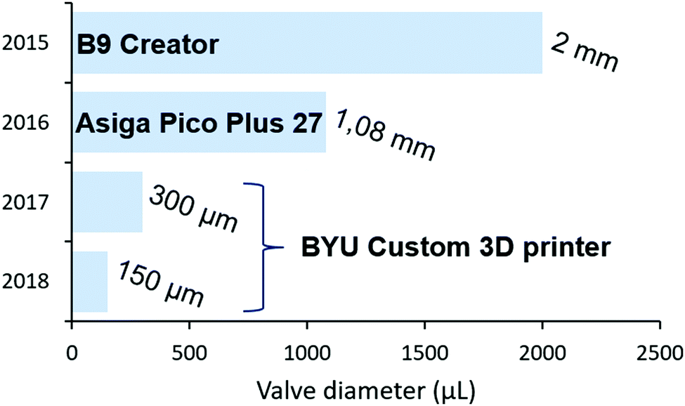 | ||
| Fig. 4 Progressive minimum valve diameters achieved by additive manufacturing technologies. Models of printers are reported in bold on the graph. | ||
Integrated microfluidic circuits
In industrial plants, as well as in laboratories, mechanical devices able to convey, pump and interrupt flows are fundamental. In recent years, this led to the development of integrated microfluidic circuits (ICFs). ICFs (based on classic integrated circuits from electronics) are miniaturized plants comprising pipes, valves, pumps and switches to convey liquids. In 2015, a team of researchers in mechanical and biomedical engineering produced and tested ICF components using multi-material jetting.74 Results have shown that the technology is particularly suitable because it allows the user to choose different materials according to the required mechanical properties at each point.In addition, as with photopolymerization, resolution lowers to tens of μm. The study shows how to successfully manufacture “capacitors” (channels with variable section), “diodes” (non-return valves) and “transistors” (valves with switch function). Names and pictures associated with each of these devices strongly recall the world of electronics. Condensers were designed as circular vessels between two pipes with a diaphragm capable of expanding and retracting according to the pressure exerted by the current fluid. Diodes had a similar structure but with an internal diaphragm that encloses two circular vessels. Transistors behaved as diodes with a more complex design (Fig. 5). The method followed to produce these components highlights the potential of microfluidic material jetting printing. Two nozzles, ejecting photosensitive monomer for the product and wax for the support structures, were used. The printed object was adhered on an aluminium surface, then kept in an ice bath for about five minutes to facilitate the detachment of the piece. To remove the support structures, these were heated to 80 °C in an oven and an oil bath to liquefy the wax in the outer layers. Complete removal of wax was accomplished by injecting hot oil directly into the printed pipes and then drying with compressed air. This resulted in a design with a minimum layer height of 32 μm and printing times of 4–5 hours for the most sensitive components such as transistors. Finally, experiments were carried out at room temperature to test the correct operation of the circuits. This work has shown that material jetting technology enables the production of versatile, flexible components with the most complex geometries, featuring good resolution and reasonable printing times.74
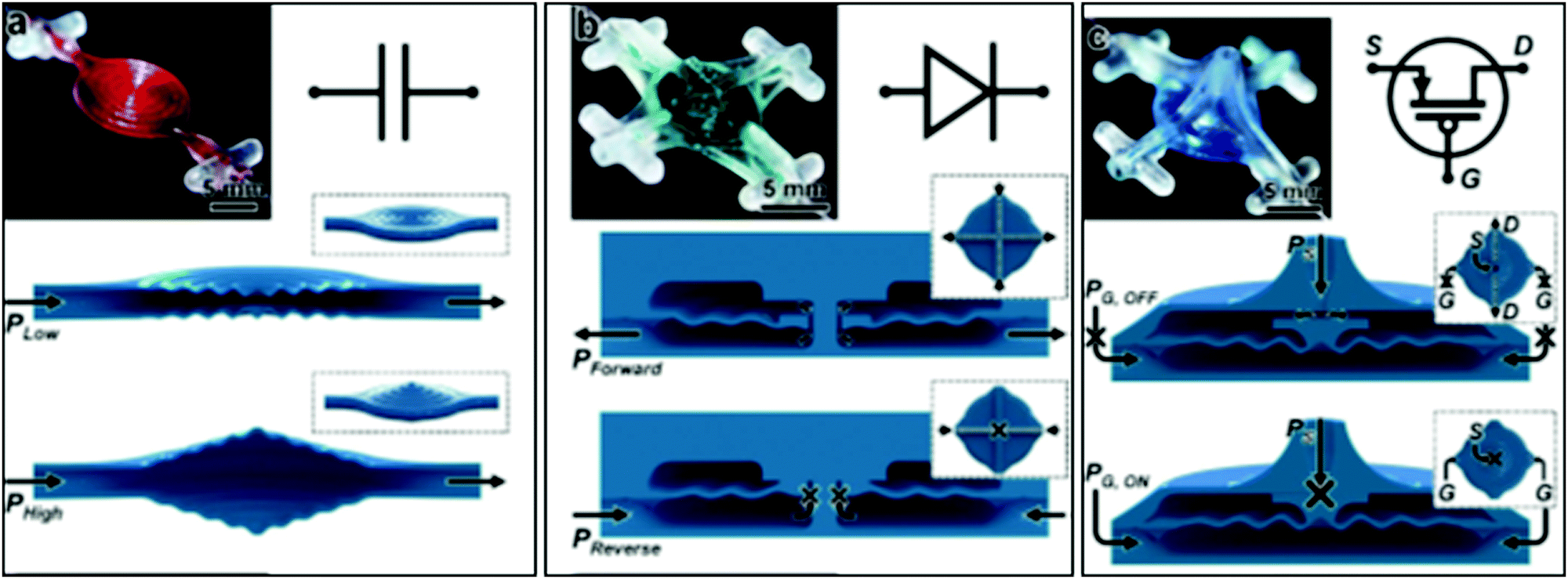 | ||
| Fig. 5 Microfluidics electronics similitude: (a) capacitor: diaphragm expands with high incoming pressure, (b) diode: fluid can flow from upper to lower vessel, but the opposite path is prevented by a tapping diaphragm, and (c) transistor: with the aid of an auxiliary fluid pressure is exerted on a piston, which in turn closes the inlet into the upper vessel. Adapted with permission from 74. | ||
Catalysts
An important and relatively recent field of application of AM is the modelling of heterogeneous catalysts to be used in industry as well as microreactors. Catalysts are materials capable of increasing the rate of chemical reactions. Catalytic power is mostly determined by surface to volume ratio: larger contact area corresponds to higher catalytic efficiency. 3D printing might give an asset to fulfil this requirement. Porous catalysts often require long synthetic processes under well-controlled conditions. Additive technologies, on the other hand, make it possible to create structures on which solid particles can precipitate, or adhere, according to the desired geometry. Multi-material printing represents a further strength. Hybrid catalysts, which include both organic and inorganic units, are of utmost importance in chemistry. Through direct inkjet deposition it is possible to formulate the desired composition a priori and “draw” the most suitable profile.For a start, polymers themselves can be extruded to build grids with catalytic activity. Nonetheless, due to their small surface area, it is necessary to mix them with inorganic species such as metal oxides. Difficulties arise in the preparation of the composite material, which should maintain its physico-chemical properties throughout the printing process.
This approach has also been adapted to vat photopolymerization, although it is more convenient to produce templates on which to model the catalytic material. This strategy was investigated by Michorczyc et al., whose work was to design and print a hollow cylinder containing cylindrical bars to be used as a mould for a multi-cavity catalyst (Fig. 6).75
 | ||
| Fig. 6 The metal/metal oxide hollow catalyst from the work by Michorczyc et al. Adapted with permission from 75. | ||
Finally, vat photopolymerization allows the polymerization of properly functionalized monomers. Functional groups, that are small branching groups of atoms, are exposed to the surface of the polymer and work as reaction centres (Fig. 7). Digital light processing allows good control on shape and surface exposure.76
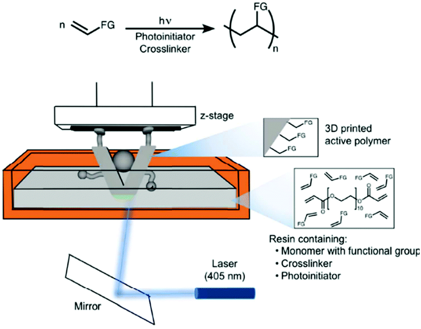 | ||
| Fig. 7 Schematic example of polymerization in SLA with surface catalytic functional groups (FGs). Adapted with permission from 76. | ||
Carbonisation of extruded thermosetting polymers can yield carbon-based catalysts. The resorcinol–formaldehyde resin, having a high degree of cross-linking, maintains its structure after being carbonized at 900 °C. It also has good rheological properties that make it suitable for extrusion. Zhou and Liu from Tianjin University in China, printed a palladium-coated carbon structure, which showed good catalytic activity in methane combustion (Fig. 8).77 This demonstrates how remarkable results can be achieved even with limited resources such as an extrusion-based 3D printer and an oven.
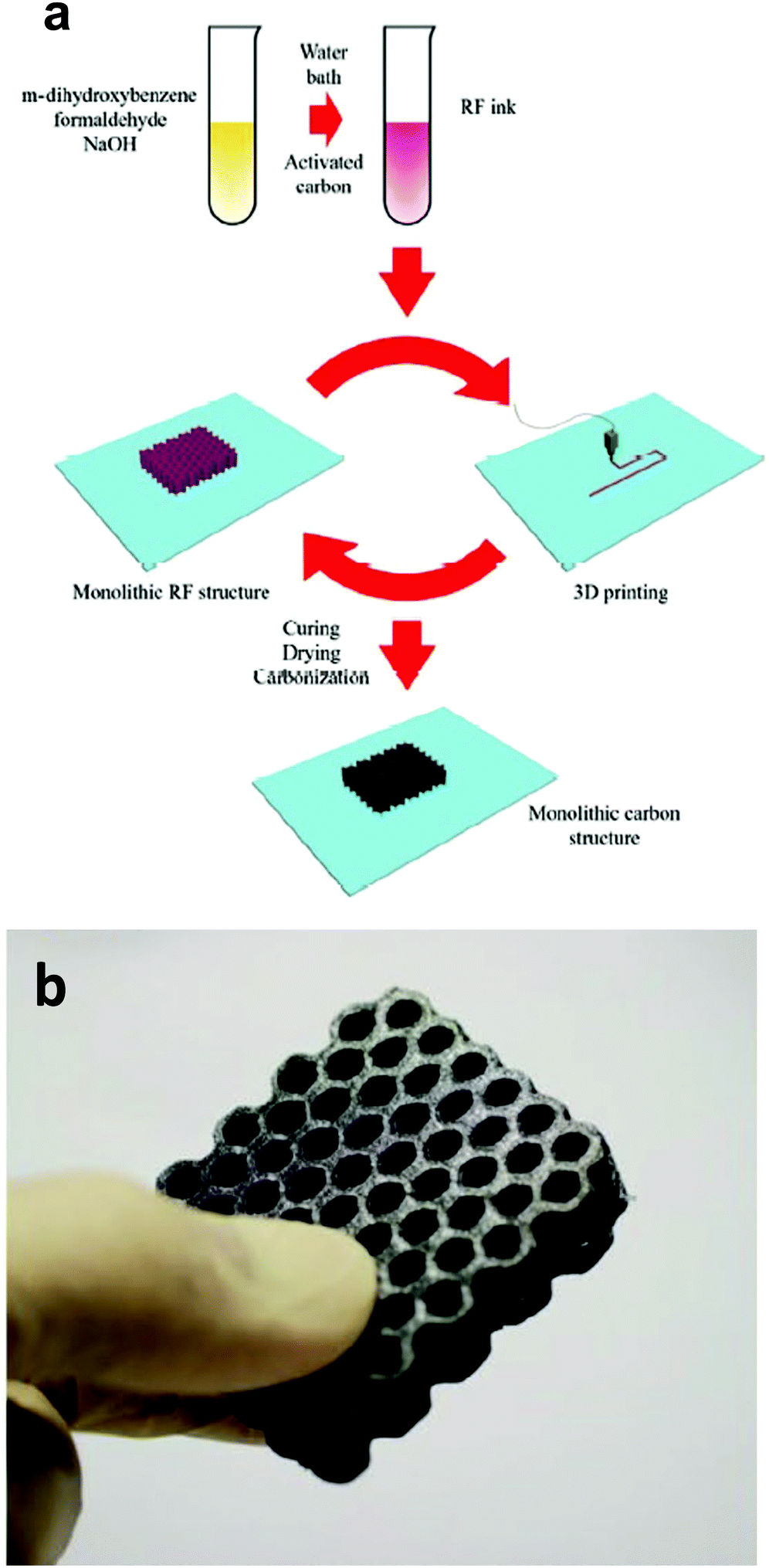 | ||
| Fig. 8 (a) Production of a porous catalyst via deposition of an RF cross-linked resin, and (b) printed catalyst after carbonization in an oven. Adapted with permission from 77. | ||
Most of the techniques described so far comprise the deposition of a metallic material on the printed substrate, which in turn determines the catalytic activity. This post treatment can be avoided by preparing inorganic powders modified so as to work in material jetting technology. Tubìo et al. managed to extrude a powder of aluminium and copper compounds, whose viscosity had been modulated with methylcellulose, into a three-dimensional lattice structure (Fig. 9).78 The monolith was then sintered at 1400 °C to allow the organic component to evaporate. This resulted in excellent catalytic properties in organic reactions along with a high degree of recyclability. After 10 reaction cycles the catalysts showed no signs of degradation. The method is particularly promising for ease and speed of production. A similar strategy has been applied to print zeolites, extremely porous materials often used to filter gas, among which is CO2.
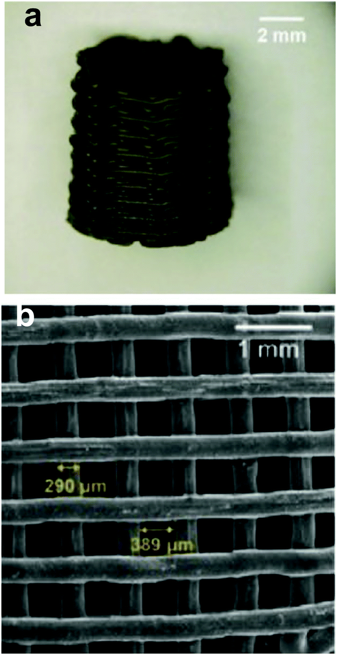 | ||
| Fig. 9 Lattice image (a) and SEM image (b) of a mesh structure of a catalytic material obtained through jetting of inorganic salts followed by sintering. Adapted with permission from 78. | ||
Highly porous metallic materials are also the typical products of selective laser melting (SLM), an AM technology exclusively concerned with metals or semiconductors. Metallic cells can be designed and properly carved by a high-energy laser beam conveyed on a powder bed. SLM allows the manufacturing of multi-pore structures with a tunable porosity gradient.79 Although the application of this technique to pristine catalytic metals (Pd, Pt, Ag, and Au) has yet to be improved, applications with alloys in flow chemistry have been reported. 316 L stainless steel is a very common substrate for SLM and it has been used in the production of small catalytic vessels.55,80 Still, the resolution of this technique is well below that of traditional micromachinery, having the minimum achievable wall thickness of around 0.5 mm.55 Thus, its application is limited to millimetric catalytic materials or supports. Further limitations arise from the difficulty of removing excess powder through the narrow pores of the product. To date, there are not many available materials for SLS and some alloys might suffer from dealloying due to the local temperature increase caused by the laser.81 Nonetheless, very recent applications in chemistry have been reported. Stainless steel with parametrized porosity manufactured by SLM was used as a support for a copper catalyst in hydrogen production by methanol steam reforming.79 Other applications for metallic catalysts showed good reusability.82 Other than metals, SLM has been used to prepare silicon-based materials relevant to different technologies.83
Future perspectives and conclusions
Labs-on-a-chip and microfluidics are still definitely recent technologies (born in the early ‘80s), while the application of additive manufacturing in the field has only been investigated since a few years ago. Intense efforts are still needed to extend the feasibility and accuracy of certain technologies to increasingly complex cases and systems of daily use. Even if photolitography and other traditional techniques will likely dominate for a long time, we wish to pinpoint three main advantages of AM in microfluidics: economy, customizability and wide accessibility.3D printing surely allows considerable cost saving by providing an alternative to the strict working conditions imposed by traditional techniques. The price of a printer for recreational use has now dropped to ∼ $200 for material extrusion. Production costs are significantly lower, as shown for Miicraft® in the study case of printed PDMS templates at $0.48 each.71
Structures difficult and expensive to achieve by photopolymerization can be easily realized by changing print settings or STL files. Channels of different thicknesses, multi-level templates and tubing guides51,67,71 are clear evidence of this customizability. Creating catalysts with large surface area and porous features is sometimes impossible with other techniques. Hardware can be customized as well, as demonstrated by Nordin and Gong.67
AM allows one even to rethink technical processes, so that its customizability is applicable to practical problem-solving. In a work by Rossi et al., a microfluidic circuit for organic synthesis was simplified by removing a cumbersome filtration step needed after the reaction. Thanks to a homemade FDM 3D printer, the researchers could fabricate an integrated setup including mixing coils and tubing guides for the filtration column (Fig. 10).84 This is a clear example of how researchers with no advanced knowledge of engineering or computer science can improve their work by means of ready-to-use additive technologies.
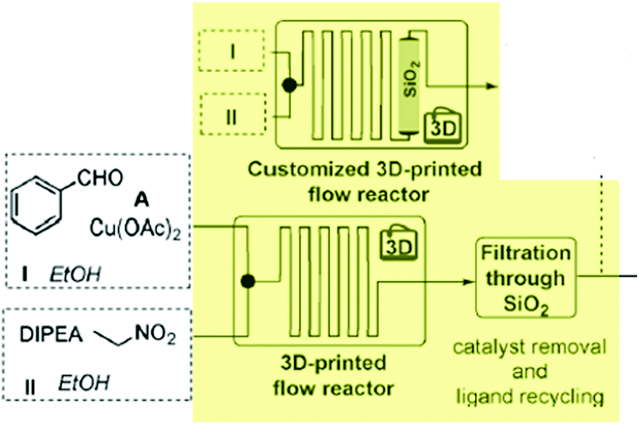 | ||
| Fig. 10 Workflow of the synthetic process by Rossi et al. Highlighted in yellow: inclusion of the filtration process in the customized 3D-printed flow reactor. Adapted with permission from 85. | ||
Future perspectives include a plethora of applications. Most recent ones include sensors for engineering and medicine,86 inertial microfluidic devices for cell and particle separation87 and organs-on-chips.88
However, the greatest benefit of additive technologies is to extend the art of manufacturing to an ever-widening audience. Little maintenance is required and machines need few settings to be started. Barrow et al. installed three Ultimaker® extrusion-based printers in their laboratory to make microfluidic circuits for research purposes on their own.89 AM also encourages communication since groups can easily share designs to be printed.90,91
An ever-wider library of software for design can be found nowadays. MineLoC, for instance, might represent a revolution in 3D modelling for microfluidics. It consists of a procedure to design labs-on-a-chip through the Mineways platform, an open source rendering program developed according to the logic of the popular videogame Minecraft (Fig. 11). Models created can be exported as STL files. It is possible to create designs with a volume of up to 1000 × 1000 × 120 voxels.92 Finally, as remarked by Walsh et al., makerspaces (fab labs) might be “the new clean rooms”, thus promoting so called DIY chemistry, biology and medicine.17
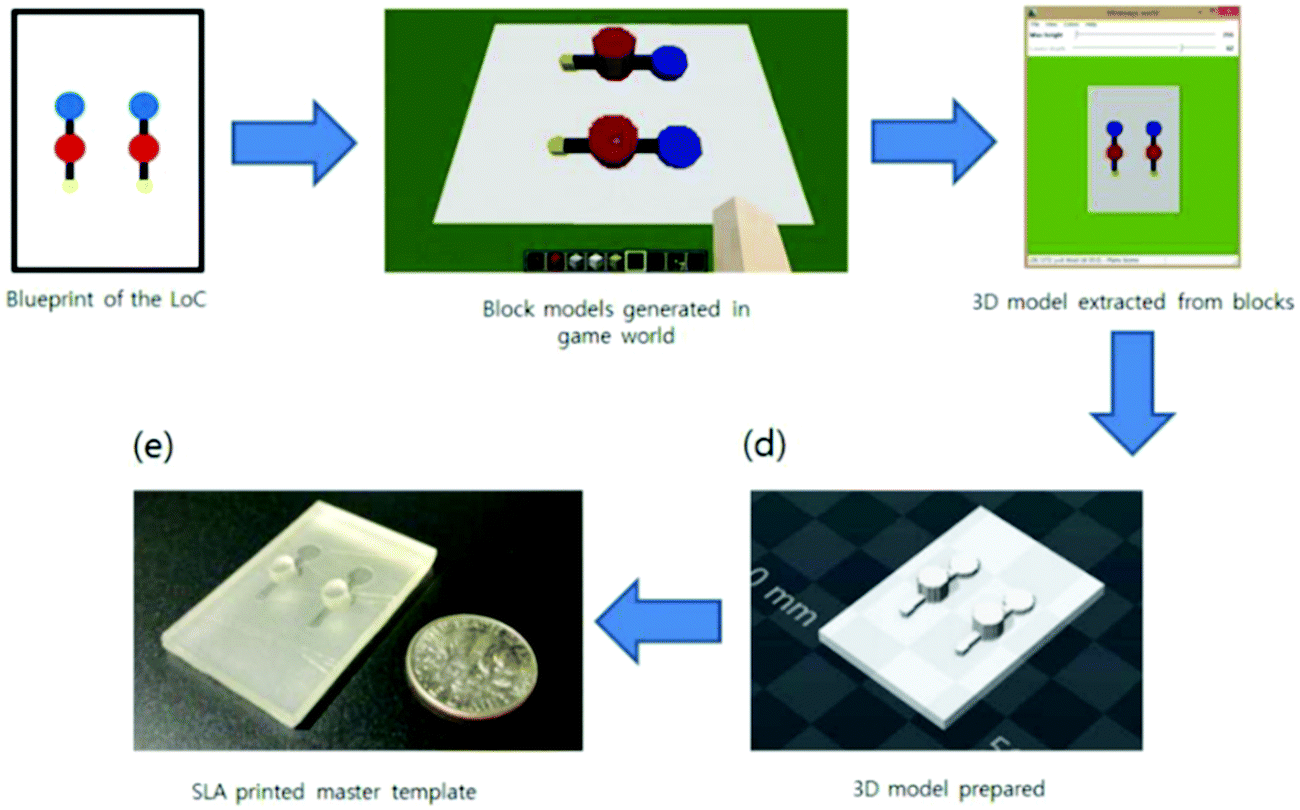 | ||
| Fig. 11 Pictures from Mineways modeling environment. Adapted from 92. | ||
More specifically, we believe that the expansion of additive manufacturing in microfluidics will start, as it is already occurring, with FDM technologies. In spite of their very poor resolution, more and more scientists are conceiving 3D printers as an essential lab tool. Deposition methods will be particularly suitable for the rapid prototyping of microreactors in order to study chemical reactions under controllable operational conditions.
Vat photopolymerization is likely to be the next technology to be included in every microfluidics lab. Polymeric materials are the most suitable for the production of miniaturized laboratories. Upcoming works from materials science will definitely provide us with a variety of resins, possibly biocompatible, having interesting elastic properties and durability. Moreover, fabricated chips are usually transparent, so that liquid flows are easier to observe and characterize via optical methods (e.g. spectroscopy). The future of labs-on-a-chip highly depends on the advances in this technology especially in resolution.
Material jetting will be the dominating additive technology for the manufacturing of mobile parts in labs-on-a-chip. Valves and switches are just two examples. Indeed, this is the only technique allowing easy combination of materials to achieve a one-shot fabrication of composite tools, combining rigid and soft moieties. So far, microfluidics has been concerned with vessels and pipes of fixed sizes, mostly because of the limitations of traditional methods. The works presented in this paper strongly suggest to us that multi-jet modelling (MJM) might trigger a revolution in microfluidics, leading to actual micro machinery for the manipulation of fluids, comprising blades, screws and pumps. This would be the rise of something which could be named mechano microfluidics.
In conclusion, the applications of additive manufacturing to micro-scale devices will grow in the following years if efforts are made on its peculiar features, rather than on mimicking methods already applied by traditional techniques. In any case, we wish to point out that, in the past decades, many research areas from natural sciences, engineering and industry have been shifting their interest towards small dimensions, as demonstrated by the uprising of nanoscience. In the future, technologies will have to cope with ever-smaller dimensions, while maintaining a high spatial resolution.
Conflicts of interest
There are no conflicts to declare.Notes and references
- G. A. Cooksey, C. G. Sip and A. Folch, Lab Chip, 2009, 9, 417–426 RSC.
- C.-W. Huang, et al. , Microarrays, 2015, 4, 570–595 CrossRef CAS.
- D. Allen, Galvanotechnik, 2009, 100, 1426–1430 CAS.
- D. Brambley, B. Martin and P. D. Prewett, Adv. Mater. Opt. Electron., 1994, 4, 55–74 CrossRef CAS.
- L. Geppert, IEEE Spectrum, 1996, 33, 33–38 Search PubMed.
- Y. Xia and G. M. Whitesides, Angew. Chem., Int. Ed., 1998, 37, 550–575 CrossRef CAS.
- Y. Xia and G. M. Whitesides, Annu. Rev. Mater. Sci., 1998, 28, 153–184 CrossRef CAS.
- J. A. Rogers and R. G. Nuzzo, Mater. Today, 2005, 8, 50–56 CrossRef CAS.
- J. C. McDonald, et al. , Electrophoresis, 2000, 21, 27–40 CrossRef CAS.
- L. Malaquin, et al. , Microelectron. Eng., 2002, 61–62, 379–384 CrossRef CAS.
- M. Heckele and W. K. Schomburg, J. Micromech. Microeng., 2004, 14 Search PubMed.
- J. T. M. Stevenson and A. M. Gundlach, J. Phys. E: Sci. Instrum., 1986, 19, 654–667 CrossRef CAS.
- S. Khumpuang and S. Hara, IEEE Trans. Semicond. Manuf., 2015, 28, 393–398 Search PubMed.
- H. Klank, J. P. Kutter and O. Geschke, Lab Chip, 2002, 2, 242–246 RSC.
- Y. Huang, et al. , Appl. Surf. Sci., 2010, 256, 1675–1678 CrossRef CAS.
- P. Nath, et al. , Lab Chip, 2010, 10, 2286–2291 RSC.
- D. I. Walsh, et al. , Trends Biotechnol., 2017, 35, 383–392 CrossRef CAS.
- D. Patko, et al. , Sens. Actuators, B, 2014, 196, 352–356 CrossRef CAS.
- R. Samuel, et al. , J. Micromech. Microeng., 2014, 24, 105007 CrossRef.
- Scopus, https://www.scopus.com/search/form.uri?display=basic&zone=header&origin= (accessed 26 October, 2020).
- A. K. Au, et al. , Angew. Chem., Int. Ed., 2016, 55, 3862–3881 CrossRef CAS.
- T. Naito, et al., presented in part at 18th International Conference on Miniaturized Systems for Chemistry and Life Sciences, MicroTAS 2014, San Antonio, Texas, USA, October 2014.
- C.-H. Chu, R. Liu, T. O. Ahmadov and A. F. Sarioglu, presented in part at 22nd International Conference on Miniaturized Systems for Chemistry and Life Sciences, MicroTAS 2018, Kaohsiung, Taiwan, November 2018.
- U. M. Sonmez, et al. , Micromachines, 2020, 11(4), 384 CrossRef.
- A. Mohammadzadeh, A. E. Fox-Robichaud and P. R. Selvaganapathy, J. Micromech. Microeng., 2019, 29, 015013, DOI:10.1088/1361-6439/aaf25a.
- F. Zhu, N. P. MacDonald, J. M. Cooper and D. Wlodkowic, Proc. SPIE, 2013, 8923, 892344, DOI:10.1117/12.2033400.
- W. Su, B. S. Cook and M. M. Tentzeris, IEEE Trans. Microwave Theory Tech., 2016, 64, 1928–1936 Search PubMed.
- P. G. Shankles, L. J. Millet, J. A. Aufrecht and S. T. Retterer, PLoS One, 2018, 13, e0192752, DOI:10.1371/journal.pone.0192752.
- F. Kotz, K. Plewa, C. Richter and B. E. Rapp, presented in part at 19th International Conference on Miniaturized Systems for Chemistry and Life Sciences, MicroTAS 2015, Gyeongju, Korea, October 2015.
- P. Juskova, et al. , Anal. Chim. Acta, 2018, 1000, 239–247 CrossRef CAS.
- J. Lölsberg, et al. , Lab Chip, 2018, 18, 1341–1348 RSC.
- M. J. Männel, L. Selzer, R. Bernhardt and J. Thiele, Adv. Mater. Technol., 2019, 4, 1800408, DOI:10.1002/admt.201800408.
- J. Kajtez, et al. , Adv. Sci., 2020, 7, 2001150, DOI:10.1002/advs.202001150.
- F. Zhu, N. P. MacDonald, J. M. Cooper and D. Wlodkowic, Proc. SPIE, 2013, 8923, 892344, DOI:10.1117/12.2033400.
- C. K. Dixit, K. Kadimisetty and J. Rusling, TrAC, Trends Anal. Chem., 2018, 106, 37–52 CrossRef CAS.
- F. B. Holness, T. L. Poepping and A. D. Price, Proc. SPIE, 2019, 10966, 1096606, DOI:10.1117/12.2514379.
- S. Zips, et al. , Adv. Mater. Technol., 2019, 4, 1800455, DOI:10.1002/admt.201800455.
- E. Gal-Or, et al. , Anal. Methods, 2019, 11, 1802–1810 RSC.
- F. Kotz, D. Helmer and B. E. Rapp, Proc. SPIE, 2018, 10491, 104910A, DOI:10.1117/12.2287654.
- H. Elsayed, et al. , Addit. Manuf., 2019, 28, 365–372 CAS.
- L. Jonušauskas, et al. , Proc. SPIE, 2018, 10520, 105201G, DOI:10.1117/12.2286906.
- S. Waheed, et al. , Lab Chip, 2016, 16, 1993–2013 RSC.
- ISO/ASTM 52900:2015 Additive manufacturing – General principles – Terminology, 1–9, DOI: 10.1520/ISOASTM52900-15.
- R. D. Sochol, et al. , Microelectron. Eng., 2018, 189, 52–68 CrossRef CAS.
- H. Gong, et al. , Lab Chip, 2017, 17, 2899–2909 RSC.
- M. Wozniak, et al. , J. Eur. Ceram. Soc., 2009, 29, 2259–2265 CrossRef CAS.
- S. Corbel, et al. , Virtual Phys. Prototyping, 2012, 7, 203–209 CrossRef.
- T. Monaghan, et al. , Lab Chip, 2016, 16, 3362–3373 RSC.
- M. J. Beauchamp, G. P. Nordin and A. T. Woolley, Anal. Bioanal. Chem., 2017, 409, 4311–4319 CrossRef CAS.
- H. Gong, et al. , RSC Adv., 2015, 5, 106621–106632 RSC.
- H. Gong, A. T. Woolley and G. P. Nordin, Lab Chip, 2016, 16, 2450–2458 RSC.
- A. K. Au, et al. , Lab Chip, 2015, 15, 1934–1941 RSC.
- F. Calignano, et al. , Proc. IEEE, 2017, 105(4), 593–612, DOI:10.1109/JPROC.2016.2625098.
- H. Bikas, P. Stavropoulos and G. Chryssolouris, Int. J. Adv. Des. Manuf. Technol., 2016, 83, 389–405 CrossRef.
- A. J. Capel, et al. , Lab Chip, 2013, 13, 4583–4590 RSC.
- J. C. McDonald, et al. , Anal. Chem., 2002, 74, 1537–1545 CrossRef CAS.
- Y. Hwang, O. H. Paydar and R. N. Candler, Sens. Actuators, A, 2015, 226, 137–142 CrossRef CAS.
- A. Bonyár, et al. , Procedia Eng., 2010, 5, 291–294 CrossRef.
- R. Walczak and K. Adamski, J. Micromech. Microeng., 2015, 25, 85013 CrossRef.
- K. G. Lee, et al. , RSC Adv., 2014, 4, 32876–32880 RSC.
- S. A. N. Gowers, et al. , Anal. Chem., 2015, 87, 7763–7770 CrossRef CAS.
- O. H. Paydar, et al. , Sens. Actuators, A, 2014, 205, 199–203 CrossRef CAS.
- G. Scotti, et al. , React. Chem. Eng., 2017, 2, 299–303 RSC.
- M. D. Symes, et al. , Nat. Chem., 2012, 4, 349–354 CrossRef CAS.
- P. J. Kitson, et al. , Lab Chip, 2012, 12, 3267–3271 RSC.
- J. S. Mathieson, et al. , Beilstein J. Nanotechnol., 2013, 4, 285–291 CrossRef.
- H. Gong, et al. , Lab Chip, 2017, 17, 2899–2909 RSC.
- H. Gong, A. T. Woolley and G. P. Nordin, Lab Chip, 2018, 18, 639–647 RSC.
- N. P. Macdonald, et al. , Anal. Chem., 2017, 89, 3858–3866 CrossRef CAS.
- J. M. Lee, M. Zhang and W. Y. Yeong, Microfluid. Nanofluid., 2016, 20, 5 CrossRef.
- G. Comina, A. Suska and D. Filippini, Lab Chip, 2014, 14, 424–430 RSC.
- C. I. Rogers, et al. , Biomicrofluidics, 2015, 9, 1–9 CrossRef.
- G. P. Nordin, H. Gong and A. T. Woolley, presented in part at Solid-State Sensors, Actuators and Microsystems Workshop, Hilton Head Island, South Carolina, USA, 2018.
- R. D. Sochol, et al. , Lab Chip, 2016, 16, 668–678 RSC.
- P. Michorczyk, E. Hȩdrzak and A. Wȩgrzyniak, J. Mater. Chem. A, 2016, 4, 18753–18756 RSC.
- J. S. Manzano, et al. , ACS Catal., 2017, 7, 7567–7577 CrossRef CAS.
- X. Zhou and C. J. Liu, Adv. Funct. Mater., 2017, 27, 1–13 Search PubMed.
- C. R. Tubío, et al. , J. Catal., 2016, 334, 110–115 CrossRef.
- J. Liu, et al. , Int. J. Hydrogen Energy, 2020, 45, 10–22 CrossRef CAS.
- C. Parra-Cabrera, et al. , Chem. Soc. Rev., 2018, 47, 209–230 RSC.
- J. J. Brandner, Fabrication of Microreactors Made from Metals and Ceramic, in Microreactors in Organic Chemistry and Catalysis, ed. T. Wirth, 2013, DOI:10.1002/9783527659722.ch2.
- S.-X. Liang, et al. , Appl. Mater. Today, 2020, 19, 100543, DOI:10.1016/j.apmt.2019.100543.
- T. Minasyan, et al. , Ceram. Int., 2018, 44, 13689–13694 CrossRef CAS.
- S. Rossi, et al. , J. Chem. Educ., 2015, 92, 1398–1401 CrossRef CAS.
- S. Rossi, et al. , Angew. Chem., Int. Ed., 2017, 56, 4290–4294 CrossRef CAS.
- M. R. Khosravani and T. Reinicke, Sens. Actuators, A, 2020, 305, 111916 CrossRef CAS.
- S. Razavi Bazaz, et al. , Sci. Rep., 2020, 10, 5929 CrossRef CAS.
- H. Sun, et al. , Curr. Opin. Chem. Eng., 2020, 28, 1–9 CrossRef.
- https://ultimaker.com/it/learn/cardiff-university-accessible-3d-printed-microfluidic-devices. (accessed 26 October 2020).
- A. J. L. Morgan, et al. , PLoS One, 2016, 11, 1–17 Search PubMed.
- J. Li, et al. , Adv. Sci., 2020, 7, 1901719 CrossRef CAS.
- K. Kim, et al. , Sensors, 2018, 18, 1896 CrossRef.
| This journal is © The Royal Society of Chemistry 2021 |