
 Open Access Article
 This Open Access Article is licensed under a Creative Commons Attribution-Non Commercial 3.0 Unported Licence
Light-activated gas sensing: a perspective of integration with micro-LEDs and plasmonic nanoparticles
Jun Min
Suh†
 *,
Tae Hoon
Eom†
,
Sung Hwan
Cho†
,
Taehoon
Kim
and
Ho Won
Jang
*
*,
Tae Hoon
Eom†
,
Sung Hwan
Cho†
,
Taehoon
Kim
and
Ho Won
Jang
*
Department of Materials Science and Engineering, Research Institute of Advanced Materials, Seoul National University, Seoul 08826, Republic of Korea. E-mail: hwjang@snu.ac.kr
First published on 9th December 2020
Abstract
Light-activated gas sensors have been investigated for their superior potential to replace current thermally activated gas sensors, which have several drawbacks for the Internet of Everything application. This review summarizes the various efforts made for the development of light-activated gas sensors and provides an overview of their progress. The light-activated gas sensing properties of metal oxides, 2D materials, and other candidate materials are summarized. As strategies to overcome the current challenges of light-activated gas sensors, the effects of nanostructures and crystallographic orientations are discussed. Finally, the incorporation of plasmonic nanoparticles and integration with micro light-emitting diodes are proposed for the pathway toward the real application of light-activated gas sensors. This review should offer a broad range of readers a new perspective toward the future development of light-activated gas sensors.
 Jun Min Suh | Jun Min Suh is Postdoctoral Associate at Research Institute of Advanced Materials, Department of Materials Science and Engineering, Seoul National University. He earned his PhD from the Department of Materials Science and Engineering, Seoul National University in August, 2020. His research focuses on nanostructured electronic materials including metal oxides and 2D materials for gas sensor applications. |
 Tae Hoon Eom | Tae Hoon Eom is a PhD candidate in the Department of Materials Science and Engineering in Seoul National University. His research focuses on the synthesis of 2D materials and their applications in light-activated room-temperature gas sensors. |
 Sung Hwan Cho | Sung Hwan Cho is a PhD candidate in the Department of Materials Science and Engineering in Seoul National University. His research focuses on room-temperature colorimetric gas sensors and metal oxide-based gas sensors. |
 Ho Won Jang | Ho Won Jang is an Associate Professor in the Department of Materials Science and Engineering in Seoul National University. He earned his PhD from the Department of Materials Science and Engineering in Pohang University of Science and Technology in 2004. He worked as a Research Associate at the University of Wisconsin-Madison from 2006 to 2009. Before he joined Seoul National University in 2012, he worked in Korea Institute of Science and Technology as a Senior Research Scientist. His research interests include the synthesis of oxides, 2D materials, and halide perovskites, and their applications in nanoelectronics, solar water splitting cells, chemical sensors, plasmonics, metal–insulator transition, and ferroelectricity. |
1. Introduction
With the emerging Internet of Everything (IoE) era, the significance of sensor technologies has been emphasized and led to a dramatic development in sensor technologies during the last decade.1 With the IoE platform, the inter-connections between various sensors and mobile devices can collect numerous helpful data from the surrounding environments and process them into useful information for modern human life. These various sensors can be classified into five groups depending on the five human senses: vision for the image sensor, touch for a pressure sensor, hearing for voice recognition, taste for an electronic tongue, and smell for gas sensors. The gas sensors in IoE applications are required to have a small size with low power consumption for their embedding in portable devices, not to mention excellent gas sensing performance.2To achieve the requirements for IoE application, various gas sensor principles have been suggested including cantilever-based gas sensors,3 capacitive gas sensors,4 thermometric gas sensors,5 optical gas sensors,6 field-effect transistor gas sensors,7 colorimetric gas sensors,8 solid-state electrochemical gas sensors,9,10 or chemoresistive gas sensors.11–13 Among them, the chemoresistive gas sensors have been considered the most appropriate due to their simple structure with easy fabrication processes and low cost. These advantages can result in small size and compatibility with the existing electrical circuits, suitable for the IoE application. Their working principles are based on the resistance change upon adsorption and desorption of target gas molecules on the surface of semiconductors.
The chemoresistive gas sensors usually utilize various semiconducting materials including metal oxides,14–22 2-dimensional (2D) materials,23–30 or conductive polymers.31–33 Although each material has been reported for its superior gas sensing characteristics to specific target gas molecules through various strategies, a common challenge exists, which is the high operating temperature. Metal oxides require operating temperatures around 250–350 °C for the activation of the interaction with gas molecules.34 Two-dimensional materials and conductive polymers are usually capable of operating at low temperatures near the room temperature, but some amount of heat should be provided to overcome their slow kinetics in the aspect of practical applications. Therefore, heaters have been irreplaceable components in gas sensors, but they induce thermal degradation of the nearby electronic components during operation, causing limitation in the miniaturization and low reliability of sensor systems, which is the primary reason for high-power consumption.35
As an alternative to heaters, the light source, in particular light-emitting diodes (LEDs), has been one of the great candidates for the activation of semiconductors or gas-sensing materials at low temperatures.36,37 The appropriate choice of light wavelength with a higher energy than the bandgap energy of semiconductors can excite internal charge carriers to participate in chemical reactions with gas molecules. However, further modifications to the materials are needed other than just relying on bulk material properties to further utilize light energy and satisfy the IoE requirements. Therefore, there have been numerous efforts reported with various strategies including (i) utilization of plasmonic nanoparticles,38,39 (ii) utilization of other new materials,40–42 (iii) designing effective nanostructures,43,44 or (iv) integration with micro-LEDs.45
In this review, we summarize all the efforts made to improve light-activated gas sensors to exhibit promising enough gas sensing performance to be utilized in the IoE application with extremely low power consumption. To the best of author's knowledge, there has been no systematic review on the light-activated gas sensors based on various electronic materials including metal oxides, 2D materials, or inorganic halide perovskites.36,37 This review is believed to provide a future insight into the development of low-power consuming gas sensors through promising light activation. Particularly, we want to highlight the utilization of plasmonic nanoparticles and integration with micro-LEDs in a future perspective of light-activated gas sensors, considering their extraordinary light-absorbing characteristics.
2. Principles of light-activated gas sensors
The first suggestion of light-activated gas sensing can probably be dated back to 1957 when D. A. Melnick reported the oxygen adsorption process on the surface of ZnO in relation to ZnO photoconduction.46 Although this study on oxygen adsorption had not been applied to any practical gas sensors, D. A. Melnick revealed the role of chemisorbed oxygen atoms as trap sites for conduction electrons induced by ZnO photo-excitation. Since then, until the 1990s, when J. T. Cheung got patent for ambient-temperature gas sensors that utilized light irradiation for the stimulation of photodesorption of the gas from the surface of the film, most of the gas sensor research had been focused on operation at high temperatures.47 Performance-wise, the high operating temperature certainly secured fast kinetics with superior gas responses toward various gases. However, with the increase in demands for highly mobile devices with various functionalities, extensive research on gas sensors has started to focus on reducing power consumption by lowering the operating temperatures. As mentioned before, the adoption of light sources as activation sources has been one of the most notable strategies to achieve low power consumption and as illustrated in Fig. 1a, various candidate materials can be utilized to develop high-performance gas sensors at low temperatures. From the Web of Science literature survey from 2011 to July 2020, the number of studies about gas sensors operating at low temperatures has been trending up and the number of studies about light-activated gas sensors has also been increasing dramatically (Fig. 1b and c). These trends well support the significance of light activation as a promising strategy to develop low-power consuming gas sensors.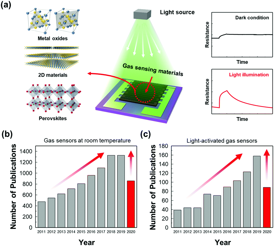 | ||
| Fig. 1 (a) Schematic of the light-activated gas sensor. Results from a Web of Science literature survey for articles about (b) gas sensors operating at low temperatures and (c) light-activated gas sensors from 2011 to July, 2020. Web of Science [v.5.35] Core Collection Search keywords: (b) TS = gas sensor AND (TS = room temperature OR TS = low temperature) and (c) TS = gas sensor AND (TS = room temperature OR TS = low temperature) AND (TI = UV OR TI = ultraviolet OR TI = light OR TI = illumination OR TI = LED OR TI = photo OR TI = irradiation). | ||
The most widely accepted mechanism for the chemoresistive gas sensors is the oxygen absorbate-mediated electric interaction.48 The oxygen molecules get adsorbed onto the surface of semiconductors in three ionized states (O2−, O−, or O2−) depending on the operating temperature.49 According to N. Barsan and U. Weimar, the molecular form (O2−) dominates ionosorption at a temperature below 150 °C and the atomic form (O− or O2−) dominates at a temperature over 150 °C.34 Although oxygen molecules (O2(gas)) have a very low chance of ionosorption at room temperature, several studies have experimentally confirmed the ionized oxygen molecules (O2(ads)−) on the surface of semiconductors at room temperature. B. Liu et al. and L. Liu et al. measured the conductivity of the semiconductors under either pure O2 and pure N2 without any external heating or photo-activation, indicating ionosorption of O2.50,51 Therefore, the light-activated gas sensors operating at room temperature are also expected to have oxygen absorbate-mediated gas sensing mechanisms, and most of the previously reported papers also interpret their gas sensing properties through oxygen absorbates. Fig. 2 summarizes the oxygen adsorption process under dark and light irradiated conditions. Under the dark conditions, the oxygen adsorption follows the conventional mechanism that molecular oxygen (O2(ads)−) adsorbs onto the surface. Under light irradiation, photogeneration of electrons and holes takes place. The photogenerated holes (h(photo)+) interact with adsorbed molecular oxygen (O2(ads)−) to desorb them from the surface (h(photo)+ + O2(ads)− ↔ O2(gas)). The exposed reactive sites after desorption of oxygen can be considered advantageous to gas sensing reactions due to an increased number of reactive sites.52 The released oxygen and the pre-existed oxygen react again with photogenerated electrons (e(photo)−) to adsorb molecular oxygen again (O2(gas) + e(photo)− ↔ O2(photo)−). The photo-adsorbed oxygen molecules (O2(photo)−) are expected to weakly bound to semiconductors and be more reactive than naturally ionosorbed oxygen molecules (O2(ads)−), which are thermodynamically stable and less reactive at room temperature.53 Therefore, overall gas sensing kinetics and gas responses can be accelerated under light irradiation. The photo-adsorbed oxygen molecules then react with target gas molecules. For example, NO2, the most notable oxidizing gas, takes electrons away from photo-adsorbed oxygen to increase the resistance in the case of n-type semiconductors (NO2 + O2(photo)− ↔ NO2(ads)− + O2(gas)). For reducing gases like CH3COCH3, electrons are transferred from reducing gases to semiconductors with products of CO2 and H2O (CH3COCH3 + 4O2(photo)− ↔ 3CO2 + 3H2O + 4e−), resulting in a decrease in the resistance in the case of n-type semiconductors.
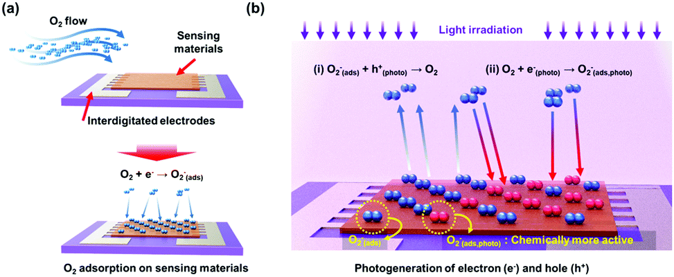 | ||
| Fig. 2 Schematic of the oxygen adsorption process under (a) dark condition and (b) light irradiated conditions. | ||
3. Light-activated gas sensing properties of semiconductors
3.1 Metal oxides
The metal oxide semiconductors, such as SnO2, WO3, ZnO, NiO, Co3O4, or In2O3 have been one of the most widely adopted gas sensing materials.54–59 The current commercially available gas sensors are mostly based on metal oxide semiconductors due to their earth-abundant availability and cheap price.60 The metal oxide semiconductors also have strength in the detection of various volatile organic compounds (VOCs) at a low concentration, which is essential for indoor air monitoring.48,61 However, as mentioned before, their high operating temperature over 250 °C has been the most significant hurdle to be applied to mobile devices due to high power consumption. Although some companies have been successful in reducing power consumption through pulsed voltage application, it is still not enough to fulfil the requirements for IoE applications.62 Therefore, alternative methods like light activation have been highly demanded.In the aspect of the light activation, most of the metal oxide semiconductors have bandgap energies higher than 3.0 eV, which is in the ultraviolet (UV) range.63 Therefore, most of the light-activated gas sensors based on metal oxides utilize UV light as an activation source. B. Liu et al. reported the UV light-activated gas sensing properties of SnO2 nanosphere array films.50Fig. 3a shows a cross-sectional scanning electron microscopic (SEM) image of the fabricated SnO2 nanospheres. As shown in Fig. 3b, the authors illuminated UV light to a monolayer of SnO2 nanospheres with different light intensities to find the optimal intensity, while 10 ppm NO2 was injected into the chamber. The optimal intensity was 3.09 mW cm−2 and the gas sensing response was significantly enhanced compared to that under dark conditions. Under the illumination of the optimized UV light intensity, the SnO2 nanosphere with a different number of layers has been prepared and exposed to different concentrations of NO2 (Fig. 3c–f). All the sensors exhibited a perfect linear relationship to the target gas. The gas responses and sensitivity (the slope of the graph in response to concentration relationship) were all highest for the SnO2 nanospheres with 4 layers under UV light illumination. Under the same intensity of light illumination, the top layers absorb most of the illuminated light and the bottom region absorbs a little of it. Therefore, the SnO2 nanospheres with 6 layers were too thick to utilize UV light illumination for gas sensing reactions and 4 layers were the optimal thickness for the reaction. The optimized SnO2 nanosphere with 4 layers exhibited NO2 selectivity, which is expected to have benefited from excessive photogenerated electrons for the reduction of NO2, which consumes electrons unlike reducing gases.
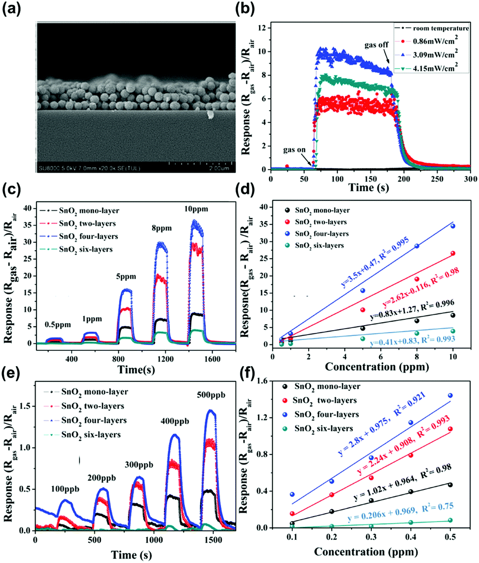 | ||
| Fig. 3 (a) Cross-sectional scanning electron microscopic (SEM) images of the SnO2 array film with tri-layers. (b) Optimum irradiation intensity gas measurement of SnO2 monolayer array film toward 10 ppm NO2. The gas response comparison based on the SnO2 film with different thicknesses toward NO2 in the concentration range of (c) 0.5–10 ppm and (d) the corresponding linear relationships. (e) The same measurements for NO2 concentration range of 100–500 ppb and (f) the corresponding linear relationships. Reproduced with permission from ref. 50. Copyright © 2019 John Wiley & Sons. | ||
X.-X. Wang et al. approached in a way more practical point of view and utilized a polychromatic (white) light source as an activation source.64 The authors fabricated the array of well-aligned In2O3 nanowires on polyimide substrates to achieve flexible and transparent sensors. Fig. 4a–d shows the schematic of the fabricated sensors with optical photographs and SEM images. The fabricated gas sensors based on the In2O3 nanowire array were exposed to 500 ppb NO2 under different light sources at room temperature, as shown in Fig. 4e. Interestingly, the sensors exhibited responses to 500 ppb NO2 under all illuminated light wavelengths including white, blue, green, and red. While gas measurement under green and red light exhibited recovery characteristics and notable gas responses, their response or recovery times were relatively long. In addition, their base resistance in the GΩ range can limit their future practical application due to noisy current. Therefore, the monochromatic blue light and polychromatic white light were chosen for further characterization. The In2O3 gas sensors were then exposed to NO2 of different concentrations under blue light, as shown in Fig. 4f, and their gas responses were plotted as a function of NO2 concentration, as shown in Fig. 4g. The gas response and NO2 concentration exhibited excellent linear relationships, indicating the capability of sensor calibration. The stable operation under blue light irradiation toward 500 ppb NO2 was also confirmed, as shown in Fig. 4h. The same measurements were conducted under white light, as shown in Fig. 4i–k, and they also exhibited a good linear relationship with long-term stability. Then the authors conducted gas sensing measurement under polychromatic light originating from iPhone screen illumination. The iPhone was placed under the chamber with an iPhone screen facing toward In2O3 gas sensors. The distance between sensors and iPhone was 10 cm, and irradiance was measured to be 0.56 W m−2 when the iPhone screen brightness was set at 100%, which is low compared to the white light source used in the measurement (Fig. 4i–k). The iPhone light-illuminated gas sensing toward 500 ppb NO2 exhibited reasonable gas responses and demonstrated potential application and integration of gas sensors with displays of mobile devices.
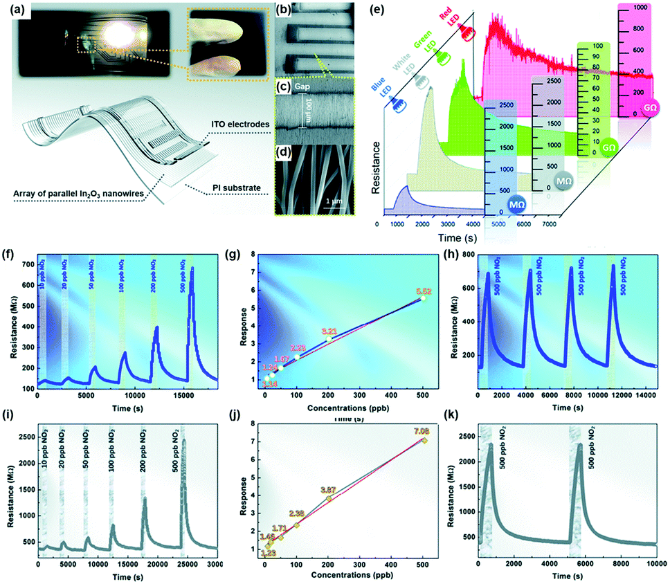 | ||
| Fig. 4 (a–d) Photographs and schematic of flexible and transparent sensors based on an array of parallel In2O3 nanowires: (a) transparent sensor pasted on a bookmark light (with a white LED, 1 W; powered by a 3 V button battery), (b) SEM images of the flexible and transparent sensors based on the In2O3 nanowire array under low magnification, (c) well-aligned nanowires across the electrodes, and (d) parallel In2O3 nanowires under high magnification. (e) Response of the sensor based on the In2O3 nanowire array to 500 ppb NO2 under illumination using different light sources at room temperature. (f–k) Gas sensing properties of the sensor based on the In2O3 nanowire array at room temperature: (f) response–recovery curve of the sensor to different NO2 concentrations, (g) sensor response as a function of NO2 concentration, and (h) response–recovery curve of the sensor to cyclic NO2 exposure under blue LED illumination; (i) response–recovery curve of the sensor to different NO2 concentrations, (j) sensor response as a function of NO2 concentration, and (k) long-term stability (after 180 days and 1000 bendings) under white LED illumination. Reproduced with permission from ref. 64. Copyright © 2020 Royal Society of Chemistry. | ||
Although light illumination on metal oxides was effective in lowering operating temperatures, sensitive and selective detection of VOCs still remains challenging due to their low response even under light illumination.65–67 N. D. Chinh et al. studied gas sensing properties of In2O3 nanostructures under UV light illumination at room temperature.68 The measurement toward various gases also revealed highly sensitive behavior to NO2 like other reports while exhibiting low gas responses toward VOCs. According to authors, UV illumination is effective in the generation of charge carriers for photocatalytic enhancement of gas sensing characteristics; its effect on chemical reactions occurring on the surface is much smaller than the temperature effect. Especially, the chemical reaction of reducing gases (C2H5OH, CH3COCH3, HCHO, or CH4), which has water molecules as a product, cannot overcome water formation energy through supplied energy from UV illumination. Through UV illumination, adsorption and desorption of gas molecules can be significantly promoted and selective detection of oxidizing gases like NO2 and NO can be effectively achieved. Therefore, for the selective detection of VOCs with light activation of metal oxides, other systematic strategy to amplify low gas responses toward VOCs is highly demanded.
R. Jaisutti et al. reported amorphous indium-gallium-zinc oxide (IGZO) as one of those strategies to overcome low selectivity toward VOCs.69 Compared to other polycrystalline metal oxides that need to have inevitable Schottky barriers at grain boundaries, amorphous metal oxides can avoid the formation of Schottky barriers and promote efficient charge transport in the gas sensing layers. Fig. 5a and b show the schematic of the fabrication process and a photograph of the final device of IGZO gas sensors prepared on indium-tin-oxide (ITO) interdigitated electrodes. Fig. 5c shows the optical transmittance spectra and the Tauc plot for the IGZO gas sensors. The bandgap energy was calculated to be 3.19 eV, and this large bandgap contributed to high optical transmittance of the IGZO gas sensors. Fig. 5d shows the overall response current behavior of IGZO gas sensors toward UV illumination and acetone exposure. Under the dark condition, IGZO gas sensors did not exhibit any gas response toward 750 ppm CH3COCH3 due to the low electric conductivity of the IGZO and insufficient energy to overcome the activation energy of ionosorbed oxygen species.70 Under UV illumination, photogenerated electron and hole pairs increased the conductivity of the IGZO film, and photocurrent was significantly enhanced, as shown in Fig. 5d. In addition, as mentioned before, photogenerated electron and hole pairs participate in photocatalytic adsorption of oxygen as loosely bound active sites, and this induced saturation curves before exposure to CH3COCH3. Upon exposure to CH3COCH3, photo-catalytically adsorbed oxygen species participate in the chemical reaction (CH3COCH3 + 4O2(photo)− ↔ 3CO2 + 3H2O + 4e−) to release additional electrons to increase the conductivity of IGZO film. The IGZO gas sensors were then exposed to 750 ppm CH3COCH3 under UV light with different intensities (1 to 30 mW), as shown in Fig. 5e. With the increase in UV intensities, the increased number of photogenerated electron and hole pairs can participate in photocatalytic adsorption of oxygen species and those loosely bound oxygen absorbates can enhance the gas sensing response of IGZO gas sensors toward CH3COCH3. Compared to the polycrystalline metal oxide, the amorphous IGZO film was beneficial in the transport of photogenerated charge carriers and efficient photocatalytic adsorption was available. The sensitivity (defined as (output current change)/(initial current) × 100%) is summarized as a function of the UV power intensity, as shown in Fig. 5f, and they exhibit a good linear relationship. The energy band bending according to the above-mentioned mechanisms is illustrated in Fig. 5g. The photogenerated electrons cause band bending at the surface and promote photocatalytic oxygen adsorption under ambient air. The IGZO gas sensors were exposed to various VOCs gases, including CH3OH, C2H5OH, CH3CHOHCH3, CH3COCH3, C7H8, and C6H5Cl. As a result, the IGZO sensors exhibited sensitive behaviors to a group of alcohols (CH3OH and C2H5OH) and low sensitivity toward a group of organic solvents (C7H8 and C6H5Cl).
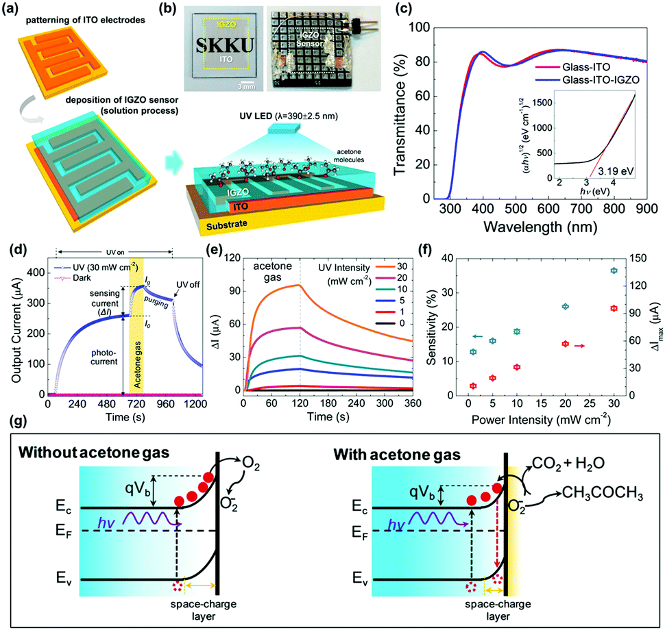 | ||
| Fig. 5 (a) Schematic of the pattern of ITO interdigitated electrodes, solution processing of the IGZO film on the electrodes, and sensing operation under UV-LED irradiation and CH3COCH3 exposure. (b) Optical images of a transparent IGZO sensor before and after bonding on a print circuit board. (c) Optical transmittance spectra (inset shows that the Tauc plot exhibited the band gap of the IGZO film). (d) Overall response current behavior (I vs. t) of an IGZO gas sensor operated under a UV intensity of 30 mW cm−2 and a CH3COCH3 concentration of 750 ppm. (e) Gas sensing properties of UV-activated IGZO gas sensors operated under different UV intensities (1 to 30 mW cm−2, with a CH3COCH3 concentration fixed at 750 ppm). (f) Current change (ΔI) and gas sensitivity during CH3COCH3 exposure at different UV intensities. (g) Schematic showing the energy band bending under photoinduced oxygen ions without (left) and with (right) interaction of CH3COCH3 molecules at the IGZO surface. Reproduced with permission from ref. 69. Copyright © 2016 American Chemical Society. | ||
There have been other various strategies to overcome the low selectivity of metal oxide semiconductors under light illumination (mostly UV light) at room temperature, including formation of heterojunctions71–73 or catalyst decoration.74,75 Despite these efforts, the highest gas responses were usually exhibited when exposed to oxidizing gases like NO2 or NO and selective detection of VOCs remains challenging for the light-activated gas sensors based on metal oxides. As N. D. Chinh et al. explained, not enough energy supplied by light illumination to overcome water formation energy, which is the product of VOCs sensing reaction, is the primary reason for the low VOC selectivity.68 As a result, the highly selective behavior only to oxidizing gases has been mainly reported by light-activated gas sensors based on metal oxides. The further strategies and efforts on the enhancement will be described in the later section of this review.
3.2 Two-dimensional materials
Two-dimensional materials including graphene,76 graphene derivatives,77–79 or transition metal dichalcogenides (TMDs)80,81 have been one of the most attracted materials for gas sensors operating at room temperatures. The 2D materials exhibit a high surface-to-volume ratio and a high surface energy, which are beneficial for adsorption and desorption of target gas molecules even at room temperature. While graphene and its derivatives are intrinsically metallic and have difficulties in opening a gap at the Dirac cone to limit their utilization of excellent electronic properties, TMDs including MoS2, WS2, and SnS2 are intrinsic semiconductors with distinct bandgaps for easy application to various electronic devices.82 In particular, in the aspect of light activation, TMDs with distinctive bandgap energies smaller than metal oxides can enable activation under visible light. Although a previously addressed work of X.-X. Wang et al. successfully demonstrated the light-activated gas sensing characteristics under the illumination of the iPhone screen, the light-activation heavily rely on a short wavelength region of polychromatic white light.63 If visible light can be used as an activation source, all the light sources available during human life can be used as activation sources, leading to more practically reasonable light-activated gas sensor technologies. The utilization of visible light sources can also prevent potential damages to sensing materials caused by UV light via generation of ozone in an oxygen-rich atmosphere.83D. Gu et al. fabricated gas sensors based on WS2 microflakes for the detection of VOCs under light illumination with different wavelengths.84Fig. 6a shows the SEM image of the prepared WS2 samples with a typical layered flake morphology. The microflake size varies from 1 μm to 4 μm. Fig. 6b shows the response curves of the WS2 microflakes under light illumination with different wavelengths (365, 525, 580, 850, and 940 nm) and dark conditions toward 10 ppm NH3. The operating temperature was 40 °C and the relative humidity condition was 30%. Compared to the gas response under dark conditions, all light-illuminated gas responses exhibited higher values, indicating the capability of visible light absorption by prepared WS2 microflakes. Among various wavelengths, 365 nm light illumination exhibited the highest gas response with the fastest kinetics. The light illumination with longer wavelength exhibited slightly lower gas responses except for 940 nm. A shorter wavelength with a higher energy will certainly be capable of excitation and photocatalytic oxidation at a higher rate than the longer wavelengths, corresponding to lower gas responses for longer wavelengths. The unexpectedly high gas response under 940 nm light illumination may be related to inconsistent light intensities for each light wavelength that authors did not mention in the manuscript, still these data show the capability of light activation of WS2 microflakes by visible light wavelength. Fig. 6c shows the resistance curves of the WS2 microflakes under light illumination with 365 and 940 nm and dark conditions toward 5–60 ppm NH3. The responses toward different concentrations of NH3 are summarized as a function of NH3 concentration in Fig. 6d. These curves well support stable operation under visible light operation with excellent correlation curves, indicating the capability of sensor calibration. The gas sensing mechanism follows that of metal oxides having photocatalytic oxygen adsorption and its high reactivity as primary contributing factors.
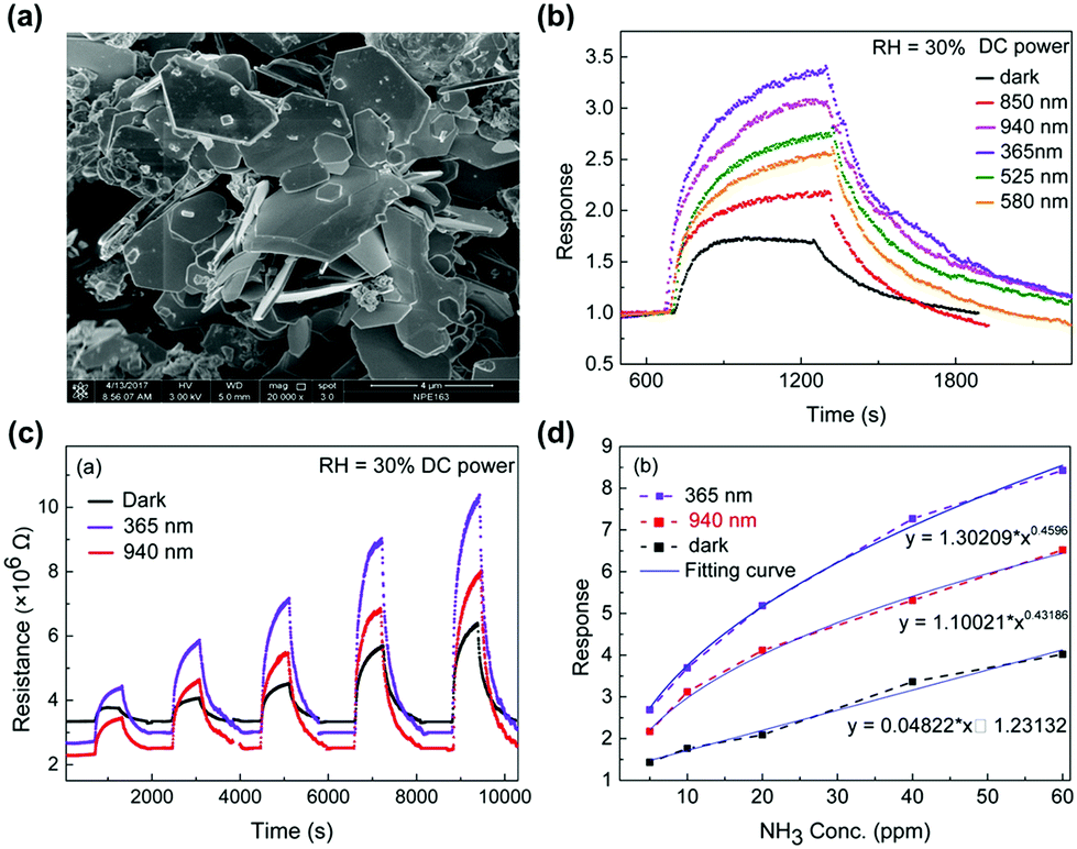 | ||
| Fig. 6 (a) SEM images of the as-milled WS2 sample. (b) Response curves of the WS2-based chemoresistive sensors under different light illuminations driven by DC power to 10 ppm NH3. (c) Comparison of the resistance curve of the WS2-based sensor under light (365 nm, 940 nm) illumination driven by DC power and the darkness to NH3 from 5 to 60 ppm. (d) Correlation curve of the response of the sensor under the light (365 nm, 940 nm) illumination and the darkness. Reproduced with permission from ref. 84. Copyright © 2017 Elsevier B. V. | ||
Another work by D. Gu et al. demonstrated visible light-activated gas sensing characteristics of SnS2 nanosheets.85Fig. 7a shows a SEM image of the prepared SnS2 nanosheets with typical layered structures with a size in the range of 50–200 nm. Fig. 7b shows the I–V polarization curves of the SnS2 nanosheets under irradiation at different wavelengths. The I–V characteristics of SnS2 nanosheets exhibit ohmic behaviors with a higher conductivity for the SnS2 nanosheets under light illumination at shorter wavelengths. Considering the widely reported bandgap of SnS2 (2.36 eV), the green wavelength corresponds to the bandgap energy, and the I–V characteristic at a longer wavelength than the green wavelength exhibited relatively low conductivity, indicating less light activation.86,87 The fabricated SnS2-based gas sensors were exposed to 1–8 ppm NO2 under green light illumination at room temperature, and the gas response curves are shown in Fig. 7c. The gas response and gas concentrations exhibit a nearly linear relationship with stable operation and excellent recovery characteristics. Interestingly, the authors compared the gas selectivity of SnS2 nanosheets toward various gases under both green light illumination at room temperature and high operating temperature conditions without any light illumination (Fig. 7d). The overall gas selectivity under both activation modes (optical and thermal activations) exhibited almost the same selective behavior with similar gas responses. These results indicate that there was no significant influence on the choice of activation modes for the gas sensing characteristics of SnS2 nanosheets. Although limited selective behavior only to NO2 could not be improved even by adopting TMDs as sensing channels for the light-activated gas sensors, nearly the same selective behavior under both optical and thermal activation modes implies selective distinguish between each VOC can be more capable by using TMDs than metal oxides under visible light illumination.
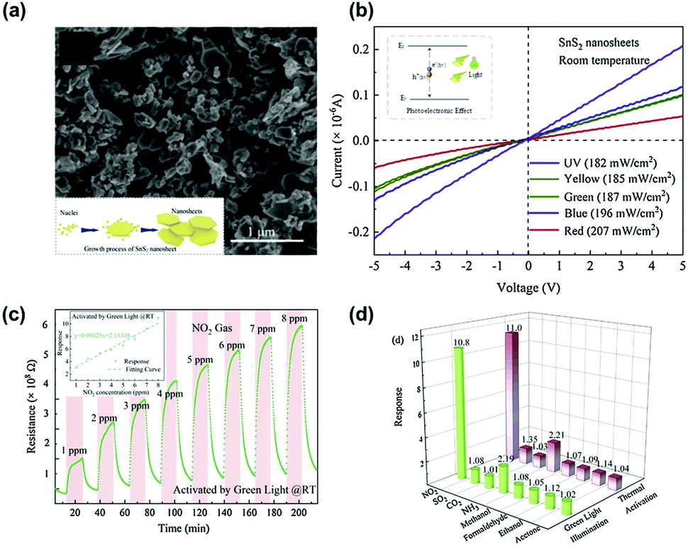 | ||
| Fig. 7 (a) SEM image of the as-synthesized SnS2 nanosheets. (b) I–V polarization curves of the SnS2-based sensor under different light sources. (c) Resistance of the as-fabricated SnS2-based sensor to 1–8 ppm NO2 concentrations and the correlation curve (inset) under green LED light activation at room temperature. (d) Selectivity of the sensor under two activation modes (green LED light and thermal activation) (CO2: 30 ppm; the other interferent gas: 10 ppm). Reproduced with permission from ref. 85. Copyright © 2020 Elsevier B. V. | ||
Y. Huang et al. reported SnS2/rGO nanohybrids with p–n transition for the visible light-activated gas sensors.88 The heterojunction between two different 2D materials can exhibit light-activated gas sensing properties that cannot be expected from a single material. The authors controlled a ratio of rGO to manipulate the conduction type of SnS2/rGO nanohybrids to either n-type or p-type conduction through one-step hydrothermal methods. Fig. 8a shows the schematic illustration of the synthesis procedure of SnS2/rGO nanohybrids. SnS2 is an n-type semiconductor and the high composition ratio of rGO can result in p-type semiconducting characteristics. Fig. 8b–e shows the structural characterizations of n-type and p-type SnS2/rGO nanohybrids. The rigid hexagonal SnS2 layers and lamellar structure of rGO can be confirmed through SEM images. The gas sensors were fabricated by drop-casting the synthesized SnS2/rGO nanohybrids on interdigitated electrodes (IDEs) with patterned alumina substrates. Before light illumination, the gas sensing properties of SnS2 with varying rGO ratios were tested through exposure to NO2. Pure SnS2 exhibited almost no gas response to NO2 at room temperature, but the addition of 1 mg rGO resulted in a significant increase in gas responses (255%). This can be attributed to promoted charge transport from SnS2 to rGO through the sp2 orbital of rGO. After the addition of 5 mg rGO, SnS2/rGO was converted from n-type into p-type conduction with a gas response of 47% toward 1 ppm NO2, and pure rGO exhibited almost negligible gas response toward NO2. The heterojunctions between SnS2 and rGO facilitated gas sensing at room temperature even without light illumination. To investigate light-activated gas sensing characteristics of SnS2/rGO nanohybrids, blue (450 nm), green (532 nm), and red (650 nm) light illumination was conducted with varying intensities (1, 3, 5, 30, and 80 mW cm−2) during exposure to NO2. The p-type SnS2/rGO nanohybrids exhibited almost no enhancement through light illumination since rGO is not a good photoelectric material and cannot provide sufficient photogenerated charge carriers due to the very small bandgap. However, n-type SnS2/rGO nanohybrids exhibited dramatically enhanced gas sensing characteristics upon light illumination. In Fig. 8f–h, the amplification factor (defined as (sensitivity at light)/(sensitivity at dark)), relative response time (defined as (response time at light)/(response time at dark)), and relative recovery time (defined as (recovery time at light)/(recovery time at dark)) of SnS2/rGO nanohybrids are summarized. Interestingly, the highest amplification factor was observed for the lowest light intensity. These results indicate that there is an optimal light intensity for the gas sensing reaction, which are in accordance with the previous reports on metal oxides and MoS2.89–91 One of the possible reasons is that the number of photogenerated charge carriers that participate in the gas sensing reaction can decrease at an excessively high light intensity. Another possible reason is that the desorption reaction can dominate the adsorption reaction at an excessively high light intensity. The illuminated three wavelengths exhibited almost similar effects on gas sensing properties including gas responses as above, response times, and recovery times. The response time increased under all light illuminating conditions, while the recovery time was shortened at a low intensity and delayed at a high intensity. These can be attributed to direct photoexcitation of the electrons from NO2 into the conduction band, and intensity-dependent desorption processes. Fig. 8i–k shows the proposed band alignment diagrams at the heterojunctions of SnS2/rGO nanohybrids regarding the descriptions above.
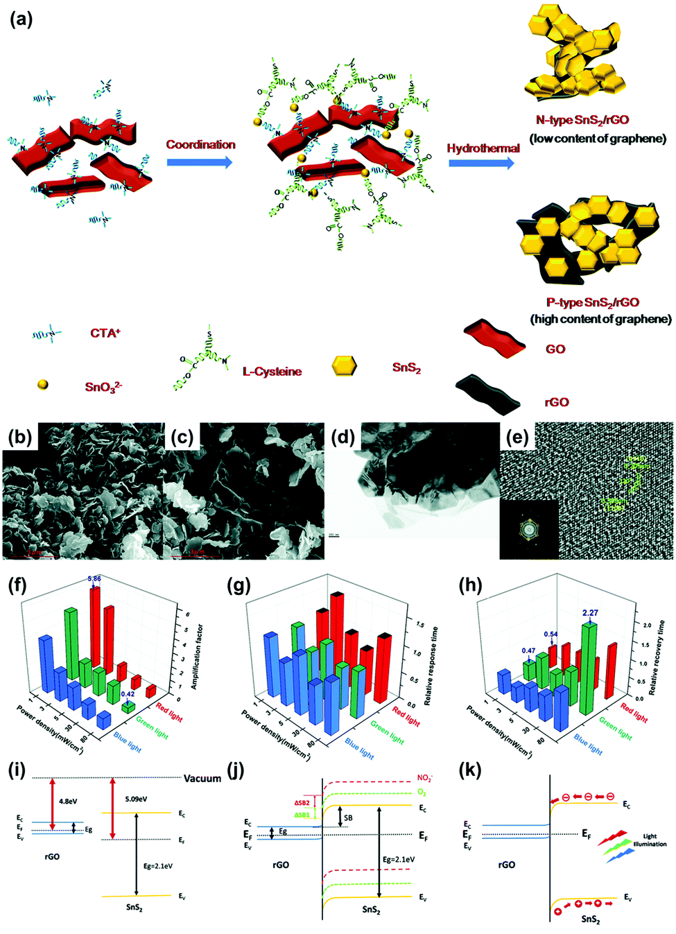 | ||
| Fig. 8 (a) Schematic of the process of hydrothermal synthesis of SnS2/rGO nanohybrids. SEM image of (b) n-type and (c) p-type SnS2/rGO nanohybrids. (d) TEM image of SnS2/rGO nanohybrids. (e) HRTEM image of SnS2 and the resulting FFT pattern (inset). (f–h) The effect of light illumination on the gas sensing properties of n-type SnS2/rGO sensors. (f) The amplification factor of sensitivity under light illumination of different wavelengths and power densities. (g) The relative response and (h) recovery times under light illumination of different wavelengths and power densities. (i–k) Proposed band alignment diagrams at the SnS2/rGO junctions. (i) Energy diagram of the SnS2 and rGO before forming hybrids. (j) Band realignment and energy diagram of n-type SnS2/rGO sensors and the formation of the Schottky barrier. Yellow, green and red lines indicate the energy band of the pristine n-type SnS2/rGO sensors (solid yellow), after exposure to O2 (dashed green) and after exposure to NO2 (dashed red), respectively. ΔSB1 and ΔSB2 represent the Schottky barrier shifted by the O2 and NO2, respectively. The light illumination will change the height of ΔSB1and ΔSB2 to affect the sensing behavior. (k) The band alignment diagram of the light-assisted SnS2/rGO sensors. Reproduced with permission from ref. 88. Copyright © 2019 The Royal Society of Chemistry. | ||
As explained, the 2D materials are capable of the activation under visible light illumination and prevention of possible damages that can be caused by UV light illumination.83 In addition, the utilization of visible light wavelength can provide more chance of practical application by taking advantage of numerous light sources available in everyday life. However, lacking selectivity toward VOCs still remains challenging as it was for metal oxides under light illumination at room temperature, and further studies are highly demanded to overcome it.92,93
3.3 Other materials
While metal oxides and 2D materials are the most widely studied electronic materials for the gas sensor application, there have been other efforts on discovering new possible electronic materials for the gas sensors including inorganic halide perovskites,40,41 metal sulfides,42,94–100 and organic semiconductors.53,101–103 This section summarizes the light-activated gas sensing properties of electronic materials other than metal oxides and 2D materials.A. Tricoli's group has first reported light-activated gas sensing properties of CsPbBr3 and CsPbBr2I inorganic halide perovskites.40,41 Unlike organic–inorganic hybrid perovskites suffering unstable operation and being stable under ambient air, inorganic halide perovskites which have Cs atoms as substitutes for organic cations can secure their stability to function as gas sensors. Fig. 9a shows the schematic of O2 sensing by CsPbBr3-based gas sensors. The cross-sectional SEM image in Fig. 9b indicates a CsPbBr3 film with 350 nm thickness deposited on a fluorine-doped tin oxide (FTO) glass. Upon exposure to the oxidizing gas of O2 at room temperature under the illumination of 420 nm visible light, highly sensitive detection of O2 was available, as shown in Fig. 9c. Compared to the dynamic response of CsPbBr3 to O2 having almost no response, visible light illumination resulted in a gas response of 0.93 with extremely fast response time (17 s) and recovery time (127 s), which are difficult to achieve with other materials at room temperature. Fig. 9d shows the dynamic response curves of CsPbBr3 to four consecutive pulses of O2 under visible light illumination. The CsPbBr3 exhibited stable operation upon multiple exposures with consistent gas responses. Interestingly, when CsPbBr3 is exposed to reducing gases such as C2H5OH and CH3COCH3, the current level also increases as it does for oxidizing gases. This indicates that a somewhat different gas sensing mechanism takes place for CsPbBr3 compared to conventional semiconductors such as metal oxides and 2D materials. The authors emphasize that halide perovskites are ambipolar charge transporters due to the similarity of electron and hole effective mass.104,105 Based on the ambipolar properties of CsPbBr3, the authors propose that O2, C2H5OH, and CH3COCH3 function as vacancy fillers and reversibly fill in intrinsic Br vacancies of the CsPbBr3. Considering Br vacancies can trap the photogenerated charge carriers, the decreased number of Br vacancies after being filled in by the introduced target gas molecules results in an increase in the free photogenerated charge to increase the current level of CsPbI3. Fig. 9e shows the schematic of VOC sensing by CsPbBr2I under light illumination. CsPbBr2I has a broader absorption range than CsPbBr3, and therefore, it can be expected to exhibit different gas sensing characteristics from CsPbBr3. Fig. 9f shows the cross-sectional SEM image of the CsPbBr2I film deposited on the FTO glass. Upon exposure to CH3COCH3 gas at room temperature under solar irradiation (AM 1.5, 42.3 mW cm−2), CsPbBr2I exhibited highly sensitive detection of CH3COCH3, while there is almost no response under dark conditions, indicating that photogenerated charge carriers play a critical role in gas sensing (Fig. 9g). Fig. 9h shows the stable operation of CsPbBr2I toward two consecutive pulses of CH3COCH3 under light illumination. Similar to CsPbBr3, CsPbBr2I also exhibited a current increase upon exposure to both oxidizing gases and reducing gases, implying different gas sensing mechanisms from conventional semiconductors. Fig. 9i shows an energy band diagram of the CsPbBr3I gas sensors. Upon light illumination, photogenerated electrons transfer from the conduction band of CsPbBr2I to the FTO glass across the hole blocking layer, and the photogenerated holes transfer from the valence band of CsPbBr2I to the Au probe.106,107 As a result, the net current flow through the out circuit can be formed from the FTO glass to Au without any external ways. This current flow can be used to transduce the electrical characteristics upon exposure to target gas molecules. Fig. 9j illustrates the possible gas sensing mechanism of CsPbBr2I gas sensors. In a N2 atmosphere without any target gas molecules, recombination of photogenerated electrons and holes can take place at trap sites like vacancies. Any existence of O2 like ambient air can passivate the trap sites to reduce recombination, increasing the current level. In other words, the presence of O2 in the atmosphere can reduce active sites for target gas molecules to decrease sensor responses, as shown in Fig. 9g. Similarly, the introduction of target gas molecules like VOCs in the N2 atmosphere can passivate the trap sites of CsPbBr2I to reduce the recombination and increase the current level to function as gas sensors. These unique gas sensing properties and mechanisms of inorganic halide perovskites reported by A. Tricoli's group can provide a new insight toward the design of low-power consuming gas sensors.
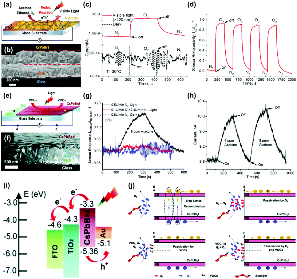 | ||
| Fig. 9 (a) Schematic of O2 gas sensing by a CsPbBr3-based chemical sensor device. (b) Cross-sectional SEM image of an exemplary CsPbBr3 film deposited on an FTO glass substrate. (c) Dynamic responses of a typical CsPbBr3 sensor to switching the chemical environment from pure N2 to pure O2 in dark (broken line) and under visible-light illumination (red line). (d) Stability of the CsPbBr3 gas sensor response to the pure N2/O2 atmosphere switching under four consecutive cycles under visible-light illumination. (e) Schematic of the CsPbBr2I chemical sensor layout. (f) Cross-sectional SEM image of a representative CsPbBr2I film deposited on a compact TiO2 layer on a FTO glass substrate. (g) Dynamic CsPbBr2I sensor response to injection of 8 ppm CH3COCH3 in pure N2 (black line) and simulated air (red line) under simulated solar irradiation (AM 1.5, 42.3 mW cm−2), and in pure N2 under darkness (blue line). (h) Photocurrent response kinetics of a CsPbBr2I sensor to injection of 4 and 8 ppm CH3OCH3 in pure N2. (i) Energy level diagram of the CsPbBr2I device. (j) Schematic of the CsPbBr2I chemical sensing mechanism. Reproduced with permission from ref. 40 and 41. Copyright © 2017 John Wiley & Sons. Copyright © 2019 Royal Society of Chemistry. | ||
H.-Y. Li et al. reported light-activated gas sensing properties of CdS taking advantage of its low bandgap (∼2.4 eV) and resistance.42 The low bandgap enables visible light absorption by CdS. The authors synthesized 2D CdS nanoflake arrays using chemical vapor deposition methods and investigated NO2 sensing characteristics under illumination by a fluorescent lamp and solar light at room temperature. Fig. 10a–d show the structural characterizations of the synthesized CdS nanoflake arrays. Hexagonal CdS nanoflakes with 10–20 nm thickness with a densely packed bottom region and a loosely packed top region can be confirmed. Therefore, highly porous nanostructures could be formed at the top surface, which is beneficial for the accessibility of target gas molecules. Fig. 10e shows the I–V curves of CdS nanoflake arrays under different light sources in ambient air. The CdS nanoflake arrays reacted to all light wavelengths with their highest response to blue wavelengths. The response toward UV light was lower than that toward blue light, and this can be attributed to a lower light intensity and a relatively high recombination rate that originated from the excessively high photon energy. Upon exposure to 5 ppm NO2 under the illumination of different light sources, CdS nanoflake arrays exhibited varying gas sensing characteristics, as shown in Fig. 10f. The gas responses of CdS nanoflake arrays were highest under red wavelength, but the recovery characteristics were not impressive. The response and recovery were fast under blue and green wavelengths, while the gas response was higher under green wavelength than under blue wavelength. The gas response was the lowest under UV illumination. Collectively, the authors chose green light as an optimal light source to activate gas sensors based on CdS nanoflake arrays. Fig. 10g shows the gas sensing curves of CdS nanoflake arrays under irradiation by various green light sources. Although gas responses were highest under the lowest irradiance of 2.5 W m−2, the gas response under 21 W m−2 irradiance was still enough to distinguish the sensor signals, and highly promoted response time and recovery time under 21 W m−2 were considered important for the potential real application. The various measurements under optimized conditions exhibited highly sensitive and selective behaviors toward NO2 gas with an excellent linear relationship between the gas response and NO2 concentrations, indicating the capability of sensor calibration. The authors also demonstrated light activation under natural solar light irradiation, which exhibited acceptable light-activated gas sensing properties. The gas sensing mechanism follows conventional gas sensing models for light-activated gas sensors that are mentioned in the previous sections. The application of low-bandgap materials such as CdS can utilize visible light illumination as an activation source and reduce any potential damage induced when using light with high photon energy.
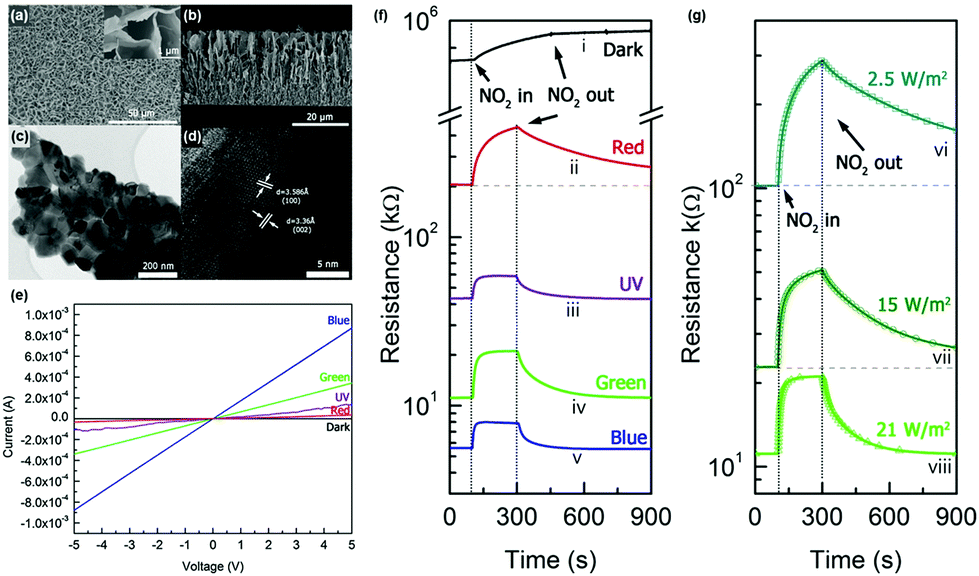 | ||
| Fig. 10 (a) Top-view and (b) cross-sectional view SEM image (c) and high-resolution TEM image (d) of the CdS nanoflake array gas sensor. (e) I–V curves of CdS nanoflake arrays under different light sources in air. (f and g) CdS nanoflake arrays sensor's response to 5 ppm NO2 (f) under different light sources and (g) various green LED irradiance. Reproduced with permission from ref. 42. Copyright © 2018 Elsevier B. V. | ||
X. Tian et al. reported the utilization of perylenediimide on SnO2 for the visible light-activated gas sensing properties.53 The perylenediimide is an n-type organic semiconductor that has the high planarity of large conjugated systems, resulting in extremely high chemical, thermal, and optical stability under visible light illumination.108–110 While pristine SnO2 can only be activated under UV irradiation, the introduction of perylenediimide enables the activation under visible light illumination. Fig. 11a shows the SEM image of pristine SnO2 films and Fig. 11b and c show the SEM images of the perylenediimide-sensitized SnO2 film. Perylenediimide exhibits a morphology of fibril structures induced by the strong π–π stacking interaction between perylenediimide skeletons along the long axial direction. Perylenediimide formed network structures on the surface of the SnO2 film. Fig. 11d and e show the dynamic response curves of perylenediimide-sensitized SnO2 and pristine SnO2 toward 0.5 ppm NO2 under the dark and light-illuminated conditions, respectively. The gas sensing reaction and recovery to baseline resistance under dark conditions take more than an hour for both samples, which is not practical at all. However, they were dramatically shortened under visible light illumination to a time scale of several minutes (response time of 6 min and recovery time of 4 min, respectively). The overall gas responses of perylenediimide-sensitized SnO2 were also significantly increased to 131.60, which is 4 times higher than that under dark conditions. Fig. 11f shows the dynamic response curves of perylenediimide-sensitized SnO2 to different concentrations of NO2 (250 ppb–4 ppm), and Fig. 11g shows the corresponding gas responses as a function of NO2 concentrations. The gas responses and NO2 concentrations exhibit an excellent linear relationship, indicating the capability of sensor calibration. Upon exposure to various gases, the perylenediimide-sensitized SnO2 exhibited highly sensitive and selective detection of NO2 under visible light illumination. The gas sensing mechanism also follows the conventional model for the light-activated gas sensors that are explained earlier in this review. The utilization of organic semiconductors with low-bandgap energy to metal oxides can facilitate visible light absorption to prevent potential disadvantages caused by UV illumination.
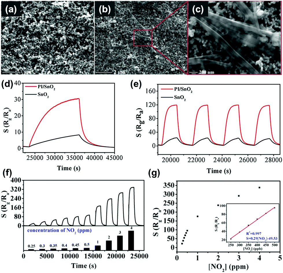 | ||
| Fig. 11 (a) SEM image of the SnO2 film. (b and c) SEM images of the perylenediimide-sensitized SnO2 hybrid film. (d and e) Dynamic response curves of perylenediimide-sensitized SnO2 and pure SnO2 towards 0.5 ppm NO2 (d) without and (e) with visible-light illumination. (f) Dynamic response curves of perylenediimide-sensitized SnO2 to different concentrations of NO2 (250 ppb–4 ppm). (g) The corresponding response with different NO2 concentrations. The inset presents the acceptable response at low NO2 concentrations and the linear equation. Reproduced with permission from ref. 53. Copyright © 2019 Elsevier B. V. | ||
4. Various strategies for future applications
4.1 Plasmonic nanoparticles
The most challenging obstacle for the light-activated gas sensors toward further practical application is the lacking sensitivity toward various VOCs other than NO2. The lack of VOC selectivity originates from insufficient activation energy to overcome the water formation energy and promote oxidation of reducing gases under light illumination at room temperature.68 Although various efforts for the utilization of several different materials and their combinations for light-activated gas sensing have been made, the lack of selectivity was difficult to overcome unless the reaction occurs at high operating temperatures. Therefore, incorporation of noble metal nanoparticles (Pt, Au, Ag, Pd, etc.) can be a good strategy since they can promote gas sensing reactions to specific target gas molecules.111–119 Moreover, the noble metal nanoparticles exhibit localized surface plasmon resonance (LSPR) effects under the illumination of resonant wavelengths to supply additional hot electrons to participate in the chemical reaction.F. Xu et al. reported the light-activated gas sensing properties of Au nanoparticles-decorated ZnO nanotetrapods taking advantage of plasmonic resonant energy from Au nanoparticles.38Fig. 12a–d show the schematic of the gas sensor fabrication process. ZnO nanotetrapods were deposited through thermal evaporation on Au electrode-patterned ceramic plates, followed by 5 nm Au sputter deposition and agglomeration into nanoparticles via annealing. Fig. 12e shows the SEM image of pristine ZnO nanotetrapods and Fig. 12f shows the SEM image of Au nanoparticle-decorated ZnO nanotetrapods. The porous network of ZnO nanotetrapods is expected to provide excellent gas molecule accessibility, and the diameter of agglomerated Au nanoparticles ranges from 7 to 50 nm with uniform spatial distribution. Upon exposure to 500 ppm C2H5OH, as shown in Fig. 12g, both pristine ZnO nanotetrapods and Au nanoparticle-decorated ZnO nanotetrapods exhibited almost no gas response at 17 °C. Under white light illumination (6 mW mm−2), pristine samples exhibited a small increase in gas response, whereas Au nanoparticle-decorated samples exhibited dramatically enhanced gas response. The stable operation toward multiple pulses of C2H5OH under light illumination was also confirmed, as shown in Fig. 12h. The Au nanoparticle-decorated ZnO nanotetrapods were then exposed to various VOCs including C2H5OH, CH3COCH3, HCHO, and CH3OH, as shown in Fig. 12i. Under light illumination, gas responses to all gases were dramatically enhanced, and the gas response toward C2H5OH exhibited the highest value. Fig. 12j shows the light-activated gas sensing properties of Au nanoparticle-decorated ZnO nanotetrapods toward different concentration levels of C2H5OH (1–1000 ppm). The gas response and gas concentration exhibited an excellent linear relationship, indicating the capability of practical application. Since the conducting channel of the gas sensors is ZnO, the overall light-activated gas sensing mechanism follows that of conventional metal oxides. In addition to the conventional mechanisms, the decoration of Au nanoparticles increased the Schottky barrier at the interface of Au and ZnO due to a difference in work function, contributing to the suppression of the recombination of photogenerated charge carriers.120 Moreover, under white light illumination that includes 532 nm wavelength, the resonant wavelength for Au nanoparticles can induce LSPR absorption. Therefore, Au nanoparticles can enhance light absorption and broaden the available wavelength range that pristine ZnO cannot achieve.121,122 Through LSPR, highly energetic hot electrons are generated in Au nanoparticles and they can be transported to the conduction band of ZnO through the increased Schottky barrier at the interface. They can participate in the photocatalytic oxygen adsorption process, and localized field enhancement around Au nanoparticles through LSPR can facilitate the generation and separation of photogenerated electron and hole pairs.
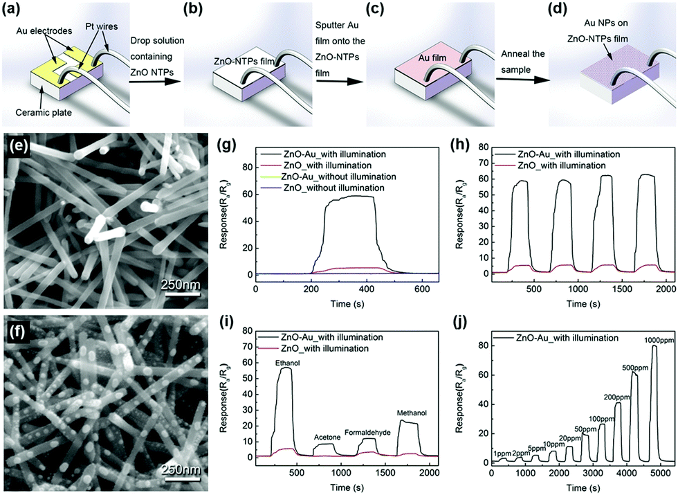 | ||
| Fig. 12 Schematic of the gas sensor fabrication process. (a) Ceramic substrate: two Au pad electrodes pre-deposited on the surface and two Pt wires mounted on the Au electrodes; (b) ZnO deposited on the ceramic substrate; (c) 5 nm Au film covered ZnO-based sensor; (d) final sensor device with ZnO decorated with Au NPs. (e and f) SEM images of the sensor devices with (e) pure ZnO and (f) Au NP-decorated ZnO. (g–j) Real-time sensing response curves of sensors made of pure ZnO and Au NP-decorated ZnO at 17 °C. (g) Exposure to 500 ppm C2H5OH. (h) Cyclic repeated exposure to 500 ppm C2H5OH under white light illumination. (i) Sequential exposure to 500 ppm of different gases including C2H5OH, CH3COCH3, HCHO and CH3OH with devices under white light illumination. (j) Exposure to different concentration levels of C2H5OH vapor (1–1000 ppm) with devices made of Au NP-decorated ZnO under white light illumination. Reproduced with permission from ref. 38. Copyright © 2018 Elsevier B. V. | ||
R. Chen, et al. prepared oxygen vacancy-enriched ZnO nanorod/Pd nanoparticle hybrids for light-activated gas sensing.39 The authors treated ZnO nanorods with H2 (10% in Ar) to realize oxygen vacancy-enriched nature, followed by the dispersion of Pd nanoparticles by a solvent reduction method. Fig. 13a and b show the transmission electron microscopic (TEM) images of the normal ZnO/Pd hybrid and the oxygen vacancy-enriched ZnO/Pd hybrid, respectively. Although oxygen vacancies cannot be distinguished in the TEM images, uniformly distributed Pd nanoparticles on ZnO nanorods can be confirmed. The existence of oxygen vacancies was confirmed by X-ray photoelectron spectroscopy analysis through increased oxygen vacancy peaks. Fig. 13c and d show the dynamic response curves of each fabricated gas sensor toward 0.1% CH4 under the dark and 590 nm light-illuminated conditions (6 mW cm−2), respectively. The corresponding gas response values are summarized in Fig. 13e. The pristine ZnO nanorods and oxygen vacancy-enriched ZnO nanorods did not exhibit any gas response to CH4, well-known chemically inert explosive gas, under both dark and light-illuminated conditions.123 This indicates that oxygen vacancy alone cannot contribute to the light-activated CH4 sensing at low temperatures. ZnO/Pd hybrids without oxygen vacancy enrichment exhibit a little gas response under the dark condition and a slightly increased gas response under light-illuminated conditions. The dispersion of Pd nanoparticles was effective in promoting CH4 sensing even under dark conditions due to the catalytic effects of Pd nanoparticles. The oxygen vacancy-enriched ZnO/Pd hybrids exhibited a higher gas response under the dark condition and a dramatically enhanced gas response under light-illuminated conditions, indicating that the synergistic effects of oxygen vacancies and Pd nanoparticles play a critical role in light-activated CH4 sensing. Fig. 13f and g show the dynamic response curves and fitted responses of the oxygen vacancy-enriched ZnO/Pd hybrid gas sensors to different concentrations of CH4 (0.01–1%) under light illumination. The sensors exhibited properties following the Langmuir isotherm adsorption model and revealed their capability of reliable operation as practical gas sensors. Upon exposure to three different target gases (CH4, CO, and H2S), oxygen vacancy-enriched ZnO/Pd hybrids exhibited highly selective detection of CH4 under light illumination (Fig. 13h). The highly enriched oxygen vacancies can function as strong electron donors for the promotion of the photocatalytic oxygen adsorption process along with hot electrons generated from LSPR of Pd nanoparticles under 590 nm light illumination. At the ZnO and Pd interface, the Schottky barrier should be formed due to work function difference, and this Schottky barrier blocks easy transfer of hot electrons generated from Pd nanoparticles through LSPR.124 The oxygen vacancies can lower the energy barrier to bring generated hot electrons to ZnO nanorods for photocatalytic oxygen adsorption and the light-activated CH4 sensing.
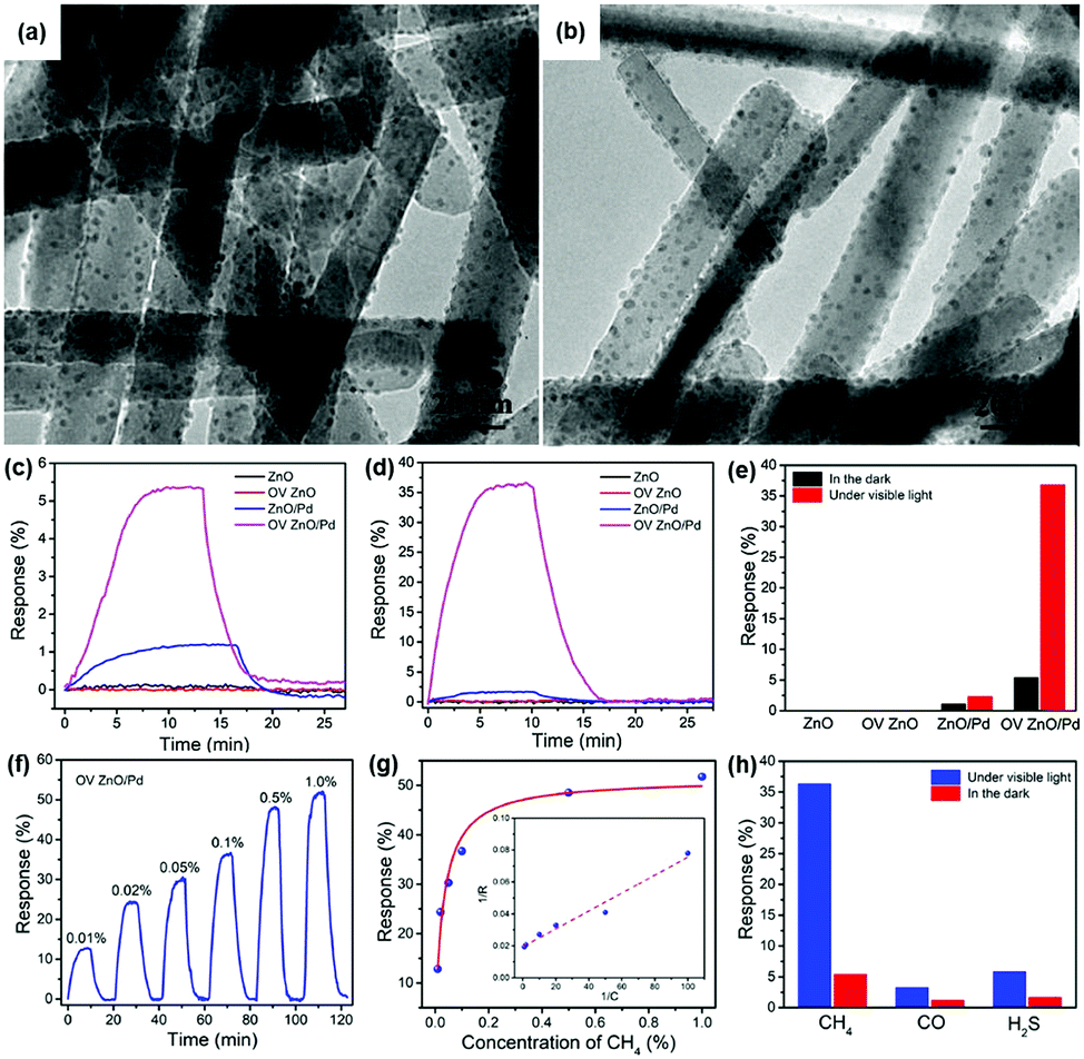 | ||
| Fig. 13 TEM images of the (a) ZnO/Pd and (b) OV ZnO/Pd samples. (c) Dynamic response curves of the sensors based on the ZnO, OV ZnO, ZnO/Pd and OV ZnO/Pd samples to 0.1% CH4 in the darkness and (d) under 590 nm light illumination (6 mW cm−2), and (e) the corresponding gas sensing responses. (f) Dynamic response curve and (g) fitted responses of the OV ZnO/Pd sensor to 0.01–1% CH4 under 590 nm light illumination (6 mW cm−2). (h) Selectivity of the OV ZnO/Pd sensor to 0.1% CH4 over CO and H2S under 590 nm light illumination (6 mW cm−2). Reproduced with permission from ref. 39. Copyright © 2020 Elsevier B.V. | ||
4.2 Nanostructures
The formation of nanostructures can be another good strategy to enhance light-activated gas sensing properties. Some of the previously reviewed works in this paper also adopted various nanostructures for better gas sensing properties, but most of them took advantage of increased surface area and provided no more detailed explanation beyond that.38,39,42,50,63 In fact, the differences in the nanostructural morphologies provide varying fractions of exposed polar facets, resulting in different light-activated gas sensing properties.J. Cui et al. synthesized ZnO nanofibers, nanoplates, and nanoflowers by simple electrospinning and hydrothermal methods.43 Compared to other metal oxides, ZnO has distinctive growth directions that make it facile to realize various ZnO nanostructures through simple control of growth conditions.125Fig. 14a–c show the SEM images of ZnO nanoplates, nanoflowers, and nanofibers, respectively. The ZnO nanoplates have a hexagonal morphology with 4 μm diameter and 400 nm thickness, and the ZnO nanoflowers exhibit 3D nanostructures with a diameter in the range of 4–5 μm, which are composed of numerous nanosheets with 80 nm thickness. The ZnO nanofibers have a diameter of 500–600 nm, and they are composed of tiny nanocrystallites, while the previous two morphologies (nanoplates and nanoflowers) have a relatively smooth surface. The fabricated gas sensors based on each ZnO nanostructure were exposed to different concentrations of HCHO under 365 nm UV light illumination at room temperature, as shown in Fig. 14d–f. Fig. 14g summarizes the gas responses of the gas sensors with each ZnO nanostructure toward HCHO. Among the three nanostructures, ZnO nanofibers exhibited the highest gas response, which was 6.7 times and 2.5 times higher than that of ZnO nanoplates and ZnO nanoflowers, respectively. These could be attributed to a higher specific area for ZnO nanofibers and polycrystalline structure with a large number of grain boundaries. The overall gas sensing mechanism follows that of conventional light-activated gas sensing. The photocatalytically adsorbed oxygen molecules that are loosely bound to the surface provide much more sensitive detection of target gas molecules. Since ZnO nanofibers in this study are composed of numerous nanocrystallites with an average size of 45 nm, Schottky barriers formed at each grain boundary after oxygen adsorption and its charge transfer contribute to the sensitive modulation upon adsorption and desorption of target gas molecules.126 However, ZnO nanoplates and nanoflowers have fewer grain boundaries to result in thinner depletion layers than ZnO nanofibers. In fact, three ZnO nanostructures have been prepared by different preparation methods from each other and that may have caused a significant influence on the light-activated gas sensing characteristics for each. Still, this study has revealed the importance of grain size and grain boundary density to light-activated gas sensing properties, providing important parameters for nanostructure designs.
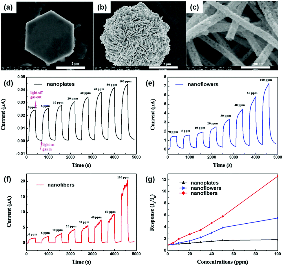 | ||
| Fig. 14 SEM images of (a) ZnO nanoplates, (b) ZnO nanoflowers, and (c) ZnO nanofibers. The current response cycles of (d) ZnO nanoplates, (e) ZnO nanoflowers and (f) ZnO nanofibers to different concentrations of formaldehyde and (g) the gas-sensing responses with a bias voltage of 10 V under 365 nm light irradiation at room temperature. Reproduced with permission from ref. 43. Copyright © 2016 Elsevier B. V. | ||
M. R. Alenezi et al. reported the UV light-activated gas sensing properties of three ZnO nanostructures (nanowires, nanodisks, and nanostars), which were all prepared by hydrothermal synthesis.44 Each nanostructure exhibits different ratios of exposed polar to nonpolar facets, and they can significantly affect light-activated gas sensing characteristics. Fig. 15a–c show the SEM images of ZnO nanowires, ZnO nanodisks, and ZnO nanostars, respectively. The photograph of the fabricated gas sensors based on ZnO nanostructures on flexible substrates is shown in Fig. 15d. ZnO nanowires exhibited 200 nm diameter and 8 μm length, and they have been formed through the growth direction of [0001], resulting in their nonpolar side surface with the {10![[1 with combining macron]](https://www.rsc.org/images/entities/char_0031_0304.gif) 0} orientation exposed.127,128 ZnO nanodisks have several tens of nanometer-scale thickness with high transparency, as shown in SEM images, and they have grown in a perpendicular direction to [0001]. Lastly, ZnO nanostars are composed of several nanowires with 150–200 nm diameter and expected to have similar crystallographic characteristics to ZnO nanowires. Fig. 15e summarizes the growth conditions of each ZnO nanostructure. According to the X-ray diffraction (XRD) analysis for each nanostructure, intensity ratios of the (0002) polar plane to the (100) nonpolar plane were calculated to be 0.36, 2.10, and 0.50 for ZnO nanowires, nanodisks, and nanostars, respectively. ZnO nanodisks exposed relatively more polar facets to air, while the other two morphologies exposed relatively nonpolar facets. The fabricated gas sensors based on ZnO nanowires, nanodisks, and nanostars were exposed to 200 ppm C2H5OH under different operating temperatures, and their results are summarized in Fig. 15f and g. The ZnO nanodisks exhibited the highest gas response at all operating temperatures over ZnO nanowires and nanostars. The optimal operating temperature exists since higher temperatures provide higher energy for surface activation, while excessively high operating temperatures accelerate the desorption kinetics of the sensing materials to yield lower gas responses.129 The UV light-activated gas sensing properties of the gas sensors at room temperature are summarized in Fig. 15h and i. The ZnO nanodisks exhibited the highest gas responses under all UV light intensities, corresponding to the thermally activated gas sensing results. As did for all metal oxide-based light-activated gas sensors, the photocatalytically adsorbed oxygen molecules play a critical role in the sensitive gas sensing characteristics of ZnO nanodisks under light activation. In addition to photocatalytic activation, ZnO nanodisks exhibited higher intensity ratios of the (0002) polar plane to the (100) nonpolar plane than other morphologies as mentioned before. The (0001) polar facet of ZnO nanodisks is terminated with Zn2+ ions in ZnO crystal lattices, and they are favorable active sites for oxygen adsorption. However, the {100} nonpolar planes for ZnO nanowires and nanostars have equivalent Zn and O atoms at the termination of the ZnO lattice, leading to less oxygen adsorption. Therefore, ZnO nanodisks could exhibit the highest chemisorption ability for the gas sensing reaction, resulting in the highest gas responses under UV light illumination.
0} orientation exposed.127,128 ZnO nanodisks have several tens of nanometer-scale thickness with high transparency, as shown in SEM images, and they have grown in a perpendicular direction to [0001]. Lastly, ZnO nanostars are composed of several nanowires with 150–200 nm diameter and expected to have similar crystallographic characteristics to ZnO nanowires. Fig. 15e summarizes the growth conditions of each ZnO nanostructure. According to the X-ray diffraction (XRD) analysis for each nanostructure, intensity ratios of the (0002) polar plane to the (100) nonpolar plane were calculated to be 0.36, 2.10, and 0.50 for ZnO nanowires, nanodisks, and nanostars, respectively. ZnO nanodisks exposed relatively more polar facets to air, while the other two morphologies exposed relatively nonpolar facets. The fabricated gas sensors based on ZnO nanowires, nanodisks, and nanostars were exposed to 200 ppm C2H5OH under different operating temperatures, and their results are summarized in Fig. 15f and g. The ZnO nanodisks exhibited the highest gas response at all operating temperatures over ZnO nanowires and nanostars. The optimal operating temperature exists since higher temperatures provide higher energy for surface activation, while excessively high operating temperatures accelerate the desorption kinetics of the sensing materials to yield lower gas responses.129 The UV light-activated gas sensing properties of the gas sensors at room temperature are summarized in Fig. 15h and i. The ZnO nanodisks exhibited the highest gas responses under all UV light intensities, corresponding to the thermally activated gas sensing results. As did for all metal oxide-based light-activated gas sensors, the photocatalytically adsorbed oxygen molecules play a critical role in the sensitive gas sensing characteristics of ZnO nanodisks under light activation. In addition to photocatalytic activation, ZnO nanodisks exhibited higher intensity ratios of the (0002) polar plane to the (100) nonpolar plane than other morphologies as mentioned before. The (0001) polar facet of ZnO nanodisks is terminated with Zn2+ ions in ZnO crystal lattices, and they are favorable active sites for oxygen adsorption. However, the {100} nonpolar planes for ZnO nanowires and nanostars have equivalent Zn and O atoms at the termination of the ZnO lattice, leading to less oxygen adsorption. Therefore, ZnO nanodisks could exhibit the highest chemisorption ability for the gas sensing reaction, resulting in the highest gas responses under UV light illumination.
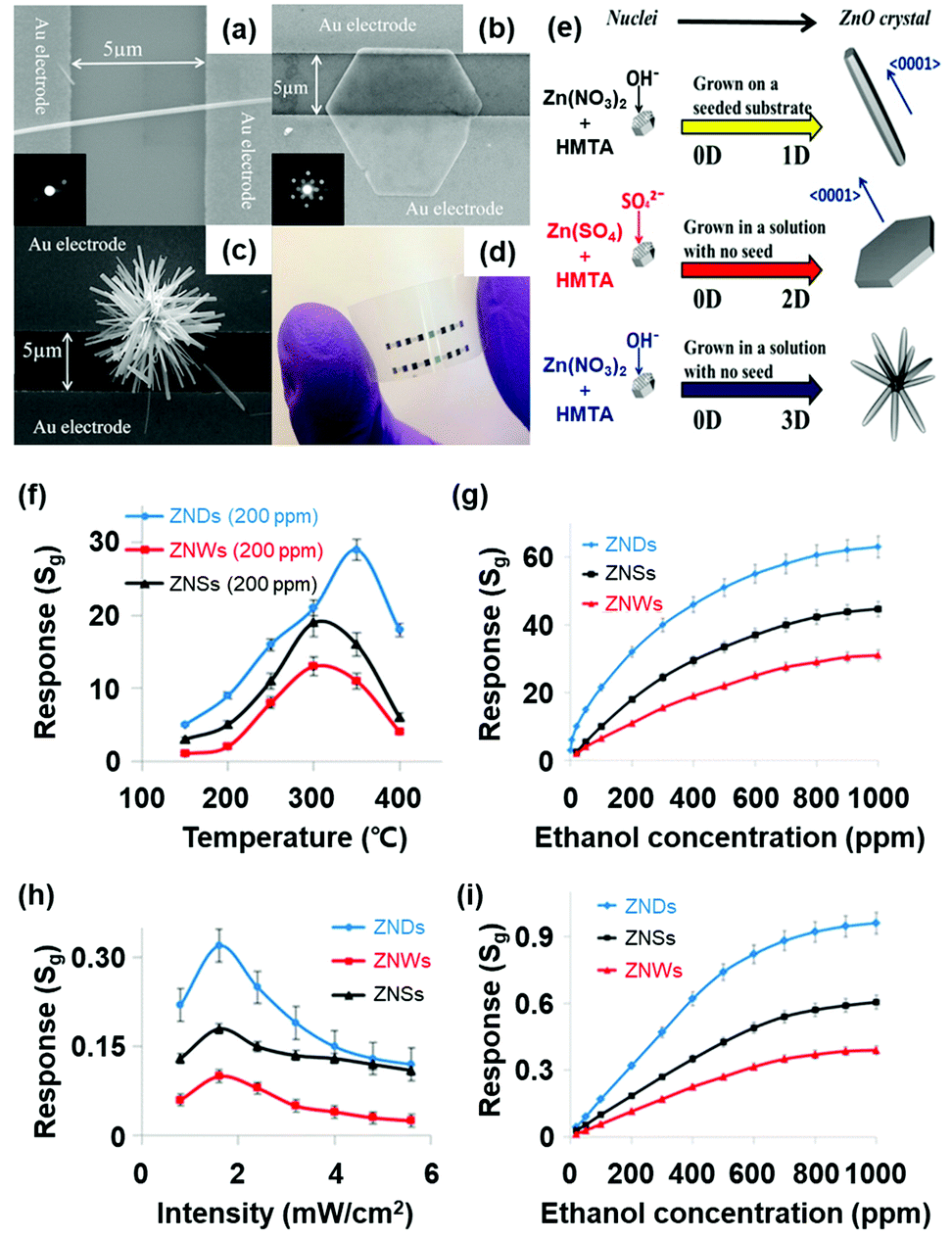 | ||
| Fig. 15 (a) SEM image of a ZnO nanowires (inset: SAED pattern), (b) ZnO nanodisks (inset: SAED pattern of ZNDs), and (c) ZnO nanostars. (d) Photograph of ZnO nanostructured sensors on a flexible substrate. (e) Schematic diagram of the growth process for each ZnO nanostructure. (f) Responses to 200 ppm C2H5OH at different temperatures. (g) Response vs time curves to different C2H5OH concentrations at 350 °C. (h) Responses to 200 ppm of C2H5OH at different light intensities. (i) Response vs time curves to different C2H5OH concentrations at 1.6 mW cm−2. Reproduced with permission from ref. 44. Copyright © 2013 American Chemical Society. | ||
4.3 Micro-LED integration
As reviewed, various materials including metal oxides, 2D materials, inorganic perovskites, metal sulfides, and organic semiconductors have been utilized to develop high-performance light-activated gas sensors. Certainly, the light-activation exhibited promising gas sensing characteristics and visualized their possibility and capabilities of replacing currently dominating thermally activated gas sensors in aspects of both performance and power consumption. However, the structure of the sensor devices should also be studied considering the practical application of light-activated gas sensors. Current thermally activated gas sensors have heater electrodes integrated under the gas sensing electrodes on a single substrate. However, current light-activated gas sensors utilize separate light sources that are not integrated on a single substrate, making them reluctant for practical applications. Therefore, further efforts on integration of light sources to gas sensor devices should be proceeded to get close to the real application of the light-activated gas sensors.130–132I. Cho, et al. reported monolithic micro-LEDs/metal oxide nanowire gas sensors that exhibit microwatt-level power consumption.45Fig. 16a and b show the schematic illustrations of the proposed monolithic gas sensors on micro-LEDs. The device has two contact pads for LED operation and the other two electrodes for gas sensor operation. The GaN-based micro-LEDs exhibit a peak emission wavelength of 390 nm, enough to activate metal oxides. The upper area of micro-LED was passivated via chemical vapor deposition of SiO2, and hydrothermally grown ZnO nanowires were located on the interdigitated electrodes on the top of the SiO2 passivation layer. Fig. 16c–e show the optical microscopic images of the devices with different widths of micro-LED (200, 100, and 30 μm, respectively). Fig. 16f shows the optical microscopic image of the device with a 30 μm LED width under operation. The SEM images of the synthesized ZnO nanowires on the fabricated device can be clearly seen in Fig. 16g. Then, the fabricated devices with different widths were exposed to 1 ppm NO2 gas with varying input powers to micro-LEDs, as shown in Fig. 16h and i. The base resistance of the device decreases as the input power to micro-LEDs increases, indicating a higher number of photogenerated charge carriers under a higher micro-LED power. The overall resistance for the device with 30 μm width is higher than that for the device with 200 μm width. This could be attributed to a limited conduction path through ZnO nanowires for the devices with a small width, since the gap between each electrode (5 μm) is consistent for all devices. The sensor responses were the highest for the micro-LEDs with the smallest width (30 μm), and the responses were not always the highest under the highest input power. These can be explained by the current spreading of micro-LEDs. With the increase in the width of micro-LEDs, the lateral series resistance increases and current spreading becomes inhomogeneous, leading to the possible less irradiating region to the gas sensing layers. These dead zones can be minimized by reducing the width of micro-LEDs, and this can support the highest gas responses for the devices with 30 μm-width micro-LEDs. The light-activated gas sensor responses are also highly dependent on the balance of surface absorbate density (O2 and NO2). Under the dark condition, only pre-adsorbed oxygen exists on the surface, while all the absorbates are totally desorbed under the high flux of illuminated light.133 Therefore, there should be an optimal balance between dark and high flux conditions, and which resulted in the optimal input power to micro-LEDs to yield the highest gas responses. Fig. 16j and k show the dynamic responses to 0.25–2 ppm NO2 and 60–250 ppb NO2, respectively. These data well support the stable and reliable operation of the monolithic micro-LEDs/metal oxide nanowire gas sensors over a wide concentration range of target gases.
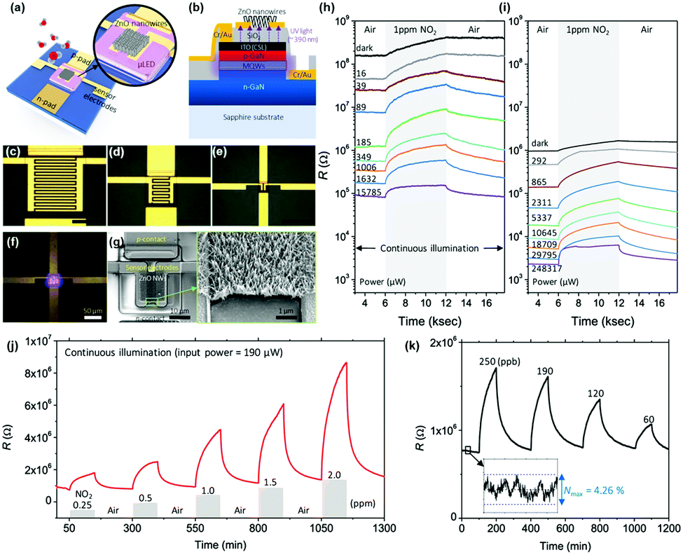 | ||
| Fig. 16 Schematic of the proposed monolithic photoactivated gas sensors on a microLED platform (μLP): (a) top view and (b) cross-sectional view. Optical microscopic images of fabricated LPs are as follows: (c–e) 200 × 200 (200-LP), 100 × 100 (100-LP), and 30 × 30 (30-μLP) μm2, respectively. Scale bars are 100 μm. (f) Optical microscopic image of a turned-on 30-μLP (forward bias = 5 V). (g) SEM images of synthesized zinc oxide (ZnO) nanowires on a prefabricated 30-μLP. Responses of monolithic photoactivated gas sensors on (h) 30-μLP and (i) 200-LP to 1 ppm NO2 gas under different input electrical powers. NO2 sensing performance of the photoactivated gas sensor on 30-μLP. Whole tests were conducted under an operating power of ∼190 μW: dynamic response to (j) 0.25–2 ppm and (k) 60–250 ppb NO2 gas. The inset graph shows the noise level of the measurement. Reproduced with permission from ref. 45. Copyright © 2020 American Chemical Society. | ||
5. Conclusion and perspective
In this review, the recent progress of light-activated gas sensors was summarized. Light-activated gas sensing has started with UV illumination on metal oxides, and the available light spectrum range has been expanded to the visible light range by utilization of low-bandgap materials such as 2D materials. While metal oxides and 2D materials have been two major candidate materials for light-activated gas sensing, inorganic perovskites, metal sulfides, and conductive polymers also exhibited their potential for future applications. Despite their promising gas sensing properties under light illumination at room temperature, the lack of selectivity toward reducing gases remained a challenge necessitating future research due to insufficient activation energy for their oxidation. The studies on the effects of nanostructures provided a deeper understanding of light activation depending on the exposed crystallographic orientations. In particular, the utilization of plasmonic nanoparticles and their localized surface plasmon resonance effects can dramatically enhance the light-activated gas sensing performance. The plasmonic nanoparticles can broaden the available light wavelength range, enhance gas sensing properties by hot electron generation, and take advantage of the catalytic effect and chemical sensitization of noble metal nanoparticles. Moreover, the integration with micro-LEDs suggested a possible device structure for the practical application of the light-activated gas sensors (Fig. 17). Collectively, proper and systematic design of light-activated gas sensors based on the following parameters can provide a promising perspective toward future gas sensor applications for IoE: (i) principles of material selection (bandgap, heterojunctions, or plasmonic nanoparticles), (ii) design of nanostructures, (iii) device structures and fabrication methods, and (iv) overall gas sensing mechanisms considering the relationship between light irradiation and gas sensing materials and the resulting gas sensing properties.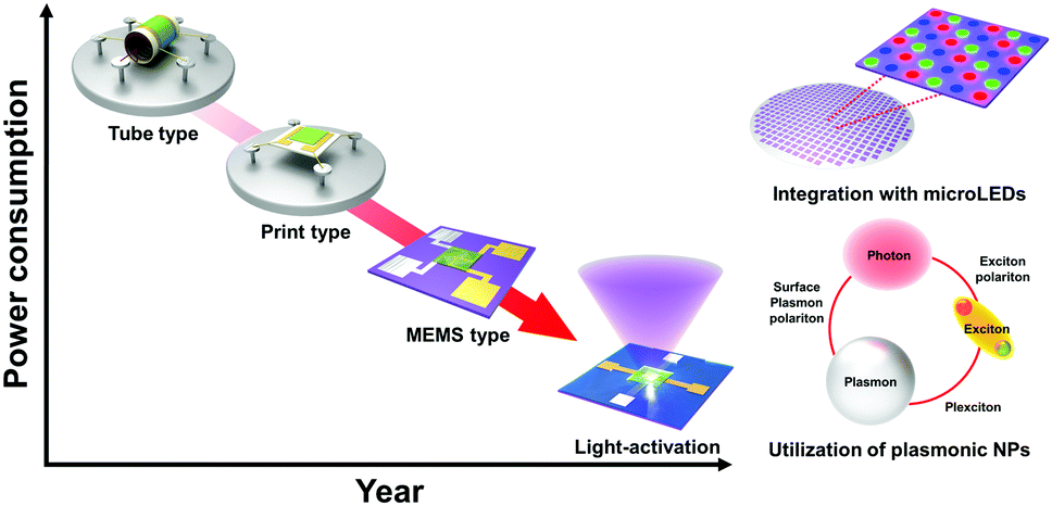 | ||
| Fig. 17 Schematic of the future perspectives of the light-activated gas sensors. | ||
Conflicts of interest
The authors declare that there are no conflicts of interest.Acknowledgements
This work was financially supported by Basic Science Research Program (2017R1A2B3009135), Nano·Material Technology Development Program (2016M3A7B4910), and Nuclear Energy R&D Program (2020M2D8A206983011) through the National Research Foundation of Korea funded by the Ministry of Science and ICT.References
- R. A. Potyrailo, Chem. Rev., 2016, 116, 11877–11923 CrossRef CAS.
- J. B. A. Gomes, J. J. P. C. Rodrigues, R. A. L. Rabelo, N. Kumar and S. Kozlov, J. Sens. Actuator Netw., 2019, 8, 57 CrossRef.
- D. Xie, D. Chen, S. Peng, Y. Yang, L. Xu and F. Wu, IEEE Electron Device Lett., 2019, 40, 1178–1181 CAS.
- H. Yuan, J. Tao, N. Li, A. Karmakar, C. Tang, H. Cai, S. J. Pennycook, N. Singh and D. Zhao, Angew. Chem., Int. Ed., 2019, 58, 14089–14094 CrossRef CAS.
- I. A. Buryakov, T. I. Buryakov and V. T. Matsayev, J. Anal. Chem., 2016, 71, 234–242 CrossRef CAS.
- A. Paliwal, A. Sharma, M. Tomar and V. Gupta, Sens. Actuators, B, 2017, 250, 679–685 CrossRef CAS.
- B. Sharma and J.-S. Kim, Sci. Rep., 2018, 8, 5902 CrossRef.
- X. Duan, S. Kamin and N. Liu, Nat. Commun., 2017, 8, 14606 CrossRef CAS.
- S. Mulmi and V. Thangadurai, J. Electrochem. Soc., 2020, 167, 037567 CrossRef CAS.
- Z. Duan, Y. Zhang, Y. Tong, H. Zou, J. Peng and X. Zheng, J. Electron. Mater., 2017, 46, 6895–6900 CrossRef CAS.
- S. Y. Park, Y. Kim, T. Kim, T. H. Eom, S. Y. Kim and H. W. Jang, InfoMat, 2019, 1, 289–316 CrossRef CAS.
- H. Tai, Z. Duan, Y. Wang, S. Wang and Y. Jiang, ACS Appl. Mater. Interfaces, 2020, 12, 31037–31053 CrossRef CAS.
- H. Tai, S. Wang, Z. Duan and Y. Jiang, Sens. Actuators, B, 2020, 318, 128104 CrossRef CAS.
- J. M. Suh, Y.-S. Shim, D. H. Kim, W. Sohn, Y. Jung, S. Y. Lee, S. Choi, Y. H. Kim, J.-M. Jeon, K. Hong, K. C. Kwon, S. Y. Park, C. Kim, J.-H. Lee, C.-Y. Kang and H. W. Jang, Adv. Mater. Technol., 2017, 2, 1600259 CrossRef.
- J. M. Suh, W. Sohn, Y.-S. Shim, J.-S. Choi, Y. G. Song, T. L. Kim, J.-M. Jeon, K. C. Kwon, K. S. Choi, C.-Y. Kang, H.-G. Byun and H. W. Jang, ACS Appl. Mater. Interfaces, 2017, 10, 1050–1058 CrossRef.
- Y. G. Song, J. Y. Park, J. M. Suh, Y.-S. Shim, S. Y. Yi, H. W. Jang, S. Kim, J. M. Yuk, B.-K. Ju and C.-Y. Kang, Chem. Mater., 2018, 31, 207–215 CrossRef.
- S. Y. Yi, Y. G. Song, J. Y. Park, J. M. Suh, G. S. Kim, Y.-S. Shim, J. M. Yuk, S. Kim, H. W. Jang, B.-K. Ju and C.-Y. Kang, ACS Appl. Mater. Interfaces, 2019, 11, 7529–7538 CrossRef CAS.
- D. H. Kim, T. H. Kim, W. Sohn, J. M. Suh, Y.-S. Shim, K. C. Kwon, K. Hong, S. Choi, H.-G. Byun, J.-H. Lee and H. W. Jang, Sens. Actuators, B, 2018, 274, 587–594 CrossRef CAS.
- Y.-S. Shim, B. Jang, J. M. Suh, M. S. Noh, S. Kim, S. D. Han, Y. G. Song, C.-Y. Kang, H. W. Jang and W. Lee, Sens. Actuators, B, 2018, 255, 1841–1848 CrossRef CAS.
- Y. G. Song, Y.-S. Shim, J. M. Suh, M.-S. Noh, G. S. Kim, K. S. Choi, B. Jeong, S. Kim, H. W. Jang, B.-K. Ju and C.-Y. Kang, Small, 2019, 15, 1902065 CrossRef.
- H. Tai, Z. Duan, Z. He, X. Li, J. Xu, B. Liu and Y. Jiang, Sens. Actuators, B, 2019, 298, 126874 CrossRef CAS.
- Q. Zhao, Z. Duan, Z. Yuan, X. Li, S. Wang, B. Liu, Y. Zhang, Y. Jiang and H. Tai, Chin. Chem. Lett., 2020, 31, 2045–2049 CrossRef CAS.
- Y.-S. Shim, K. C. Kwon, J. M. Suh, K. S. Choi, Y. G. Song, W. Sohn, S. Choi, K. Hong, J.-M. Jeon, S.-P. Hong, S. Kim, S. Y. Kim, C.-Y. Kang and H. W. Jang, ACS Appl. Mater. Interfaces, 2018, 10, 31594–31602 CrossRef CAS.
- K. C. Kwon, J. M. Suh, T. H. Lee, K. S. Choi, K. Hong, Y. G. Song, Y.-S. Shim, M. Shokouhimehr, C.-Y. Kang, S. Y. Kim and H. W. Jang, ACS Sens., 2019, 4, 678–686 CrossRef CAS.
- Y. H. Kim, Y. S. Choi, S. Y. Park, T. Kim, S.-P. Hong, T. H. Lee, C. W. Moon, J.-H. Lee, D. Lee, B. H. Hong and H. W. Jang, Nanoscale, 2019, 11, 2966–2973 RSC.
- Y. H. Kim, K. C. Kwon, S. Kang, C. Kim, T. H. Kim, S.-P. Hong, S. Y. Park, J. M. Suh, M.-J. Choi, S. Han and H. W. Jang, ACS Sens., 2019, 4, 2395–2402 CrossRef CAS.
- J. M. Suh, Y.-S. Shim, K. C. Kwon, J.-M. Jeon, T. H. Lee, M. Shokouhimehr and H. W. Jang, Electron. Mater. Lett., 2019, 15, 368–376 CrossRef CAS.
- S. Y. Park, Y. H. Kim, S. Y. Lee, W. Sohn, J. E. Lee, Y.-S. Shim, K. C. Kwon, K. S. Choi, H. J. Yoo, J. M. Suh, M. Ko, J.-H. Lee, M. J. Lee, S. Y. Kim, M. H. Lee and H. W. Jang, J. Mater. Chem. A, 2018, 6, 5016–5024 RSC.
- W. Zheng, Y. Xu, L. Zheng, C. Yang, N. Pinna, X. Liu and J. Zhang, Adv. Funct. Mater., 2020, 30, 2000435 CrossRef CAS.
- B. Han, Z. Duan, J. Xu, Y. Zhu, Q. Xu, H. Wang, H. Tai, J. Weng and Y. Zhao, Adv. Funct. Mater., 2020, 30, 2002232 CrossRef CAS.
- Z. Ma, P. Chen, W. Cheng, K. Yan, L. Pan, Y. Shi and G. Yu, Nano Lett., 2018, 18, 4570–4575 CrossRef CAS.
- Y. Jiang, N. Tang, C. Zhou, Z. Han, H. Qu and X. Duan, Nanoscale, 2018, 10, 20578–20586 RSC.
- C. H. A. Esteves, B. A. Iglesias, T. Ogawa, K. Araki, L. Hoehne and J. Gruber, ACS Omega, 2018, 3, 6476–6482 CrossRef CAS.
- N. Barsan and U. Weimar, J. Electroceram., 2001, 7, 143–167 CrossRef CAS.
- R. Prajesh, N. Jain and A. Agarwal, Microsyst. Technol., 2016, 22, 2185–2192 CrossRef CAS.
- F. Xu and H.-P. Ho, Micromachines, 2017, 8, 333 CrossRef.
- E. Espid and F. Taghipour, Crit. Rev. Solid State Mater. Sci., 2017, 42, 146–432 Search PubMed.
- F. Xu, H.-F. Lv, S.-Y. Wu and H.-P. Ho, Sens. Actuators, B, 2018, 259, 709–716 CrossRef CAS.
- R. Chen, J. Wang, S. Luo, L. Xiang, W. Li and D. Xie, Appl. Catal., B, 2020, 264, 118554 CrossRef CAS.
- H. Chen, M. Zhang, R. Bo, C. Barugkin, J. Zheng, Q. Ma, S. Huang, A. W. Y. Ho-Baillie, K. R. Catchpole and A. Tricoli, Small, 2018, 14, 1702571 CrossRef.
- H. Chen, M. Zhang, X. Fu, Z. Fusco, R. Bo, B. Xing, H. T. Nguyen, C. Barugkin, J. Zheng, C. F. J. Lau, S. Huang, A. W. Y. Ho-Baillie, K. R. Catchpole and A. Tricoli, Phys. Chem. Chem. Phys., 2019, 21, 24187–24193 RSC.
- H.-Y. Li, J.-W. Yoon, C.-S. Lee, K. Lim, J.-W. Yoon and J.-H. Lee, Sens. Actuators, B, 2018, 255, 2963–2970 CrossRef CAS.
- J. Cui, L. Shi, T. Xie, D. Wang and Y. Lin, Sens. Actuators, B, 2016, 227, 220–226 CrossRef CAS.
- M. R. Alenezi, A. S. Alshammari, K. D. G. I. Jayawardena, M. J. Beliatis, S. J. Henley and S. R. P. Silva, J. Phys. Chem. C, 2013, 117, 17850–17858 CrossRef CAS.
- I. Cho, Y. C. Sim, M. Cho, Y.-H. Cho and I. Park, ACS Sens., 2020, 5, 563–570 CrossRef CAS.
- D. A. Melnick, J. Chem. Phys., 1957, 26, 1136 CrossRef CAS.
- J. T. Cheung, US Pat., US005448906A, 1995.
- H.-J. Kim and J.-H. Lee, Sens. Actuators, B, 2014, 192, 607–627 CrossRef CAS.
- N. Yamazoe, G. Sakai and K. Shimanoe, Catal. Surv. Asia, 2003, 7, 63–75 CrossRef CAS.
- B. Liu, Y. Luo, K. Li, H. Wang, L. Gao and G. Duan, Adv. Mater. Interfaces, 2019, 6, 1900376 CrossRef.
- L. Liu, X. Li, P. K. Dutta and J. Wang, Sens. Actuators, B, 2013, 185, 1–9 CrossRef CAS.
- R. Kumar, N. Goel and M. Kumar, ACS Sens., 2017, 2, 1744–1752 CrossRef CAS.
- X. Tian, X. Yang, F. Yang and T. Qi, Colloids Surf., A, 2019, 578, 123621 CrossRef CAS.
- D. Klaus, D. Klawinski, S. Amrehn, M. Tiemann and T. Wagner, Sens. Actuators, B, 2015, 217, 181–185 CrossRef CAS.
- M. Kumar, R. Kumar, S. Rajamani, S. Ranwa, M. Fanetti, M. Valant and M. Kumar, Nanotechnology, 2017, 28, 365502 CrossRef.
- H. Wang, L. Zhou, Y. Liu, F. Liu, X. Liang, F. Liu, Y. Gao, X. Yan and G. Lu, Sens. Actuators, B, 2020, 305, 127498 CrossRef CAS.
- S. Zhang, L. Zhao, B. Huang and X. Li, Sens. Actuators, B, 2020, 319, 128264 CrossRef CAS.
- N. D. Chinh, C. Kim and D. Kim, J. Alloys Compd., 2019, 778, 247–255 CrossRef CAS.
- Y. Chen, X. Li, X. Li, J. Wang and Z. Tang, Sens. Actuators, B, 2016, 232, 158–164 CrossRef CAS.
- G. Maduraiveeran, M. Sasidharan and W. Jin, Prog. Mater. Sci., 2019, 106, 100574 CrossRef CAS.
- G. Ingrosso, Microchem. J., 2002, 73, 221 CrossRef CAS.
- K. R. Marllires, D. Wang, V. V. Tipparaju and N. Tao, IEEE Sens. J., 2019, 19, 8252–8261 Search PubMed.
- B. Wang, W. Huang, L. Chi, M. Al-Hashimi, T. J. Marks and A. Facchetti, Chem. Rev., 2018, 118, 5690–5754 CrossRef CAS.
- X.-X. Wang, H.-Y. Li and X. Gio, J. Mater. Chem. A, 2020, 8, 14482–14490 RSC.
- E. Espid, A. S. Noce and F. Taghipour, J. Photochem. Photobiol., A, 2019, 374, 95–105 CrossRef CAS.
- A. Ilin, M. Martyshov, E. Forsh, P. Forsh, M. Rumyantseva, A. Abakumov, A. Gaskov and P. Kashkarov, Sens. Actuators, B, 2016, 231, 491–496 CrossRef CAS.
- A. S. Chizkov, M. N. Rumyantseva, R. B. Vasiliev, D. G. Filatova, K. A. Drozdov, I. V. Krylov, A. V. Marchevsky, O. M. Karakulina, A. M. Abakumov and A. M. Gaskov, Thin Solid Films, 2016, 618, 253–262 CrossRef.
- N. D. Chinh, N. D. Quang, H. Lee, T. T. Hien, N. M. Hieu, D. Kim, C. Kim and D. Kim, Sci. Rep., 2016, 6, 35066 CrossRef CAS.
- R. Jaisutti, J. Kim, S. K. Park and Y.-H. Kim, ACS Appl. Mater. Interfaces, 2016, 8, 20192–20199 CrossRef CAS.
- S. C. Chang, J. Vac. Sci. Technol., 1980, 17, 366–369 CrossRef CAS.
- Y. Nakamura, Y. Ishikawa, Y. Morita, H. Takagi and S. Fujitsu, Sens. Actuators, B, 2013, 187, 578–585 CrossRef CAS.
- S. Park, S. An, Y. Mun and C. Lee, ACS Appl. Mater. Interfaces, 2013, 5, 4285–4292 CrossRef CAS.
- G. Lu, J. Xu, J. Sun, Y. Yu, Y. Zhang and F. Liu, Sens. Actuators, B, 2012, 162, 82–88 CrossRef CAS.
- E. Wongrat, N. Chanlek, C. Chueaiarrom, B. Samransuksamer, N. Hongsith and S. Choopun, Sens. Actuators, A, 2016, 251, 188–197 CrossRef CAS.
- F. H. Saboor, T. Ueda, K. Kamada, T. Hyodo, Y. Mortazavi, A. A. Khodadadi and Y. Shimizu, Sens. Actuators, B, 2016, 223, 429–439 CrossRef CAS.
- A. Berholts, T. Kahro, A. Floren, H. Alles and R. Jaaniso, Appl. Phys. Lett., 2014, 105, 163111 CrossRef.
- X. Geng, C. Zhang, M.-G. Olivier and M. Debliquy, Proceedings, 2017, 1, 411 CrossRef.
- K. T. Alali, J. Liu, J. Yu, D. Moharram, R. Chen, H. Zhang, Q. Liu, M. Zhang and J. Wang, J. Alloys Compd., 2020, 832, 154999 CrossRef CAS.
- Q. A. Drmosh, A. H. Hendi, M. K. Hossain, Z. H. Yamani, R. A. Moqbel, A. Hezam and M. A. Gondal, Sens. Actuators, B, 2019, 290, 666–675 CrossRef CAS.
- V. Paolucci, S. M. Emamjomeh, L. Ottaviano and C. Cantalini, Sensors, 2019, 19, 2617 CrossRef CAS.
- M. Reddeppa, B.-G. Park, G. Murali, S. H. Choi, N. D. Chinh, D. Kim, W. Yang and M.-D. Kim, Sens. Actuators, B, 2020, 308, 127700 CrossRef CAS.
- W. Zhang, Z. Huang, W. Zhang and Y. Li, Nano Res., 2014, 7, 1731–1737 CrossRef CAS.
- G. Chen, T. M. Paronyan, E. M. Pigos and A. R. Harutyunyan, Sci. Rep., 2012, 2, 343 CrossRef.
- D. Gu, X. Li, H. Wang, M. Li, Y. Xi, Y. Chen, J. Wang, M. N. Rumyntseva and A. M. Gaskov, Sens. Actuators, B, 2018, 256, 992–1000 CrossRef CAS.
- D. Gu, X. Wang, W. Liu, X. Li, S. Lin, J. Wang, M. N. Rumyantseva, A. M. Gaskov and S. A. Akbar, Sens. Actuators, B, 2020, 305, 127455 CrossRef CAS.
- S. R. Damkale, S. S. Arbuj, G. G. Umarji, R. P. Panmand, S. K. Khore, R. S. Sonawane, S. B. Rane and B. B. Kale, Sustainable Energy Fuels, 2019, 3, 3406–3414 RSC.
- E. Huang, X. Yao, W. Wang, G. Wu, N. Guan and L. Li, ChemPhotoChem, 2017, 1, 60–69 CrossRef CAS.
- Y. Huang, W. Jiao, Z. Chu, G. Ding, M. Yan, X. Zhong and R. Wang, J. Mater. Chem. C, 2019, 7, 8616 RSC.
- D. J. Late, Y.-K. Huang, B. Liu, J. Acharya, S. N. Shirodkar, J. Luo, A. Yan, D. Charles, U. V. Waghmare and V. P. Dravid, ACS Nano, 2013, 7, 4879–4891 CrossRef CAS.
- E. Comini, A. Cristalli, G. Faglia and G. Sberveglieri, Sens. Actuators, B, 2000, 65, 260–263 CrossRef CAS.
- K. Anothainart, M. Burgmair, A. Karthigeyan, M. Zimmer and I. Eisele, Sens. Actuators, B, 2003, 93, 580–584 CrossRef CAS.
- J. Wang, H. Deng, X. Li, C. Yang and Y. Xia, Sens. Actuators, B, 2020, 304, 127317 CrossRef CAS.
- H. Chen, Y. Chen, H. Zhang, D. W. Zhang, P. Zhou and J. Huang, Adv. Funct. Mater., 2018, 28, 1801035 CrossRef.
- X. Geng, C. Zhang and M. Debliquy, Ceram. Int., 2016, 42, 4845–4852 CrossRef CAS.
- S. Park, G.-J. Sun, H. Kheel, T. Ko, H. W. Kim and C. Lee, Appl. Phys. A: Mater. Sci. Process., 2016, 122, 504 CrossRef.
- Z. Yang, L. Guo, B. Zu, Y. Guo, T. Xu and X. Dou, Adv. Opt. Mater., 2014, 2, 738–745 CrossRef CAS.
- S. Park, S. An, H. Ko, S. Lee and C. Lee, Sens. Actuators, B, 2013, 188, 1270–1276 CrossRef CAS.
- A. S. Chizhov, M. N. Rumyantseva, R. B. Vasiliev, D. G. Filatova, K. A. Drozdov, I. V. Krylov, A. M. Abakumov and A. M. Gaskov, Sens. Actuators, B, 2014, 205, 305–312 CrossRef CAS.
- S. Park, S. An, Y. Mun and C. Lee, Curr. Appl. Phys., 2014, 14, 557–562 Search PubMed.
- A. S. Chizhov, M. N. Rumyantseva, R. B. Vasiliev, D. G. Filatova, K. A. Drozdov, I. V. Krylov, A. V. Marchevsky, O. M. Karakulina, A. M. Abakumov and A. M. Gaskov, Thin Solid Films, 2016, 253–262 CrossRef CAS.
- G. Magna, A. Catini, R. Kumar, M. Palmacci, E. Martinelli, R. Paolesse and C. D. Natale, Sensors, 2017, 17, 747 CrossRef.
- S. Nasirian, Appl. Surf. Sci., 2020, 502, 144302 CrossRef CAS.
- M. Reddeppa, T. Chandrakalavathi, B.-G. Park, G. Murali, R. Siranjeevi, G. Nagaraju, J. S. Yu, R. Jayalakshmi, S.-G. Kim and M.-D. Kim, Sens. Actuators, B, 2020, 307, 127649 CrossRef.
- G. Giorgi, J.-I. Fujisawa, H. Segawa and K. Yamashita, J. Phys. Chem. C, 2014, 118, 12176 CrossRef CAS.
- Y. Zhuang, W. Yuan, L. Qian, S. Chen and G. Shi, Phys. Chem. Chem. Phys., 2017, 19, 12876 RSC.
- M. Zhang, J. S. Yun, Q. Ma, J. Zheng, C. F. J. Lau, X. Deng, J. Kim, D. Kim, J. Seidel, M. A. Green, S. Huang and A. W. Y. Ho-Baillie, ACS Energy Lett., 2017, 2, 438–444 CrossRef CAS.
- J. K. Nam, D. H. Chun, R. J. K. Rhee, J. H. Lee and J. H. Park, Adv. Sci., 2018, 5, 1800509 CrossRef.
- S. Sergeyev, W. Pisula and Y. H. Geerts, Chem. Soc. Rev., 2007, 36, 1902–1929 RSC.
- J. E. Anthony, A. Facchetti, M. Heeney, S. R. Marder and X. W. Zhan, Adv. Mater., 2010, 22, 3876–3892 CrossRef CAS.
- M. El Gemayel, M. Treier, C. Musumeci, C. Li, K. Müllen and P. Samorì, J. Am. Chem. Soc., 2012, 134, 2429–2433 CrossRef.
- Y. Li, H. Jin, G. Sun, B. Zhang, N. Luo, H. Bala, J. Cao, Z. Zhang and Y. Wang, Phys. E, 2019, 106, 40–44 CrossRef CAS.
- E. Espid, B. Adeli and F. Taghipour, J. Electrochem. Soc., 2019, 166, H3223–H3230 CrossRef CAS.
- T. Dilova, G. Atanasova, A. O. Dikovska and N. N. Nedyalkov, Appl. Surf. Sci., 2020, 505, 144625 CrossRef CAS.
- C. Chen, Q. Zhang, G. Xie, M. Yao, H. Pan, H. Du, H. Tai, X. Du and Y. Su, Mater. Res. Express, 2020, 7, 015924 CrossRef CAS.
- J. Wang, S. Fan, Y. Xia, C. Yang and S. Komarneni, J. Hazard. Mater., 2020, 381, 120919 CrossRef CAS.
- Y. Yao, F. Ji, M. Yin, X. Ren, Q. Ma, J. Yan and S. F. Liu, ACS Appl. Mater. Interfaces, 2016, 8, 18165–18172 CrossRef CAS.
- Q. Zhang, G. Xie, M. Xu, Y. Su, H. Tai, H. Du and Y. Jiang, Sens. Actuators, B, 2018, 259, 269–281 CrossRef CAS.
- Y. Zhou, C. Zou, X. Lin and Y. Guo, Appl. Phys. Lett., 2018, 113, 082103 CrossRef.
- Y. Yao, M. Yin, J. Yan, D. Yang and S. Liu, Sens. Actuators, B, 2017, 251, 583–589 CrossRef CAS.
- Y. Sun, Y. Sun, T. Zhang, G. Chen, F. Zhang, D. Liu, W. Cai, Y. Li, X. Yang and C. Li, Nanoscale, 2016, 8, 10774–10782 RSC.
- K. Liu, Y. Bi, S. Qu, F. Tan, D. Chi, S. Lu, Y. Li, Y. Kou and Z. Wang, Nanoscale, 2014, 6, 6180–6186 RSC.
- S. K. Cushing, J. Li, F. Meng, T. R. Senty, S. Suri, M. Zhi, M. Li, A. D. Bristow and N. Wu, J. Am. Chem. Soc., 2012, 134, 15033–15041 CrossRef CAS.
- S. J. Han, S. K. Kim, A. Hwang, S. Kim, D.-Y. Hong, G. Kwak, K.-W. Jun and Y. T. Kim, Appl. Catal., B, 2019, 241, 305–318 CrossRef CAS.
- D. Wu, K. Deng, B. Hu, Q. Lu, G. Liu and X. Hong, ChemCatChem, 2019, 11, 1598–1601 CrossRef CAS.
- Z. L. Wang, J. Phys.: Condens. Matter, 2004, 16, R829–R858 CrossRef CAS.
- M. E. Franke, T. J. Koplin and U. Simon, Small, 2005, 2, 36–50 CrossRef.
- L. E. Greene, B. D. Yuhas, M. Law, D. Zitoun and P. Yang, Inorg. Chem., 2006, 45, 7535–7543 CrossRef CAS.
- Z. L. Wang, Mater. Sci. Eng., 2009, 64, 33–71 CrossRef.
- J. Herran, O. Fernandez-Gonzalez, I. Castro-Hurtado, T. Romero, G. G. Mandayo and E. Castano, Sens. Actuators, B, 2010, 149, 368–372 CrossRef CAS.
- C.-L. Hsu, L.-F. Chang and T.-J. Hseuh, Sens. Actuators, B, 2017, 249, 265–277 CrossRef CAS.
- O. Casals, N. Markiewicz, C. Fabrega, I. Gracia, C. Cane, H. S. Wasisto, A. Waag and J. D. Prades, ACS Sens., 2019, 4, 822–826 CrossRef CAS.
- N. Markiewicz, O. Casals, C. Fabrega, H. S. Wasisto, A. Waag and J. D. Prades, Proceedings, 2018, 2(13), 971 CrossRef.
- J. D. Prades, R. Jimenez-Diaz, M. Manzanares, F. Hernandez-Ramirez, A. Cirera, A. Romano-Rodriguez, S. Mathur and J. R. Morante, Phys. Chem. Chem. Phys., 2009, 11, 10881–10889 RSC.
Footnote |
| † These authors contributed equally to this work. |
| This journal is © The Royal Society of Chemistry 2021 |