
 Open Access Article
 This Open Access Article is licensed under a
 Creative Commons Attribution 3.0 Unported Licence
Metal halide perovskite nanocrystals: application in high-performance photodetectors
Dan
Liu
,
Yuxiao
Guo
,
Meidan
Que
 ,
Xingtian
Yin
*,
Jie
Liu
,
Haixia
Xie
,
Cong
Zhang
and
Wenxiu
Que
*
,
Xingtian
Yin
*,
Jie
Liu
,
Haixia
Xie
,
Cong
Zhang
and
Wenxiu
Que
*
Electronic Materials Research Laboratory, Key Laboratory of the Ministry of Education & International Center for Dielectric Research, Shaanxi Engineering Research Center of Advanced Energy Materials and Devices, School of Electronic Science and Engineering, Xi’an Jiaotong University, Xi'an 710049, Shaanxi, P. R. China. E-mail: xt_yin@mail.xjtu.edu.cn; wxque@mail.xjtu.edu.cn
First published on 16th December 2020
Abstract
Recently, perovskite nanocrystals (NCs) have become highly promising materials due to their unique optical and electrical properties such as high absorption coefficient, high photoluminescence quantum yield, and long exciton diffusion length. It is well known that the band gap of perovskite nanocrystals can be tuned by composition engineering, ranging from the ultraviolet to near-infrared regions. Moreover, thanks to the solution-processing feature, perovskite NCs have become much popular for various photodetectors. Hence, in this review, we carefully introduce the developmental progress of perovskite NCs and photodetectors, including the aspects of synthetic procedures, device architectures, working mechanism, and optimization procedures. Besides, great achievements and challenges, in terms of the high photosensitivity and detectivity, are also discussed for perovskite NC-based photodetectors. Finally, the application perspective of next generation photodetectors is prospected, which provides a reference for the related study.
1. Introduction
The environmental perception of humans has a profound impact in understanding the natural world as well as the production and life. Faced with a wide range of light wavelength (10–106 nm), it is obvious that the narrow visible light range (400–760 nm) restricts the human society. The advent of photodetectors, which convert incident light signals into processable electrical signals, is an inevitable choice for social development. Therefore, the detection from the ultraviolet visible to the infrared (UV-visible-IR) region has important applications in many fields, such as optical communication, industrial process monitoring, Lidar imaging, and night vision.1,2 At this stage, inorganic semiconductor material systems, including Si, II–VI and III–V compounds, have been suitably applied in the field of commercial photodetectors1–3 However, at the initial stage of photodetectors, Si, GaN, and other material systems are significantly dependent on chemical vapor deposition and photolithography. The high cost and low yield caused by the harsh high vacuum preparation environment and low quantum efficiency of chemical vapor deposition have become a problem that people urgently need to solve. With the wide application of flexible devices, such as wearable electronic devices and the need for diverse markets, the compatibility of inorganic materials with flexible substrates has become a huge challenge. In addition, from the range of spectral response, the inherent wide direct band gap of II–VI semiconductor materials limits the detection of the infrared spectrum; thus, eliminating the “visible area” blind spot is a problem that has to be solved.In 2009, Kojima et al. used perovskite as the photosensitive layer in solar cells for the first time and achieved an efficiency of 3.8%, which opens the door for the photovoltaic applications of metal halide perovskites.4 The emerging halide perovskite has become the object of pursuit for researchers due to its excellent photophysical properties. The perovskite material has a high absorption coefficient and the band gap tunability from UV-visible-IR can be achieved by adjusting the inherent composition. The high carrier mobility and long diffusion length also contributes to the efficient transport and collection of carriers. Besides, low-temperature crystallinity and the solution process are the foundation for the construction of flexible multifunctional devices with composite structures.5–9 From the time perovskite materials have entered the field of optoelectronic devices, three-dimensional (3D) halide perovskites have climbed to the top performance in just a few years, reaching a power conversion efficiency of 25.2% for photovoltaic devices.10 Although the performance of the 3D perovskite is commendable, its shortcomings have become more obvious. This kind of polycrystalline 3D material will inevitably produce the problem of grain boundary defects, resulting in a composite center, photocurrent hysteresis effect, and stability problems, which makes the performance improvement process encounter bottlenecks. In contrast, the high crystallinity of perovskite nanocrystals (NCs) naturally forms single crystals with fewer defects. The large surface area-to-volume ratio and quantum confinement effect brought by the nanometer scale can easily realize energy band engineering and customize the optoelectronic devices with special functions according to the requirements. In addition, in the application of flexible devices, the mechanical flexibility of perovskite NCs is better than that of the 3D perovskite. It can be seen that there will be better development in the large-scale industrialization in the future. Ramasamy et al. reported for the first time a photodetector based on CsPbI3 QDs, which has a good on/off photocurrent ratio of 105 at 405 nm.11 In recent years, it has ushered in vigorous development, with various forms of perovskite photodetectors emerging endlessly. The reported best light responsivity (R) exceeds 109 A W−1 and the response time is as low as 1 ns, which can be compared with conventional semiconductor photosensitive materials and commercial Si-based optoelectronic devices. It shows that the perovskite NC photodetector has certain market competitiveness in terms of the performance.
Currently, photodetectors with different structures and various working mechanisms have been developed based on metal halide perovskites NCs (for example, photoconductors, phototransistors, and photodiodes). A wide variety of devices also means that each has its own merits. For example, the amplification function of the transistors can achieve higher photocurrent gain. Combined with other functional materials (such as graphene, two-dimensional (2D) layer semiconductors, and organic semiconductors), it can be advantageous in weak light. For diodes with smaller electrode spacing, fast response speed and lower dark current are their advantages This article reviews the perovskite NCs photodetectors with different structures, including the combinations of various materials in different spectral ranges. The synthetic methods, post-processing methods, and the stability of the materials for NCs system are introduced comprehensively and systematically. In addition, based on the solution process of NCs, we also briefly introduce the liquid-phase film forming technology to promote this low-cost and efficient processing method. Here, we review the development history of perovskite NCs optoelectronic devices not only to introduce how optoelectronic devices are developed, but also to extensively collect various ingenious designs that promote the development of optoelectronic devices and provide inspiration for future optoelectronic devices. Finally, according to the current status of the perovskite NCs photodetector, the challenges and development prospects that may be encountered in the future are put forward to provide references for related research and development in the future.
2. Characteristics of ABX3 NCs
2.1 Microstructure of the ABX3 perovskite material
For morphological analysis, perovskite NCs are the same as 3D bulk halide perovskites. Their structure consists of the corner-sharing BX6 octahedral framework and A cation located in the octahedral cavity. The general chemical formula of halide perovskites can be expressed as ABX3, where A is a monovalent cation, usually composed of methylammonium (MA+, CH3NH3+), ethylammonium (FA+, CH(NH2)2+), or inorganic cesium (Cs+), B is a divalent metal cation, usually composed of lead (Pb2+) or tin (Sn2+), and X is a monovalent halide anion such as chlorine (Cl−), bromine (Br−), and iodine (I−).12 The derivatives of its various components are obtained by partially or fully substituting different elements at the corresponding crystal points.Since the composition of the perovskite crystal structure is very flexible, the geometric stability of the structure can be evaluated by the Goldschmidt tolerance factor (t), as shown in eqn (1), where RA, RB, and RX are the ion radii corresponding to A, B, and X ions, respectively.13
 | (1) |
Generally, ABX3 can crystallize into orthorhombic, tetragonal, and cubic polymorphs, as shown in Fig. 1a–c.14–16 Ideally, when t = 1, the crystal has the most stable structure and data deviation from this will cause the structure of the unit cell to deform.17 When 0.89 ≤ t ≤ 1, the crystal will obtain a stable cubic structure (α-phase).18 When t < 0.89, a triangle (β-phase) or orthogonal (γ-phase) with lower symmetry will appear. The smaller the A-site cation, the smaller the t because of the deformation of the octahedral frame due to the lack of support; thus, it cannot completely occupy the space of the BX6 cubic octahedron. On the other hand, when the t value is greater than 1, it indicates that the A-site cations are too large to have an octahedral framework and form a 2D sheet, one dimensional (1D) chain structure, and even zero dimensional (0D) isolated clusters.19,20 Therefore, for the selection of A-site cations, an appropriate ion radius needs to be selected according to the requirements. For example, when Pb2+ ions are used in the B-site, the radius range of the A-site cation is about 1.6 to 2.5 and the tolerance factors of the hybrid halogen perovskite is between 0.8 and 1.0.21 Therefore, MA+ and FA+ ions are suitable for A-site cations.
 | ||
| Fig. 1 The crystal structures of perovskite materials with different symmetries: (a) cubic phase, (b) tetragonal phase, and (c) orthorhombic phase. (Reproduced from ref. 14 with permission from 2017 WILEY-VCH.) (d) The relationship between defect tolerance and the energy band structure (Reproduced from ref. 29 with permission from 2014 American Chemical Society). (e) Bonding (σ)/antibonding (σ*) orbitals in MAPbI3 demonstrating the formation of the energy bands relative to the isolated p and s atomic orbital energies (Reproduced from ref. 30 with permission from 2015 Materials Research Society). | ||
In addition, the crystal structure of ABX3 strongly depends on the reaction temperature and the ambient temperature. For CsPbBr3 QD, Cs+ ions are used as the A-site cations and the center of the framework formed by Pb2+ and Br− ions is assembled into an octahedron (PbBr64−). When prepared by hot-injection, the crystal structure changes from orthogonal to tetragonal (88 °C) with an increase in the reaction temperature and an ideal cubic structure (Pm3m) (130 °C) is formed. At the same time, the crystal color does not change significantly with structure conversion.22 However, the orthogonal crystal structure prepared by the low-temperature ligand-assisted reprecipitation (LARP) method can only be stabilized above 305 °C for black CsPbI3 (α-phase) with a small energy gap (Eg).23 After several months of storage at room temperature, it eventually transforms into the yellow CsPbI3 orthogonal crystal with large Eg and the optical performance degradation is observed.24
The phase transition of the hybrid perovskite MAPbX3 is also dependent on the temperature and with the increase in the temperature, the structure tends to stabilize to form the α phase. MAPbBr3, which is commonly used in light-emitting devices (LED), has a γ phase at a temperature of 144.5 K, a tetragonal phase at a temperature of 150–237 K, and an α phase at temperatures above 237 K.25 MAPbI3 perovskite, commonly used in photovoltaic (PV) devices, has a tetragonal phase at the room temperature, whereas pseudo cubic MAPbI3 of the α phase exists at temperatures above 50 °C.26,27
2.2 Defect tolerance of ABX3 NCs
The reason why perovskite NCs have high photoluminescence quantum yield (PLQY) and excellent carrier mobility is closely related to one of its own characteristics, namely, defect tolerance. In general, for conventional II–VI, III–V metal sulfide QDs, the inherent defects will act as the capture sites, which will produce different degrees of non-radiative recombination and PL quenching, thus inevitably damaging the device performance.Interestingly, it has been confirmed that perovskite NCs have various structural defects similar to conventional semiconductors, which are mainly divided into three categories, such as A-sites and halide cation vacancies, gaps, and anti-sites, of which the vacancies are the main defects.28 However, in the actual test of its optoelectronic performance, it shows characteristics beyond that of conventional semiconductor materials and the defects seem to be hidden. This peculiar phenomenon has attracted extensive attention and it is found that this phenomenon is actually caused by its unique energy band structure.29–31 For conventional semiconductors, as shown in Fig. 1a, there is a key orbit on the top of the valence band and an anti-bonding orbital at the bottom of the conduction band.29 On the other hand, perovskite NCs are just the opposite. Taking the energy band diagram of MAPbI3 shown in Fig. 1b as an example, one can see Pb-6p and I-5p orbital hybridization and the overlap between the Pb-6s and I-5p orbitals make common vacancies fall inside or near the edges of the energy band so as not to form deep traps that cause the carriers to be trapped.30 Importantly, due to the formation energy of the defects such as gaps and anti-sites being much larger than that of the vacancy, they rarely appear in the perovskite material system.28–31 In addition, the high dielectric constant of the perovskite system also contributes to the tolerance of defects and contributes to the rapid synthesis of the perovskite NCs solution.32 Although people always develop various strategies to reduce traps in materials, Brandt believes that the potential role of traps in charge transport should be explored and there may be unexpected gains in providing new ideas and new applications.31 We may be able to look at the role of defects from a different perspective.
3. Preparation and stability improvement of perovskite NCs
Due to the large surface area to volume ratio, strong quantum confinement effect, and anisotropy, NCs or QDs with all three dimensions in the nanoscale range often show novel optical and electronic properties compared to their bulk counterparts. Metal halide perovskite NCs have attracted great research attention due to their ease of synthesis, high PLQY, spectral tunability, and enhanced stability. Their excellent optical and electronic properties make them suitable for PV, LED, laser, and photodetector applications. So far, a variety of methods for preparing perovskite QDs have been demonstrated, including LARP, hot-injection, in situ preparation, and template-assisted methods.3.1 Preparation of perovskite NCs
![[thin space (1/6-em)]](https://www.rsc.org/images/entities/char_2009.gif) :0.4 in the experiment.
:0.4 in the experiment.
 | ||
| Fig. 2 (a) UV-visible absorption and (b) room-temperature fluorescence spectra of POA2 in toluene. Inset: Photographs of the emitter illuminated with (a) ambient light and (b) UV light-lamp centered at 365 nm (Reproduced from ref. 33 with permission from 2014 American Chemical Society). (c) Schematic of RT formation of IPQDs (CsPbX3 (X = Cl, Br, I)). (d) Illustration of the reaction procedure (Reproduced from ref. 23 with permission from 2016 WILEY-VCH). | ||
By adjusting the above method, Zhong and colleagues prepared perovskite nanoparticles with an adjustable spectral range.34 A transparent precursor solution was obtained by adding PbBr2 and MABr into N,N-dimethylformamide (DMF)-mixed solvent containing n-octylamine (OM) and OA at the room temperature, and the yellow-green solution obtained from toluene solution was added to the precursor solution under intense stirring. By adjusting the halogen composition in this way, the emission spectrum can be extended from 407 to 734 nm, where the halogen part can be Cl, Cl/Br, Br, Br/I, or I. Zeng et al. designed a rapid synthetic method for high QYs CsPbX3 QDs (X = Cl, Br, I) without the protection of an inert gas.23 Similar to sun-dried seawater to obtain edible salt, they transferred the required materials from a good solvent to a poor solvent, causing spontaneous precipitation and crystallization reactions. Fig. 2c and d show the schematic diagram of the detailed operation and mechanism of this RT-SR synthesis. In general, supersaturated recrystallization is the process of activating (e.g., stirring or impurities) a persistent non-equilibrium state of the soluble system, causing the supersaturated ions to precipitate in the crystalline form until the system reaches an equilibrium again.
In recent years, in order to improve the synthetic yield of the LARP method, Moyen et al. studied the influence of DMF and toluene as the precursor solutions, and found that the reaction yield can be increased by about 300% by adjusting the ratio of the ligands.35 Wei et al. also used weakly polar toluene instead of DMF to avoid the aggregation and degradation of perovskite NCs, which greatly improved the reaction yield.36
:1 mixture of oleylamine and oleic acid was added to octadecene. In this procedure, the long-chain organic ligand was used to dissolve PbX2 to form stable colloidal NCs. Finally, the rapid reaction process makes the nucleation and growth kinetics very fast, forming NCs with a diameter of about 4–15 nm and a hole diameter of 12 nm, which can be tuned in the whole visible spectrum region (410–700 nm), as shown in Fig. 3. In particular, CsPbX3 NCs, which emits blue and green light in the 410–530 nm range, has a narrow emission line width of 12–42 nm and QY = 50–90%.
 | ||
| Fig. 3 (a) Colloid quantum dot synthesis device. (b) Schematic of the cubic perovskite lattice and typical transmission electron microscopy (TEM) images of CsPbBr3 NCs. (c) CsPbX3 NCs (X = Cl, Br, I) colloidal solutions in toluene under UV lamp (λ = 365 nm). (d) Representative PL spectra (λexc = 400 nm for all but 350 nm for the CsPbCl3 samples). (e) Typical optical absorption and PL spectra (Reproduced from ref. 22 with permission from American Chemical Society). | ||
Zeng et al. reported the CsPbX3 inorganic perovskite QLED device for the first time.37 In order to control the ligand density on the surface of the QDs, they proposed the method of using hexane and ethylacetate as mixed solvents to purify the QDs so as to ensure the passivation of the surface of the QDs (the PLQY remains above 80%) and to effectively remove the excess surface ligands. Moreover, the external quantum efficiency (EQE) of the device is up to 6.27%, which increases the efficiency of the QLED by 50 times. In the same year, the team found that the QDs also have outstanding laser emission performance, which is expected to be used for QDs laser display in the future.38 After expanding the process steps, FAPbX3 HOIPs can also be obtained by hot-injection so that the spectral range can be extended to the near-infrared region.39 In addition, a proper doping process can improve the synthesis quality. After PbBr2 was partially replaced by cobalt acetate (Co(AC)2) in the synthetic process of CsPbBr3 QDs, the size distribution of the synthesized QDs was more uniform and the PLQY was as high as 89%.40
Although high quality QDs with controllable grain size can be obtained by the hot-injection process, it is still inevitable to use high temperature and inert atmosphere in the preparation process, and the high localization of the injection agent in the hot-injection process reduces the quality and dispersion of the products. These restrictive factors are not conducive for the development of industrialization. Therefore, it is necessary to further improve or develop new preparation process to provide QDs with industrialization and high optical properties.
 | ||
| Fig. 4 (a) Synthesis of CsPbX3 NCs through single-step tip sonication. (b) Absorption (black line) and PL spectra (green line) of fresh (solid line) and 4 months aged (dashed line) CsPbBr3 colloidal solution. It can be seen that the fresh and aged samples show similar absorption onsets and PL peak positions, while only a small decrease in the PL intensity is seen in the aged sample, indicating the good long-term stability of the colloidal NCs. (c) The corresponding UV/Vis and PL spectra and PLQYs of the samples (Reproduced from ref. 41 with permission from 2016 Wiley-VCH). (d) Schematic illustration of the synthesis of the CsPbBr3 perovskite NCs by single-step tip sonication of the precursor salts in octadecene. The reaction yields well-dispersed individual NCs at low precursor concentration (left side), while it results in the formation of self-assembled SCs for high precursor concentrations (right side). (e) HAADF-STEM images of the colloidal SCs (Reproduced from ref. 42 with permission from 2018 Wiley-VCH). | ||
 | ||
| Fig. 5 (a) Schematic illustration of the in situ fabrication of the MAPbBr3 NCs embedded PVDF composite films. (b) Schematic diagram to show the interactions between the MA+ and –CF2– groups. (c) PL spectra of the MAPbX3/PVDF composite films (Reproduced from ref. 49 with permission from 2016 WILEY-VCH). (d) Scheme for the formation process of the MAPbBr3–polymer composite film through swelling–deswelling. (e) Emission spectra of a white LED system with green MAPbBr3-PS and red QD-PS films as down-converters for blue LEDs. The dashed lines refer to Gaussian fit (Reproduced from ref. 53 with permission from 2016 WILEY-VCH). (f) (a–d) SEM images of the CsPbBr3 perovskite films with 0, 10 mM, 25 mM, and 50 mM β-CD. (e–h) High resolution SEM images of the CsPbBr3 perovskite films with 25 mM and 50 mM β-CD and the appropriate magnifications. The insets show the particle size distribution (Reproduced from ref. 57 with permission from The Royal Society of Chemistry). | ||
Through a swelling–deswelling microencapsulation process, MAPbBr3 was highly dispersed and tightly passivated in the PMMA matrix. The internal mechanism is that the perovskite precursor can be introduced into the matrix as a solute when the polymer comes into contact with a good solvent and expands. Then, when the solvent is separated (e.g., by baking), the perovskite precursor will remain in the polymer to react and form well-dispersed nanoparticles. Fig. 5d shows the process of swelling–deswelling to form a MAPbBr3–polymer composite film and the polymer matrix wrapped outside can just isolate the perovskite from water and oxygen so that it has strong water and thermal stability.53 The prepared composite film has a PLQY of up to 48% and FWHM = 18 nm, indicating that the material has high color purity (Fig. 5e). Similarly, many other organic molecules have also been developed for the in situ preparation of perovskite NCs.54,55 Although the polymer-assisted synthesis of the perovskite provides good optical properties, the grain size distribution of the synthesized perovskite is from tens of nanometers to microns, which makes it easy to form pinholes and particles on the surface of the film.56 In order to improve the film quality, Zhou et al. used the additive β-cyclodextrin (β-CD) for the first time to assist in the preparation of all-inorganic films.57 The scanning electron microscope (SEM) images of the CsPbBr3 thin film are shown in Fig. 5f. The hydroxyl groups of β-CD molecules interact with Pb2+ ions in the crystal lattice of CsPbBr3, which gradually decreases the size of the particles on the surface of the films. With the addition of β-CD to the concentration of 50 mM, the film coverage increases from 53.3% to 93.1%, resulting in a uniform and continuous film.
3.2 Stability improvement of perovskite NCs
Generally speaking, perovskite NCs can be divided into two classes according to the nature of the A-site cation. The first is the organic–inorganic hybrid perovskite, in which the A-site material is at least partially organic (for example, MA and FA). On the other hand, the second is the all-inorganic perovskite, in which the A-site ion is an inorganic cation (such as Cs).33,58 Because oxygen and water will be adsorbed on the surface of the perovskite NCs and are degraded through physical or chemical means, the type of A-site cations will affect the stability of perovskite NCs. For example, the organic amine salt in organic–inorganic hybrid perovskites is sensitive to water, making it easier to be decomposed by water molecules than the all-inorganic perovskite.59,60 For the degradation mechanism of colloidal QDs, refer to the photoactivation phenomenon of the CdSe QDs, i.e., when the CdSe QDs is exposed to water vapor under light, the adsorbed water molecules passivate the surface trap states and release electrons from the trap state to the conduction band of the QDs, thereby increasing the radiation recombination at the edge of the band, showing an increase in the PL value.61–64 The photoactivation generated by this physical adsorption is reversible and the surface water molecules can be separated by means of inert gas purging. Chemisorption refers to the surface oxidation of QDs exposed to oxygen, which is called photooxidation. For example, photooxidation converts the surface of the CdSe quantum dots into CdO, SeO2, and CdSeOx, which can eliminate the QDs surface trap states through the passivation of SeO2.61,64 However, when QDs are continuously exposed to oxygen for a long time, it leads to the formation of surface-trapped states and permanent fluorescence quenching, which will irreversibly reduce the optical properties of the QDs.61,62,64 Heating can also lead to the trap state of the organic perovskite and quench the PL, and the material after repeated heating will produce irreversible degradation. Even under the protection of inert gas, the organic perovskite will degrade below 200 °C. Similarly, the increase in the crystal size of the CsPbBr3 NCs after long-time illumination or heating will lead to a decrease in the PLQY. In recent years, in order to solve the problem of degradation of perovskite NCs in ambient air, most of the related research has focused on the design of ligands and outer coatings, providing a way to isolate perovskite NCs from oxygen and moisture.The ammonium cation on the A-site of the perovskite is anchored by the ionic bond of the inorganic framework.68 Similarly, hydrophobic tertiary and quaternary alkyl ammonium cations can replace part of the A-site on the surface of CH3NH3PbI3 to provide steric hindrance, which effectively prevents water from adsorbing on the reactive Pb5c site and forms a molecular waterproof layer. When the relative humidity reaches 90 ± 5%, the functionalized perovskite material can maintain power conversion efficiency (PCE) of more than 15% for 30 days without obvious degradation, showing enhanced surface hydrophobicity and moisture resistance.69
Polyhedral oligosilsesquioxanes (POSS) molecules have excellent chemical stability and optical transparency. They can combine the cage structure of the inorganic siloxane core with the eight surrounding organic corner groups and can be used as a surface ligand to synthesize CdSe NCs70 Huang et al. used POSS containing the –SH group to bond with the surface anchor points of CsPbBr3 perovskite NCs.66 It can provide surface protection to the NCs, which exhibits high water resistance and maintains the integrity of the perovskite NCs. Pan and colleagues coated the surface of CsPbBr3 QDs with an inorganic–organic hybrid ion pair S2−-DDA+ for passivation.71 It has high PLQY and ultra-high stability at ambient conditions (room temperature, 60 ± 5% humidity). The introduction of organic ligands can often play a role in surface passivation. Due to the existence of a lone pair of electrons on the phosphorus atom of trioctylphosphine (TOP), it has a strong dissolving power for the PbI2 powder and forms a stable PbI2 precursor, which can synthesize phase-stable CsPbI3 QDs with a quantum efficiency of up to 100%.72 Other materials such as alkyl phosphate (TDPA) have the same effect.73 Moyen et al. used didodecyldimethylammonium bromide (DDAB) as a ligand to enhance the stability to synthesize the NCs. Among them, DDA+ ions are adsorbed on the negatively charged Br− ions to passivate the surface defects. They also explored the annealing process and ultraviolet light activation to further reduce the ligand and surface defect states.35 Song et al. used the strong binding energy of DDA+ and the solubility of tetraoctylammonium bromide (TOAB) for PbBr2 to prepare CsPbBr3 QDs, which has a high PLQY up to 90% and can be stably dispersed for one month.74
Due to the low ion diffusion rate in oxides, they are often used as barriers on the surface of various materials, such as silicon oxide (SiO2), Al2O3, and TiO2. Huang et al. developed a new SiO2 synthetic method that can form an SiO2 coating layer on the surface of the CH3NH3PbBr3 QDs without the participation of water and catalyst. This method improves the light stability of the material in the solution and powder forms, respectively, and the PLQY of the powder remains at 94.10% after 7 h of 470 nm LED irradiation.75 When a single SiO2 layer is used for coating, pinhole defects are often formed on the surface. Considering that the Al2O3 coating layer significantly improves the stability of the CdSe/CdS QDs,76 Li et al. used a sol–gel method to combine SiO2/Al2O3 to form the SiO2/Al2O3 monolith (SAM) as a protective layer and incorporated them into CsPbBr3 QDs.77 This protective layer achieves a PLQY of up to 90% and an FWHM of 25 nm by reducing the penetration of water and oxygen, and maintains good light stability under continuous irradiation of blue light for 300 h. However, the PLQY of the reference group without a protective layer decreased to 10% of its original strength after 72 h. Besides, NaNO3, which is easily soluble in DMF, was also used by Yang et al. to immobilize unstable perovskite NCs.78
Covalent bonding of the polymers can shorten the distance between the polymers and increase the packing density of the film, making it more difficult for oxygen and water vapor to penetrate into it, such as PVDF, stylene ethylene butylene styrene (SEBS), and poly(lauryl methylate) (PLMA).49
4. Liquid phase film formation
Perovskite NCs not only have excellent high absorption efficiency, adjustable band gap, and long carrier diffusion length but also provide broad prospects for the fabrication of perovskite optoelectronic devices. The relatively simple and low-cost solution processing technology is obviously superior in cost to the complex manufacturing methods of silicon-based or GaAs and InGaAs optoelectronic devices, such as photolithography, sputtering, and vapor deposition. Generally, there are two methods for liquid-phase film-forming, namely, coating and printing. The coating methods include spin coating, drop casting, spraying, and doctor blading, while the printing methods include screen printing and ink-jet printing. In addition, the liquid-phase film-forming technology can be used on flexible substrates such as polyimide (PI),83 poly(ethylene naphthalene dicarboxylate) (PEN),84 textiles, mica,85 and other flexible substrates, which are not easily limited by the shape, such as wearable devices that are popular at present.4.1 Coating
Drop-casting is often used to prepare small-area films or devices in the laboratory. A suitable amount of the dispersed solution is inhaled through a dropper and dripped on the horizontal substrate, then dried by a heating plate or in air, and the film can be formed after the solvent volatilizes. In order to improve the quality of the film, adhesives or other additives can be added in the solution. However, it is difficult to control the uniformity of the films by this simple dropping solution, which makes the preparation of films with uniform surface morphology and controllable thickness a challenge.Dip-coating is a traditional film-forming method.86 In short, the substrate is suspended over the solution to be used, immersed vertically in the solution for a short time, and then the solution is pulled out. This process can be repeated to adjust the film thickness. The film thickness is affected by many factors, such as solution adhesion, surface tension, solvent evaporation speed, and substrate moving speed. Although the uniformity of the films prepared by the dip-coating method is better than that by the drop-casting method,87 the uniformity and controllability of the films prepared by this simple method are still not ideal.
Spin-coating is carried out by using a spin coater to form a film on the substrate by centrifugal force and to remove the excess solution. Generally, the thickness of the film can be controlled by adjusting the rotation speed and time of the turntable according to the concentration and adhesion of the solution.85,88,89 For example, a one-step spin coating method was used to prepare CsPbBr3:ZnO thin films and the optical properties of its photodetectors were good, as shown in Fig. 6a.90
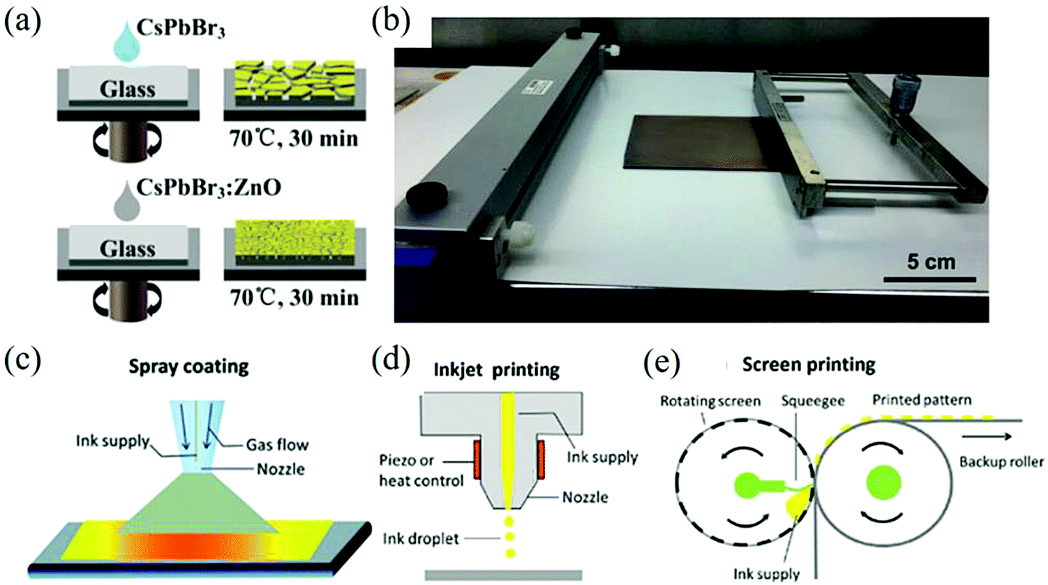 | ||
| Fig. 6 (a) Schematic diagram of the perovskite CsPbBr3 and CsPbBr3:ZnO films prepared by the one-step spin-coating method (Reproduced from ref. 90 with permission from 2017 Elsevier Ltd). (b) Blade-coating equipment with the as-prepared 10 × 10 cm perovskite film (Reproduced from ref. 96 with permission from 2015 WILEY-VCH). Schematic diagram of (c) spray coating, (d) pneumatic spraying, (e) screen printing (Reproduced from ref. 100 with permission from 2019 The Royal Society of Chemistry). | ||
Due to its low cost, doctor blading is widely used in large-area solution coating technology in the printing industry. At present, it has been widely used in the preparation of photovoltaic and photoelectric devices.91–94 When using the doctor blading process, the slurry mixed evenly is placed on the side of the substrate close to the blade and the blade passes through the surface of the substrate uniformly to spread the solution on the substrate. Usually, the film thickness can reach hundreds of microns, which is affected by the concentration of the solution, the surface energy of the substrate, coating speed, and the gap between the scraper and the substrate. It is easy to expand in large-scale industrialization and it is compatible with roll-to-roll setting.95Fig. 6b shows the a doctor blading equipment with a 10 × 10 cm perovskite film.96
Spraying refers to the atomization of the liquid material into tiny droplets through the nozzle and their even dispersion on the substrate to form a film. Generally speaking, spraying is controlled by the gas flow and nozzle size, and has flexible compatibility with various irregular substrates. This kind of common large-area film making methods in various industries can be divided into three categories: electric spraying, ultrasonic spraying, and pneumatic spraying. In the early research of PSC, ultrasonic spraying and pneumatic spraying have often been used for the interlayer deposition of dense oxides and ultrasonic spraying can also be used for the deposition of a photosensitive layer, as shown in Fig. 6c, which is the schematic diagram of pneumatic spraying.97–100
4.2 Printing
The ink-jet printing device uses at least one micro-nozzle to control the size and scanning trajectory of the ink droplets. The short distance between the nozzle and the substrate can provide strong resolution and print out more complex 2D images. Ink-jet printing is suitable for a variety of materials, such as organic materials, nanoparticles, perovskites, and biopolymers, and its flexible patterning capabilities are often used to print electronic products on a large area. The advantages of this process are as follows: printing is easy to pattern, reduces material consumption, no mask and non-contact deposition, cost-effective, and large-scale production capabilities; the schematic diagram of the ink-jet printing device is as shown in Fig. 6d.101,102Screen printing includes parts such as screens with specific patterns, inks, blade, and substrates. The schematic diagram of the simple device is as shown in Fig. 6e. The ink is usually placed on the silk screen and when the scraper moves, the ink is spread on the screen. Through screen holes in the pattern, the ink is transferred to the substrate to form the desired pattern. Although, this method can be used to easily and quickly prepare the pattern, it is still affected by factors such as the speed and angle of the blade during processing, the material of the screen, and the distance from the substrate.
5. Perovskite NC photodetectors
Halide perovskites can easily adjust the band gap from UV to NIR. According to the spectral response range of the photodetectors, it can be divided into two categories: broadband and narrowband. Broadband photodetectors are widely used in many industrial fields, such as remote sensing and environmental monitoring. When spectrally selective photodetectors are needed, such as those that only detect red, green, blue, or infrared light, and shielding other bands of light, we can refer to the concept of charge collection narrowing (CCN) proposed by Paul et al. and the required band can be selected without a filter.103The equipment architecture of the photodetectors can be divided into the lateral structure and the vertical structure according to the stacking mode of the functional layers.104 The schematic diagram is shown in Fig. 7. Photodetectors with a lateral structure have a photoconductor and a phototransistor. Their common characteristics are that the larger electrode spacing leads to higher driving voltage and slower time response, while the advantage is that it is easy to manufacture and has higher EQE and responsivity; the photodetector with a vertical structure is a photodiode with small electrode spacing, which is easy to obtain fast response speed and low driving current. In addition, Schottky junctions exhibit lower dark current but lower EQE. Obviously, each device structure has its own advantages and disadvantages. How to make full use of the advantages and avoid the disadvantages and give full play to the advantages of different structures in different fields of demand is worth exploring for flexible application.
 | ||
| Fig. 7 The schematic diagram of device configurations of (a) the vertical structure and (b) the lateral structure (Reproduced from ref. 104 with permission from 2013 Wiley-VCH). | ||
5.1 Photodiode
Photodiodes are mainly composed of p–n, p–i–n, or Schottky junction, forming a sandwich structure similar to that of photovoltaic devices. Due to the different work functions of the two electrodes, the photogenerated carrier pairs are controlled by the built-in electric field and separated when passing through the interface layer. Additional reverse bias is usually applied to improve the charge collection efficiency. Thanks to the existence of the interface layer, fast response and high detection rate can be obtained only by providing a low driving voltage. Meanwhile, the existence of junction barriers also leads to a low dark current. In particular, the structure of the device requires the electrode to be highly transparent so as to maximize the incident light that reaches the photosensitive layer.Zou et al. epitaxially blended MAPbBr3 QDs and PbSxSe1−x QDs to form PbS0.4Se0.6:MAPbBr3, which was employed as the active layer to prepare a broadband (UV-IR) photodetector.105 The performance of the resulting device is better than that of pure perovskite and traditional inorganic semiconductor photodetectors.106 The composite material not only extends the absorption range of the perovskite to the infrared region but also eliminates structural defects and trap states via heteroepitaxial growth. It combines the high charge transport properties of MAPbBr3 QDs and the high photosensitivity of PbS0.4Se0.6 QDs. Under 532 nm and 980 nm laser irradiation at room temperature, the maximum photoresponsivity and detectivity were 21.48 A W−1, 3.59 × 10¹³ Jones, and 22.16 A W−1, 3.70 × 10¹³ Jones, respectively, which were much higher than the control device with the structure of ITO/ZnO/PbS0.4Se0.6/MAPbBr3/Au. Although the excellent properties of the organic halide perovskite are widely sought after in the field of optoelectronic devices, the lack of reliability and stability in aqueous oxygen environment is still an important obstacle that restricts its application. In contrast, the colloidal all-inorganic halide perovskite has higher stability and better fault tolerance. Sim et al. prepared a high detectivity and no hysteresis α-CsPbI3 perovskite NCs photodiode, which can maintain its stability in a high humidity environment.107 In addition, as an electron barrier layer, P3HT can also passivate the interface defects. Fig. 8a and b show the energy level diagram and the cross-sectional transmission electron microscopy image of the device. The final diode showed a detectivity of 1.8 × 10¹² Jones and a noise equivalent power of 1.6 × 10⁻¹³ W Hz−0.5, which makes the ideal coefficient of the device as low as 1.5 (Fig. 8c and d).
 | ||
| Fig. 8 (a) Energy level diagram of the optimized photodiode in this work. (b) The cross-section transmission electron microscopy image of the optimized photodiode. The scale bar is 200 nm. (c) Detectivity and responsivity spectra. (d) Dark current vs. noise current of the photodiodes with and without the P3HT layer. The dashed line indicates the theoretical limits of the shot noise (Reproduced from ref. 107 with permission from 2017 Wiley-VCH). (e) Schematic illustration and TEM images of the changes after purification and AET ligand exchange performed on the CsPbI3 QDs. (f) Evolution of the responsivity of the photodetector monitored at 690 nm for up to 40 h for photodetectors based on CsPbI3 QDs (black curves) and AET-CsPbI3 QDs (red curves) (Reproduced from ref. 108 with permission from 2019 Wiley-VCH). | ||
Previously, Li et al. produced an LED with high QY through purification methods. Similarly, Bi et al. introduced short chain 2-aminoethanethiol (AET) into CsPbI3 QDs for partial ligand exchange with long-chain ligands oleic acid (OA) and oleylamine (OAM).108 It can not only passivate the surface traps of the QDs but also forms a dense barrier layer to prevent water molecules from entering the QDs. Schematic diagram of the changes after purification and AET ligand exchange on the CsPbI3 QDs is shown in Fig. 8e. The optimized device can maintain a cubic crystal structure and high optical performance for a long time, showing a high responsivity of 100 mA W−1, and the detectivity at 450 and 700 nm is 5 × 10¹³ Jones and 3 × 10¹³ Jones, respectively. Without encapsulation, the detector can maintain an initial responsivity of more than 95% in ambient air for 40 h (Fig. 8f).
The selective detection of solar-blind UV less than 300 nm is often used in remote security monitoring, flame detection, and other aspects.109,110 However, the expensive III–V crystal materials used in this field in the past restrict the promotion and application of the devices. In order to solve the problem of cost, Lu et al. used CsPbX3 QDs to convert ultraviolet light into a wavelength range suitable for silicon-based absorption and sensing.111 Then, a 3D hybrid structure was formed by silicon nanowire radial junction (SiNW RJ) to improve the light collection efficiency. The side walls of SiNW-RJ are uniformly covered with CsPbX3 QDs, which can generate powerful light field excitation and improve the UV down-conversion efficiency. Fig. 9a is the schematic diagram of the spin-coated CsPbX3 QDs film on the SiNW-RJ architecture. This QD-SiNW-RJ system realizes ultra-fast UV wavelength detection. The peak responsivity at 200 nm is 54 mA W−1 and the rise/fall time scale is 0.48/1.03 ms (Fig. 9b and c) without external power supply. It is expected to expand the low-cost and large-scale manufacturing of Si-based perovskite ultraviolet high-performance detectors. As UV-C (200–280 nm) light is easily absorbed by the glass or polymer substrate, direct UV-C light irradiation on the photodiodes will cause great light loss. Zou et al. indirectly modified the light source and developed a UV photodetector array by using CsPbBr3 QDs to convert high-energy photons into low-energy visible photons.112 The schematic diagram of the detection system is shown in Fig. 9d. Although this novel structure makes the down-conversion optical detection efficiency higher, the colorless polyimide (CPI) film as the substrate still reduces the intensity of the 510 nm light by nearly an order of magnitude; thus, there will still be more room for improvement.
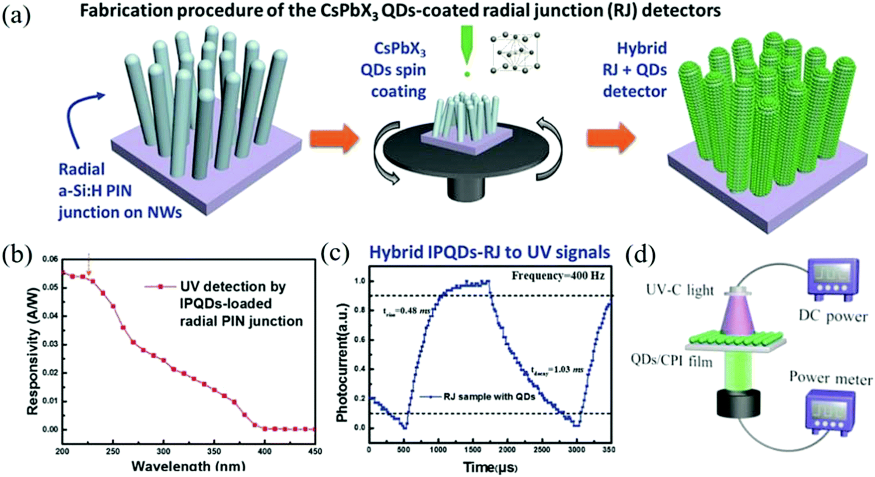 | ||
| Fig. 9 (a) Illustration of the spin-coating of the CsPbX3 QDs thin film over the 3D SiNW-RJ architecture with the corresponding SEM images of the RJ units. (b) The extracted net photocurrent responsivity to solar blind UV wavelengths. (c) The magnified and normalized plots of one response cycle (Reproduced from ref. 111 with permission from 2017 Wiley-VCH). (d) Schematic diagram of the integrated photodetection system comprising photodiode arrays and the CsPbBr3 QDs fluorophor (Reproduced from ref. 112 with permission from 2019 Wiley-VCH). | ||
The solution processability of perovskite materials not only reduces the manufacturing cost but also greatly expands the application range of the materials, such as wear-resistant devices, electronic skin, and other flexible devices.113–115 Due to the low transparency of perovskite films, the development of such applications is restricted.116,117 Jeon et al. turned their sights on nanoparticles and successfully prepared CH3NH3PbI3 NPs flexible photodetectors with high transparency on a polyethylene terephthalate (PET) substrate (as shown in Fig. 10a).118 Its light transmittance is above 80% in the visible light range (Fig. 10b) and the responsivity under red, green, and blue LEDs is 0.96, 2.02, and 4.92 mA W−1, respectively. This kind of device can maintain its initial performance after bending, which shows its advantages in flexible applications. With the in-depth research of perovskite optoelectronic devices, various types of high-performance devices emerge endlessly. However, these devices with excellent performance are still limited to the laboratory stage. Therefore, the large-scale, industrialized device manufacturing technology needs to be paid attention to. The spray-coating technology has attracted the attention of researchers because it can easily prepare large-area films on flat, curved, or even reticular substrates. Yang et al. developed a deposition rate of 9 nm s−1 in the spray technology, which can be used to prepare CsPbBr3 QDs photodiodes on flexible substrates.119 The schematic diagram of the spraying equipment is shown in Fig. 10c. It should be noted that the PCE value is still lower than that of the spin coating equipment and the surface roughness of the film should be further adjusted to optimize the spraying process.
 | ||
| Fig. 10 (a) Schematic diagram of the process of preparing CH3NH3PbI3 NPs flexible photodetectors with high transparency on the PET substrate and chemical structures of the TPBi and the TAPC organic layers. (b) Transmittance spectrum for the CH3NH3PbI3 perovskite NPs on 250 × 250 mm bare glass (Reproduced from ref. 118 with permission from 2017 Elsevier B.V.). (c) Schematic of the spray deposition equipment (Reproduced from ref. 119 with permission from 2018 American Chemical Society). | ||
5.2 Photoconductor
The photoconductor has a simple structure and the light response mechanism is equivalent to the photon–electron conversion process, which involves the photoconductivity effect. It is usually composed of two metal electrodes with ohmic contact sandwiched with the semiconductors. When the incident light irradiates the photosensitive material, the excited electron hole pairs can cycle through the symmetrical contacts several times before recombination. An incident photon can trigger multiple electrons to provide current. The photoconductivity gain is defined as the ratio of the charge recombination time (τr) to the charge transfer time (τt), which leads to efficiency greater than 100%, higher external quantum efficiency (EQE), and gain, thus leading to high sensitivity even for weak light. However, ohmic contact and the need to apply a large voltage will lead to a large dark current and slow response, which restricts the detection ability.Ramasamy et al. reported for the first time a photodetector based on CsPbI3 NCs and studied the halide exchange reaction of the Cl− or I− ion replacing Br− by CsPbBr3 NCs.11 The absorption range was adjusted to blue or red in the visible region (425–655 nm). This method is simple, rapid, and reproducible. Finally, as CsPbI3 NCs has longer radiation lifetime than CsPbCl3 NCs and CsPbBr3 NCs, it was selected to prepare the photodetector with excellent performance. The on/off current ratio of the device is 105 and the rise and decay times are 24 and 29 ms, respectively.
The photodetector made directly with CsPbBr3 QDs is insulated. Therefore, Zhou's team made photodetectors with metal/semiconductor metal I (MSM I) transverse structure with the help of TiO2 as the scaffold material.120 Using mesoporous TiO2 (mp-TiO2) and CsPbBr3 QDs double-layer composite film as the light-absorbing layer, the on/off ratio was improved by nearly three orders of magnitude than that of pure bromine-based perovskite device with MSM II structure and the photoresponsivity was increased by about 44 times (80 mA W−1 increased to 3500 mA W−1). Fig. 11a shows the structure of MSM I and MSM II and the working mechanism of MSM I (Fig. 11b). When light is incident on the surface of the QDs, a large number of electrons generated by the photons flow into the n-type material mp-TiO2 through the interface between the QDs and TiO2 to form the photocurrent. In addition, photogenerated holes will remain on the surface of the CsPbBr3 QDs. This photogenerated charge transfer process provides a high-performance operation way. The energy level diagram also shows that the energy level of mp-TiO2 is between the Au electrode and CsPbBr3 QDs, which provides a charge transfer channel (Fig. 11c and d).
 | ||
| Fig. 11 (a) Schematic 3D view of the fabricated all-inorganic perovskite-based photodetectors. (b) Schematic illustration and (c) energy diagram of the operation mechanism of the MSM I photodetector, and (d) energy level diagram of different materials used in this study (Reproduced from ref. 120 with permission from 2017 The Royal Society of Chemistry). (e) A schematic 3D view of the CsPbBr3 QDs/mp-TiO2 hybrid photodetector; the right-hand side figure is the enlarged part. (f) Kinetic scheme that describes the excited-state process in the QDs-MPA-TiO2 system upon QDs excitation (Reproduced from ref. 123 with permission from 2017 The Royal Society of Chemistry). | ||
For the optimization of mp-TiO2-based double-layer composite structure, there is still a large scope for improvement. A variety of surface modifier materials (such as 3-mercaptopropionic acid (MPA), thioacetamide (TAA), and 1,2-ethanedithiol (EDT)) can be used for ligand exchange.121,122 In the same year, the team used MPA to treat CsPbBr3 QDs and prepared CsPbBr3 QDs/mp-TiO2 hybrid photodetectors with bifunctional molecular connection.123 The 3D schematic diagram of the hybrid photodetector is shown in Fig. 11e. The device after ligand treatment shows a faster electron injection speed and the kinetics scheme is shown in Fig. 11f. Because MPA is the electron transfer medium between QDs and TiO2, the electron transfer time is increased to less than 40 ns, which is higher than the direct transfer between the QDs and TiO2. In addition, MPA can also help mp-TiO2 adsorb more QDs. Compared with the control photodetectors without MPA, the responsivity of the photodetectors increased by 10 times to 24.5 A W−1 and the detectivity increased from 3.5 × 10¹² Jones to 8.9 × 10¹³ Jones. Moreover, the on/off ratio was up to 105, which was two orders of magnitude higher than that of the control group. This indicates that the electron injection rate plays an important role in the performance of the devices and it also indicates that there is still a wide scope for improvement.
Zheng et al. introduced the TiO2 nanotube array (NTs) into the organic–inorganic perovskite MAPbI3 QDs.85 The response range of the device is extended from UV to visible light (300–800 nm) by a simple spin coating process, which not only maintains the light response in the UV range but also improves the light response in the visible region by three orders of magnitude. However, perovskite exposed to UV light will produce UV photobleaching and the instability of MAPbI3 QDs in the environment still needs to be further improved.124 ZnO was first combined with CsPbCl3 QDs by Zhang et al., on which a UV photodetector with a visible light transmittance of 90% was achieved.125 After 1000 on/off cycles, the responsivity of the device was 1.89 A W−1, the on/off ratio was as high as 103, and the rise and decay times were 41 ms and 43 ms, respectively. Overall, it shows good stability and fast response. In order to expand the spectral response range, Zhang et al. selected up-conversion materials (NaYF4:Yb, Er QDs) to modify the surface of the α-CsPbI3 QDs and prepared an air-stable broadband photodetector from ultraviolet to near infrared region (260–1100 nm).126 It is amazing that the excellent stability of the QDs can be exposed to 30% RH and 25 °C for two months. It was confirmed that the lattice structure of CsPbI3 can be stabilized by the QDs and the stability is better than that of bulk CsPbI3.
Plasma modulation of metal nanoparticles has been widely used to improve the luminescence of QDs.127 Since the peak of local surface plasmon resonance (LSPR) matches the excitation/emission wavelength of the perovskite NCs, it can be used as a way to optimize the film for manufacturing perovskite optoelectronic devices.128 Dong et al. introduced this concept for the first time in the field of inorganic perovskite photodetectors.129 The typical plasmon peak of Au NCs is located at 530 nm, which is consistent with that of the CsPbX3 perovskite (380–700 nm). CsPbBr3 NCs can be prepared by recrystallization first and then, LSPR can be generated by adding Au NCs, which can enhance the photocurrent and realize the synergistic effect of preferential orientation film and plasmon. After the finite difference time domain simulation analysis of local light field plasmon resonance enhancement, it is found that the enhanced electric field can be obtained by introducing Au into NCs, as shown in Fig. 12a and b. With the enhancement of the Au NCs plasma, the enhancement factor of this device reaches 238% and the on/off ratio is greater than 106 (Fig. 12c). The above-mentioned Au plasma modulated detector has a dark current of 10−7 A. Li et al. used Ag plasma to prepare a flexible ultraviolet detector with a dark current as low as 10−11 A.130 At first, the QY of blue CsPbCl3 NCs is always difficult to be effectively improved due to the high density of the deep defect states caused by Cl− vacancy (the QY is about 5–10%) but the method of improving the PL only by doping has little effect (such as Mn2+ or rare earth ions).131 Therefore, the Ag plasma and PMMA opal photonic crystal were combined to improve the emission of blue CsPbCl3 NCs through the synergistic effect of surface plasmon and photonic crystal effect. The structural diagram is shown in Fig. 12d. Amazingly, the device's luminous intensity is increased by about 150 times, with an estimated emission efficiency of 51.5% and a response time of 28 ms/31 ms (Fig. 12e), which outperforms traditional silicon ultraviolet detectors.
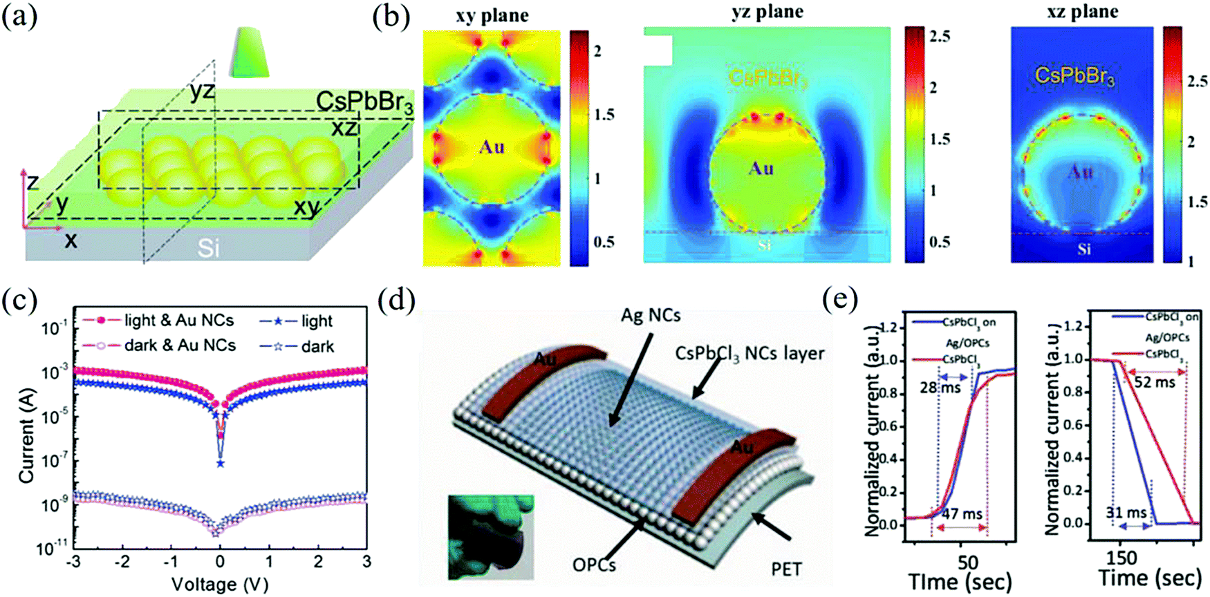 | ||
| Fig. 12 (a) The simplified schematic structures of the simulation model. (b) Finite-difference time-domain (FDTD) simulation of the plasmon resonance enhancement of local optical field at a resonant wavelength of 532 nm. (c) Measured I–V characteristics of the two devices under 532 nm laser (4.65 mW cm−2) (Reproduced from ref. 129 with permission from 2016 Wiley-VCH). (d) Schematic of CsPbCl3 on the Ag/OPCs photodetector. (e) Time-resolved photocurrent of the fabricated photodetector. (Reproduced from ref. 130 with permission from 2018 Wiley-VCH). | ||
In order to promote the colloidal perovskite nanocrystal photodetector, Jang et al. developed a novel ultrasonic induced synthetic method for the simple synthesis of APbX3 perovskite NCs with multiple compositions.132 This method uses ultrasonic radiation to accelerate the dissolution of the precursors (AX and PbX2) in toluene, thus accelerating the growth rate of the nanocrystals, which can be used to prepare materials flexibly and efficiently. They spin-coated APbBr3 and APbI3 NCs between the Au electrodes patterned on a silicon substrate to prepare a photodetector. It is expected that this technology will be extended to the large-scale production of high-sensitivity photodetectors in the future.
5.3 Phototransistor
A phototransistor is mainly determined by two quality factors, namely, photoconductive gain and responsivity, which are affected by the inherent characteristics of the channel materials. A phototransistor is a three-terminal device with a source electrode, a drain electrode, and a gate electrode. The gate is separated by the dielectric layer, which is used to modulate the carrier concentration in the channel in order to adjust the output source leakage current (IDS). The entire device can be regarded as a parallel plate capacitor formed by the gate and the semiconductor layer sandwiching the insulating layer. When the gate voltage is applied, holes or electrons are induced in the semiconductor layer so that charge transfer is modulated, thus increasing the carrier lifetime, reducing the noise signal, and amplifying the electrical signal. It is helpful for improving the reliability and gain of the phototransistor.Due to the weak light absorption and narrow response range of CsPbBr3 QDs, most of the reported phototransistors based on CsPbBr3 QDs often show low responsivity and long response time (in microseconds).133 Yu et al. combined PbS QDs, which have strong absorption ability in near-infrared light, with CsPbBr3 QDs and prepared CsPbBr3-PbS CQDS heterostructure phototransistors.134 The schematic diagram of the device structure is as shown in Fig. 13a. The channel length and channel width are defined as 0.1 mm and 2.5 mm, respectively, and the optimal thickness of the CsPbBr3 QDs film as the channel material is ≈15 nm. The transmission characteristic curve of the phototransistor is shown in Fig. 13b, which shows that the device has bipolar characteristics and the CsPbBr3/PbS heterojunction effectively promotes the separation of photogenerated excitons. This hybrid structure can achieve a wide spectral response from 400 to 1500 nm, showing a responsivity of up to 4.5 × 10⁵ A W−1 and a detectivity of 7 × 10¹³ Jones, with rise and decay times of ≈6.5 ms and 7.5 ms (Fig. 13c). In addition, the performance is stable and repeatable during the cycle-switching process. Chen et al. integrated dinaphtho[2,3-b:2′,3′-f]thieno[3,2-b]thiophene (DNTT) with CsPbBr3 QDs to construct a hybrid phototransistor in order to solve the defect of low conductivity.135 DNTT molecules are orderly stacked on the surface of the QDs layer, which provides a fast transmission path of photogenerated charge through DNTT. The light responsivity reaches 1.7 × 10⁴ A W−1, the detectivity is 2 × 10¹⁴ Jones, and it also has high signal-to-noise ratio. It can be stored in ambient air for 100 days, showing its advantages in stability. Zou et al. also prepared CsPbI3 QDs and DPP-DTT narrow-band conjugated polymer phototransistors with the help of a layered heterojunction (LHJ).136 The LHJ strategy helps to separate the electrons and holes into different paths, which makes it easy to extract the generated carriers and increase the photocurrent. Combined with the gate modulation characteristics, the phototransistor achieves a responsivity of up to 110 A W−1, a detectivity of 2.9 × 10¹³ Jones, and good switching characteristics (the light–dark current ratio is 6 × 10³) in a wide spectral range (350–940 nm).
 | ||
| Fig. 13 (a) The schematic diagram of the CsPbBr3-PbS hybrid phototransistor architecture. (b) Logarithmic plot of the transfer characteristics of the typical CsPbBr3 phototransistors, before (in darkness) and after PbS QDs decoration (in darkness and under illumination of 845 mW cm−2) with VDS = 0.24 V applied bias voltage. (c) Temporal photocurrent responses highlighting a rise time of 6.5 ms and a decay time of 7.5 ms (Reproduced from ref. 134 with permission from 2017 Wiley-VCH). (d) Schematic diagram of the organic-QDs photodetector (left). Energy level diagram of the CsPbBr3 QDs, Poly-TPD, and PCBM (right). (e) Transient absorption kinetics of the multilayer film and the pure QDs film. (f) Charge transfer kinetics in the organic/QDs/organic multilayer film (Reproduced from ref. 138 with permission from 2019 Wiley-VCH). | ||
The polymer PC71BM can provide electron acceptor sites to selectively extract and capture electrons from the CsPbBr3 NCs, thus promoting the separation rate of exciton generation. The carrier mobility of CsPbBr3:PC71BM hybrid phototransistors fabricated by Li et al. is μn = 20.35 cm2 V−1 s−1 and μP = 21.22 cm2 V−1 s−1, respectively, showing excellent transmission capacity.137
The combination of a variety of polymers may also have a strengthening effect. A sandwich type mixed membrane with the CsPbBr3 QDs layer between PCBM and poly(N,N′-bis-4-butylphenyl-N,N′-bisphenyl)benzidine (Poly-TPD) was reported by Li and his colleagues.138 This hybrid film facilitates the rapid transfer of charges from the inorganic QDs to the organic material and the organic material turns the heterojunction with high energy barrier into an ohmic contact. Adding a protective layer from the hydrofluoroether solution (M7100) solves the problem of solvent orthogonality (Fig. 13d).139–141 The transient absorption spectroscopy (TAS) measurements further reveal the carrier dynamics (such as carrier transfer, recombination, and relaxation).142,143 The device exhibits fast charge transfer (time about 300 ps), reduced trap assisted carrier recombination, and dark current (NEP is 1 × 10⁻¹⁶ W Hz−0.5). The kinetic trajectories of QDs in pure QDs and the organic/QDs/organic structure are shown in Fig. 13e and the dynamic process of charge transfer at the interface between the QDs and the organic layer is shown in Fig. 13f. Ren et al. also doped P3HT and the indene-c60 bisadduct (ICBA) into the CsPbBr3 QDs to suppress the dark current and improve the charge carrier mobility.144
Due to the low carrier mobility of the perovskite NCs-based photodetectors, there have been reports on the hybridization between graphene and semiconductor NCs, such as the mixing of graphene and PbS QDs.139,145–148 Kwak and colleagues introduced graphene with a carrier mobility of ∼2 × 105 cm2 V−1 s−1 into the CsPbBr3−xIx NCs photodetector framework.149 The shift in the Dirac point and the band bending of graphene indicate the transfer of holes from the CsPbBr3−xIx NCs to graphene. When the incident power is 0.07 μW cm−2 at 405 nm, the responsivity and detectivity are as high as 8.2 × 10⁸ A W−1 and 2.4 × 10¹⁶ Jones, respectively. However, they also reported that the device had a slow rise and decay times (up to a few seconds) and still needed to address the ligand-related issues.
Liu et al. developed a highly-efficient graphene perovskite phototransistor that significantly improved the switching ratio.150 The structure and fabrication processes of the GNR/CsPbBr3 QDs/IGZO phototransistors are shown in Fig. 14a. By constructing the graphene nanoribbon (GNR)/CsPbBr3 QDs/IGZO vertical heterostructure, electrons are driven through the electron transport layer IGZO and holes are trapped in the QDs/graphene nanoribbons by IGZO, which can be used as the hole blocking layer. In addition, the enhanced electric field at the edge of the nanoribbons also improves the photoelectric properties and the on/off ratio of >103 is obtained. In order to avoid the inherent phase instability of CsPbI3, Surendran et al. selected halogen ion-exchanged CsPbBrxI3−x NCs as the light absorber and graphene as the transporter to prepare a high-stability phototransistor.151,152Fig. 14b shows the schematic diagram of the device structure. The TEM image of the anion-exchanged CsPbBrxI3−x NCs shown in Fig. 14c demonstrates that NCs can maintain a cubic lattice structure with excellent performance, and the mixed halide NCs will not produce ion separation and halide segregation domains under low light intensity. The phototransistor can show about 82% photocurrent after 37 h and the stability can be maintained for up to 2 weeks. Besides, Gong et al. used MPA to passivate the surface of the CsPbCl3 NCs and prepared a UV phototransistor with the structure of CsPbCl3 NCs/graphene for visible-blind ultraviolet detection (wavelength below 400 nm).153Fig. 14d shows the PL spectra of CsPbCl3 NCs before and after the MPA ligand exchange. It can be seen that after passivation, the PL peak of the CsPbCl3 NCs at 407 nm disappears due to the recombination of radiation electron–hole pairs. The optimized device can maintain stability for more than 2400 h under environmental conditions and can withstand 25 bending cycles when extended to the flexible PET substrate (Fig. 14e). Pan et al. combined the long charge carrier lifetime of organic–inorganic halide perovskite FAPbBr3 QDs with the high mobility of graphene to prepare the devices.154 Under the illumination power of 3 μW with a wavelength of 520 nm, the light response is 1.15 × 10⁵ A W−1 and the EQE is as high as 3.42 × 10⁷%. This high performance is also due to the specific photoconductive gain mechanism (photo-gating effect) generated by the trapped carriers in the FAPbBr3 QDs.155
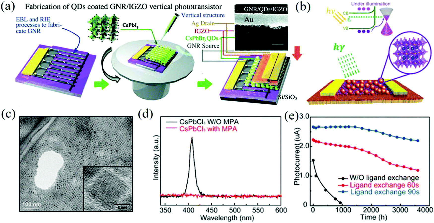 | ||
| Fig. 14 (a) Structure and fabrication processes of the GNR/CsPbBr3 QDs/IGZO phototransistors. The corresponding SEM image of the device (inset, scale bar: 1 μm) (Reproduced from ref. 150 with permission from 2018 The Royal Society of Chemistry). (b) Schematic of the hybrid phototransistor with the inset showing the crystal structure of the NCs with Cs (blue), Pb (yellow), and Br/I (pink). (c) The TEM image of the anion-exchanged CsPbBrxI3−x NCs. The inset shows the magnified image of a single NC (Reproduced from ref. 152 with permission from 2019 American Chemical Society). (d) Comparison of the PL emission spectra of the CsPbCl3 NCs as synthesized (black) and after the MPA ligand exchange (red) in hexane. (e) Photocurrent measured on CsPbCl3 NCs/GFET photodetectors without and with passivation under ambient conditions (Reproduced from ref. 153 with permission from 2019 American Chemical Society). | ||
Transition metal carbon disulfide (TMDC) has been extensively studied and applied in optoelectronic devices due to its adjustable energy band gap, high charge mobility, and luminescence characteristics.156–158 As a typical TMDC system material, 2D molybdenum disulfide (MoS2) has a direct band gap of 1.8 eV and a mobility of 0.1–3 cm2 (V s)−1.139 Wu et al. used the band alignment protocol to construct 0D–2D MvdWH phototransistors with typical type I and type II electronic structures, where 0D–2D are the perovskite QDs and the MoS2 monolayers, respectively.159 It was confirmed that the performance of the PFET-II device is better than that of the PFET-I device, the optical gain is more than 105, the light response is as high as 5.5 × 10⁴ A W−1, and the detectivity reaches 1.95 × 10¹² Jones. In the same year, they used 2D-transition metal dihydrogen disulfide (2D-TMD) and CsPbI3−xBrx QDs with excellent flexibility to construct 0D–2D MvdWH photodetectors.160
In order to solve the surface passivation problem of the perovskite NCs film, Li et al. skillfully proposed a recyclable dissolution recrystallization optimization method according to the ionic characteristics of CsPbBr3 in the solvent.161,162 This phenomenon can transfer the material from the sharp part of the surface to the gap at room temperature to form a self-healing process so that large-area perovskite films without cracks can be prepared (Fig. 15a and b). The smooth surface of the CsPbBr3 film can promote the transport and extraction of the photogenerated carriers in the channel, and the rise and decay times are 1 ms and 1.8 ms, respectively (Fig. 15c). In addition, the smooth surface of the film also improves the stability of the film. It provides a broader idea for the research of perovskite photodetectors.
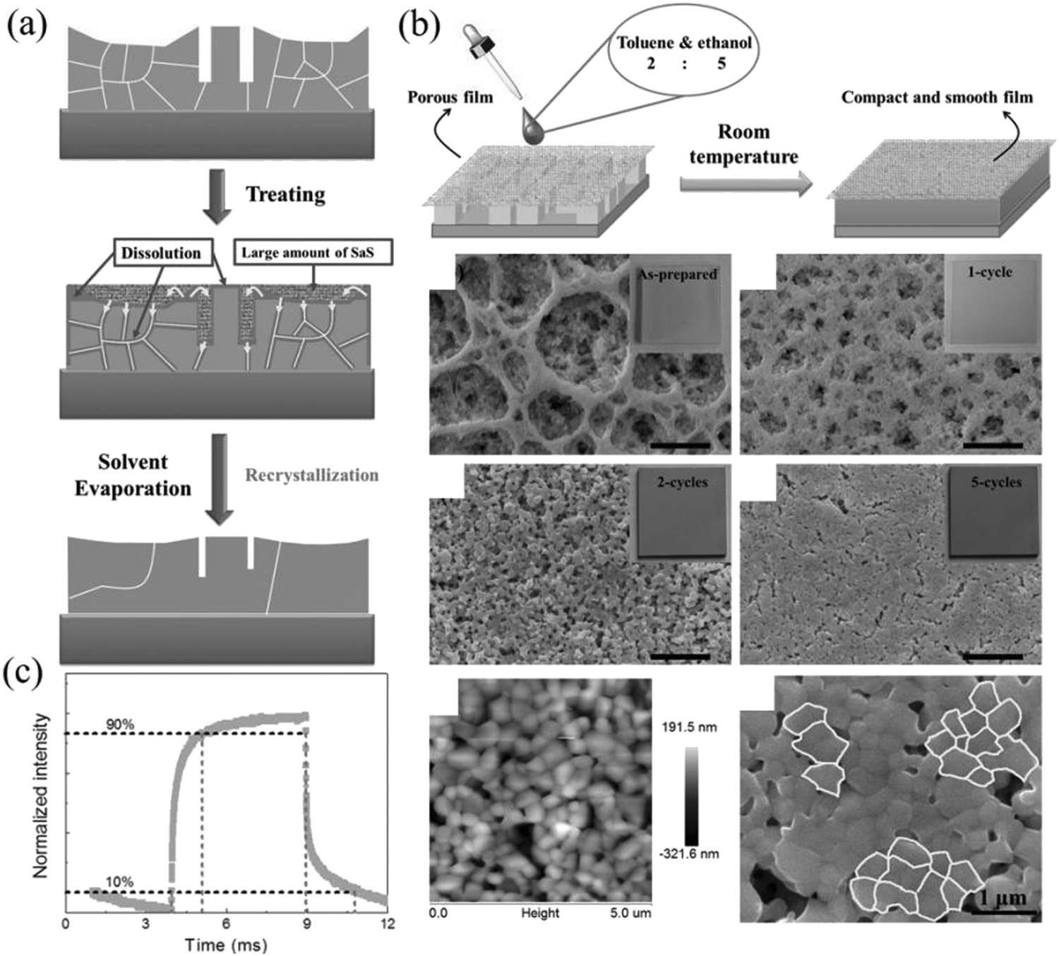 | ||
| Fig. 15 (a) Proposed film modification mechanism. (b) Healing all-inorganic perovskite films via RDR. Schematic of the operation process of film modification. SEM and AFM images of the treated films. (c) PD at a light intensity of 1.01 mW cm−2 (Reproduced from ref. 162 with permission from 2016 WILEY-VCH). | ||
Although halide perovskite NCs have high device performance, the Pb element has the risk of causing pollution to the environment and its toxicity to the human body cannot be underestimated. The European Union has officially announced that it has regulated the use of hazardous substances (including lead) in electronic equipment, which will form a global trend. Therefore, lead-free perovskite NCs are expected in large-scale applications. Numerous research groups have carried out the exploration of lead-free perovskite NCs. The current research focuses on replacing Pb with Ge, Mn, and Sn, and has achieved varying degrees of results.131,163–166 Although these low-toxic multivalent cations are environment-friendly, their limitations are also very prominent, such as the low PL quantum yield caused by a large number of inherent defect sites and the high exciton binding energy reduces its exciton dissociation rate. In recent years, with the in-depth research on environment-friendly perovskite NCs photodetectors, a number of photoelectric devices with enhanced performance have emerged.
Usually, Sn2+ is very easy to be oxidized to Sn4+ in air, resulting in poor stability of the device.167 In recent years, there have been studies that directly use air-stable Sn4+ to prepare field-effect transistor devices, such as Cs2SnI6 NCs, so that the devices can remain stable under the condition of an ambient humidity of 60%, and show high ION/IOFF ratio (>104) and high hole mobility (>20 cm−2 V s−1). Besides, Cs2SnI6 NCs without organic ligands can exhibit enhanced stability by optimizing the synthetic method and the conductivity of the device can also be improved due to the high quality of the film.168
Subject to the fact that Group 14 elements such as Pb substitutes generally show poor stability, the stability of Bi and Sb as trivalent substitutions has attracted much attention, such as Cs3Bi2Br9 NCs under different synthetic strategies. There are some reports that have introduced the stability of Cs3Bi2Br9 NCs in different environments, for example, it is stable in air for 30 days, heated at 180 °C for 1 h, and kept 80% of the PL value in the presence of water vapor for 8 h.169–171 The Cs3Sb2Br9 NCs can also maintain 70% of the original PL value after 35 days of aging. In contrast, the Sb halide perovskite NCs have more defect sites.172 Therefore, in order to solve these problems, highly crystalline CsYbI3 NCs with high light responsiveness (2.4 × 10³ A W−1) and EQE (5.8 × 10⁵%) were prepared by a simple thermal injection method. The low exciton binding energy of CsYbI3 NCs is helpful for exciton dissociation at the interfaces. In addition, CsYbI3 NCs, by combining with graphene with high charge mobility as a channel, can achieve high-performance photodetectors.173
However, the emergence of mixed cations (A2BB′X6) lead-free perovskite NCs produced by B-position substitution has made a breakthrough in stability. For example, Cs2AgBiBr6 can be kept for 90 days in an environment with a relative humidity of 55%, and it also shows high stability under light and heat conditions.174 It is worth mentioning that Cs2AgInX6, Cs2AgSbX6 (X = Br, I, or Cl) NCs, as well as Mn and Cu doping systems, also show their own advantages in different performances.175–177
Table 1 summarizes the device performance of perovskite NCs detector in this paper.
| Structure | Device configuration | Response range (nm) | R (A W−1) | D* (Jones) | Rise/decay time (ms) | Ref. |
|---|---|---|---|---|---|---|
| Photodiode | ITO/ZnO/PbS0.4Se0.6:MAPbBr3/Au | 980 | 22.16 | 3.70 × 10¹³ | NA | 100 |
| ITO/ZnO/α-CsPbI3/P3HT/MoO3/Ag | 640 | 0.035 | 1.8 × 10¹² | 0.112 | 102 | |
| FTO/TiO2/CsPbI3 QDs/spiro-OMeTAD/Ag | 300–720 | 0.1 | 3 × 10¹³ (700 nm) | NA | 103 | |
| CsPbX3 QDs/a-Si radial PIN junction/glass | 200–400 | 0.054 (200 nm) | NA | 0.48/1.03 | 106 | |
| 0.032 (270 nm) | ||||||
| CsPbBr3 QDs/CPI/ITO/CH3NH3PbI3/PCBM/BCP/Au | 279 | 0.0014 | 2.4 × 10¹¹ | <1 | 107 | |
| FTO/TiO2/CsPbBr3 QDs/Spiro-OMeTAD/Au | 365 | 3 | 1 × 10¹⁴ | NA | 114 | |
| Photoconductor | CsPbBr3-MPA(mp-TiO2) | 400–550 | 24.5 | 8.9 × 10¹³ | 4700/2300 | 118 |
| TiO2 NTs/MAPbI3 QDs | 700 | 0.189 | 3.8 × 10¹¹ | 7000/4000 | 80 | |
| CsPbCl3 NCs | 300–410 | 1.89 | 17.5 | 41/43 | 120 | |
| NaYF4:Yb, Er QDs/α-CsPbI3 QDs | 260–1100 nm | 1.5 | NA | 5/5 | 121 | |
| CsPbBr3 NCs/Au NCs | 532 | 0.01004 | 4.56 × 10⁸ | 0.2/1.2 | 124 | |
| CsPbCl3/Ag/OPCs | 365 | 8.1 | 9 × 10¹⁴ | 28/31 | 125 | |
| Phototransistor | CsPbBr3 QDs/PbS QDs | 400–1500 | 4.5 × 10⁵ | 7 × 10¹³ | 6.5/7.5 | 129 |
| CsPbBr3 QDs/DNTT | 460 | 1.7 × 10⁴ | 2 × 10¹⁴ | NA | 130 | |
| CsPbI3 QD/DPP-DTT | 350–940 | 110 | 2.9 × 10¹³ | 3200/3300 | 131 | |
| CsPbBr3 NCs/PC71BM | 405 | 1.72 | 1.76 × 10⁷ | 0.09/0.1 | 132 | |
| PCBM/CsPbBr3 QDs/Poly-TPD | 450 | 0.4 | 4.6 × 10¹³ | <25 | 133 | |
| Graphene-CsPbBr3−xIx NCs | 405 | 8.2 × 10⁸ | 2.4 × 10¹⁶ | 810/3650 | 144 | |
| GNR/CsPbBr3 QDs/IGZO | 512 | 1 × 10⁵ | 7.5 × 10¹⁴ | 0.068/0.074 | 145 | |
| ITO/NiO/CH3NH3PbI3/PCBM/LiF/Al | 525 | 1.13 × 10⁴ | 1.17 × 10¹¹ | 273.6/2260 | 147 | |
| MPA-CsPbCl3 NCs/GFET | <400 | 106 | 2 × 10¹³ | 300/350 | 148 | |
| FAPbBr3 QDs/graphene | 660–980 | 1.15 × 10⁵ | NA | 58/60 | 149 | |
| CH3NH3PbBr3 QDs/2D-MoS2 | NA | 5.5 × 10⁴ | 1.95 × 10¹² | NA | 154 | |
| CsPbI3−xBrx QDs/2D-TMD | 532 | 7.7 × 10⁴ | 5.6 × 10¹¹ | 590/320 | 155 | |
| Au/CsPbBr3 NCs/Au | 442 | 0.18 | 6.1 × 10¹⁰ | 1.8/1.0 | 157 | |
6. Conclusions and outlook
Perovskite NC materials have excellent performance in light collection and emission due to their unique photoelectric characteristics, and are suitable for playing their special role in the field of photoelectric appliances. In this paper, we summarize the latest progress in the synthesis of perovskite NCs, its passivation after synthesis, and its role in photodetectors. With previous efforts, novel synthetic strategies have been developed under different environmental conditions, such as room temperature, high temperature, and even ultrasound. Although many methods can be used to synthesize the NCs, there are still many challenges. The synthesized NCs are not uniform in size, fluctuate greatly under the influence of temperature and time, and vary from batch to batch. After the synthesis of NCs, they are affected by the environment and their own stability, and phase transition occurs, which affects the photoelectric performance. In terms of material utilization, precursor materials face considerable wastage because they need to be cleaned after synthesis before they can participate in the reaction. These unfavorable factors are still waiting to be solved and improved.Although perovskite NCs are more stable than 3D perovskites, they are still affected by the route of NC synthesis and packaging. Choosing appropriate ligands during the synthetic process not only maintains the structure and dispersion of NCs but also affects their conductivity and stability. In addition, the appropriate solvent and appropriate number of times are needed to clean the ligand. Incomplete cleaning hinders carrier transport, while excessive cleaning destroys dispersion in the solvent and introduces surface defects. Using stable materials to form a protective layer around the NCs is also a common strategy to improve the stability. Oxide coatings with low ionic diffusivity, such as SiO2 and TiO2, are coated on the surface of the perovskite layer to isolate oxygen and water molecules but at present, there are defects such as pinholes on the surface of the coating. NC materials can be embedded in a suitable polymer matrix and the passivation of the NCs surface by carboxyl or amine groups not only enhances the PL performance but also prevents water vapor invasion; however, this improvement does not include thermal stability. Another mechanism to prevent water-oxygen penetration is to shorten the distance between the polymers through covalent bonds to form a dense film. In short, in situ growth is the most commonly used strategy to introduce stable materials and control the size and distribution of the NCs. However, its problems cannot be ignored, such as how charge can be successfully extracted and transported between different materials, which is an important basis for evaluating the quality of photoelectric devices. Perhaps the passivation effect of inorganic salts can provide different answers, or the barrier layer of the new material system can effectively inhibit the outside invasion and reduce the interference with the perovskite system itself. Therefore, can perovskite NCs make themselves more reliable?
In recent years, the research results of perovskite NCs in the field of optoelectronic devices have shown explosive growth, showing the recognition of researchers in this field on the side, and are continuously attracting more teams for further exploration. We can be glad to see the future of this field in everyday life. At this stage, there is still a difficult road to industrialization that needs to be crossed. From the material point of view, the perovskite material itself is sensitive to water, oxygen, and temperature, and the cornerstone of the device still needs to be reinforced. Similar to building a skyscraper, in addition to the excellent performance of the building's cornerstones, the design of its auxiliary materials and main frame determines the quality of the building. From the perspective of photodetectors, it is the transport layer and barrier layer that can be used to construct good carrier channels and reduce traps. In addition, in order to achieve special functions or improve the device performance, the structure of multiple devices in series has become a common strategy to create personalized applications. By cleverly choosing devices with complementary advantages to work together, the cost and difficulty of retrofitting the devices themselves are eliminated.
However, another obstacle in the market-oriented application of perovskite NCs is lead toxicity, which is currently difficult to eliminate. The interaction between the Pb component and the halogen component in the halogen perovskite maintains the stability of the overall structure, and the special band structure formed makes the perovskite defect-tolerant; thus, the materials containing the Pb component exhibit relatively higher performance. Based on the requirements of environment-friendly devices, many materials such as tin, germanium, and copper have been used to synthesize environment-friendly perovskite instead of Pb. Although these materials have good light absorption and carrier transport properties, they are still affected by unstable factors, such as Sn2+ in air, which is easy to be oxidized to Sn4+. Therefore, there is still a long way to explore environment-friendly perovskite NCs. The commercialization of perovskite NC minerals necessarily requires large-area preparation technology, which, together with inkjet printing, scratching, roll-to-roll printing, and other technologies, will adjust the materials and manufacturing equipment to an optimal state and also occupy an important position in this industry. To sum up, we need to work together in all aspects to overcome the difficulties encountered towards the road of development. Also, with the present and future research of many industry researchers, it is hoped that perovskite NC optoelectronic devices will contribute to the future of human society.
Conflicts of interest
There are no conflicts to declare.Acknowledgements
This work was supported by the National Natural Science Foundation of China (61774122), the Key Science and Technology Developing Project of Shaanxi Province (2020KWZ-004), and the 111 Project of China (B14040).References
- F. P. García de Arquer, A. Armin, P. Meredith and E. H. Sargent, Nat. Rev. Mater., 2017, 2, 16100 CrossRef.
- J. Michel, J. Liu and L. C. Kimerling, Nat. Photonics, 2010, 4, 527–534 CrossRef CAS.
- A. Rogalski, J. Antoszewski and L. Faraone, J. Appl. Phys., 2009, 105, 091101 CrossRef.
- K. Akihiro, T. Kenjiro, S. Yasuo and M. Tsutomu, J. Am. Chem. Soc., 2009, 131, 6050–6051 CrossRef.
- M. A. Green, Y. Jiang, A. M. Soufiani and A. Ho-Baillie, J. Phys. Chem. Lett., 2015, 6, 4774–4785 CrossRef CAS.
- Z. Guo, Y. Wan, M. Yang, J. Snaider, K. Zhu and L. Huang, Science, 2017, 356, 59–62 CrossRef CAS.
- Y. Zhao and K. Zhu, Chem. Soc. Rev., 2016, 45, 655–689 RSC.
- H. Wang and D. H. Kim, Chem. Soc. Rev., 2017, 46, 5204–5236 RSC.
- A. Miyata, A. Mitioglu, P. Plochocka, O. Portugall, J. T.-W. Wang, S. D. Stranks, H. J. Snaith and R. J. Nicholas, Nat. Phys., 2015, 11, 582–587 Search PubMed.
- NREL Best Research-Cell Efficiencies, https://www.nrel.gov/pv/assets/pdfs/best-research-cell-efficiencies.20190802.pdf.
- P. Ramasamy, D. H. Lim, B. Kim, S. H. Lee, M. S. Lee and J. S. Lee, Chem. Commun., 2016, 52, 2067–2070 RSC.
- D. Ghosh, M. Y. Ali, D. K. Chaudhary and S. Bhattacharyya, Sol. Energy Mater. Sol. Cells, 2018, 185, 28–35 CrossRef CAS.
- G. Kieslich, S. Sun and A. K. Cheetham, Chem. Sci., 2015, 6, 3430–3433 RSC.
- Y. Liu, Z. Yang and S. F. Liu, Adv. Sci., 2018, 5, 1700471 CrossRef.
- F. Brivio, J. M. Frost, J. M. Skelton, A. J. Jackson, O. J. Weber, M. T. Weller, A. R. Goñi, A. M. A. Leguy, P. R. F. Barnes and A. Walsh, Phys. Rev. B: Condens. Matter Mater. Phys., 2015, 92, 144308 CrossRef.
- D. A. Egger, A. M. Rappe and L. Kronik, Acc. Chem. Res., 2016, 49, 573–581 CrossRef CAS.
- M. A. Green, A. Ho-Baillie and H. J. Snaith, Nat. Photonics, 2014, 8, 506–514 CrossRef CAS.
- C. Li, X. Lu, W. Ding, L. Feng, Y. Gao and Z. Guo, Acta Crystallogr., Sect. B: Struct. Sci., 2008, 64, 702–707 CrossRef CAS.
- D. B. Mitzi, S. Wang, C. A. Feild, C. A. Chess and A. M. J. e. Guloy, Science, 1995, 267, 1473–1476 CrossRef CAS.
- S. Wang, D. B. Mitzi, C. A. Feild and A. Guloy, J. Am. Chem. Soc., 1995, 117, 5297–5302 CrossRef CAS.
- H. S. Kim, S. H. Im and N. G. Park, J. Phys. Chem. C, 2014, 118, 5615–5625 CrossRef CAS.
- L. Protesescu, S. Yakunin, M. I. Bodnarchuk, F. Krieg, R. Caputo, C. H. Hendon, R. X. Yang, A. Walsh and M. V. Kovalenko, Nano Lett., 2015, 15, 3692–3696 CrossRef CAS.
- X. Li, Y. Wu, S. Zhang, B. Cai, Y. Gu, J. Song and H. Zeng, Adv. Funct. Mater., 2016, 26, 2435–2445 CrossRef CAS.
- J. B. Hoffman, A. L. Schleper and P. V. Kamat, J. Am. Chem. Soc., 2016, 138, 8603–8611 CrossRef CAS.
- H. Cho, S. H. Jeong, M. H. Park, Y. H. Kim, C. Wolf, C. L. Lee, J. H. Heo, A. Sadhanala, N. S. Myoung, S. Yoo, S. H. Im, R. H. Friend and T.-W. Lee, Science, 2015, 350, 1222–1225 CrossRef CAS.
- T. Baikie, Y. Fang, J. M. Kadro, M. Schreyer, F. Wei, S. G. Mhaisalkar, M. Graetzel and T. J. White, J. Mater. Chem. A, 2013, 1, 5628–5641 CAS.
- N. Ahn, D. Y. Son, I. H. Jang, S. M. Kang, M. Choi and N. G. Park, J. Am. Chem. Soc., 2015, 137, 8696–8699 CrossRef CAS.
- C. Eames, J. M. Frost, P. R. Barnes, B. C. O'Regan, A. Walsh and M. S. Islam, Nat. Commun., 2015, 6, 7497 CrossRef CAS.
- A. Zakutayev, C. M. Caskey, A. N. Fioretti, D. S. Ginley, J. Vidal, V. Stevanovic, E. Tea and S. Lany, J. Phys. Chem. Lett., 2014, 5, 1117–1125 CrossRef CAS.
- R. E. Brandt, V. Stevanović, D. S. Ginley and T. Buonassisi, MRS Commun., 2015, 5, 265–275 CrossRef CAS.
- A. Buin, P. Pietsch, J. Xu, O. Voznyy, A. H. Ip, R. Comin and E. H. Sargent, Nano Lett., 2014, 14, 6281–6286 CrossRef CAS.
- A. Walsh, D. O. Scanlon, S. Chen, X. G. Gong and S. H. Wei, Angew. Chem., Int. Ed., 2015, 54, 1791–1794 CAS.
- L. C. Schmidt, A. Pertegas, S. Gonzalez-Carrero, O. Malinkiewicz, S. Agouram, G. Minguez Espallargas, H. J. Bolink, R. E. Galian and J. Perez-Prieto, J. Am. Chem. Soc., 2014, 136, 850–853 CrossRef CAS.
- F. Zhang, H. Zhong, C. Chen, X. G. Wu, X. Hu, H. Huang, J. Han, B. Zou and Y. Dong, ACS Nano, 2015, 9, 4533–4542 CrossRef CAS.
- E. Moyen, A. Kanwat, S. Cho, H. Jun, R. Aad and J. Jang, Nanoscale, 2018, 10, 8591–8599 CAS.
- S. Wei, Y. Yang, X. Kang, L. Wang, L. Huang and D. Pan, Inorg. Chem., 2017, 56, 2596–2601 CrossRef CAS.
- J. Li, L. Xu, T. Wang, J. Song, J. Chen, J. Xue, Y. Dong, B. Cai, Q. Shan, B. Han and H. Zeng, Adv. Mater., 2017, 29, 1603885 CrossRef.
- Y. Wang, X. Li, J. Song, L. Xiao, H. Zeng and H. Sun, Adv. Mater., 2015, 27, 7101–7108 CAS.
- L. Protesescu, S. Yakunin, M. I. Bodnarchuk, F. Bertolotti, N. Masciocchi, A. Guagliardi and M. V. Kovalenko, J. Am. Chem. Soc., 2016, 138, 14202–14205 CrossRef CAS.
- H. X. Yang, W. X. Yin, W. Dong, L. Gao, C. H. Tan, W. B. Li, X. Y. Zhang and J. Q. Zhang, J. Mater. Chem. C, 2020, 8, 14439–14445 RSC.
- Y. Tong, E. Bladt, M. F. Ayguler, A. Manzi, K. Z. Milowska, V. A. Hintermayr, P. Docampo, S. Bals, A. S. Urban, L. Polavarapu and J. Feldmann, Angew. Chem., Int. Ed., 2016, 55, 13887–13892 CAS.
- H. Huang, Q. Xue, B. Chen, Y. Xiong, J. Schneider, C. Zhi, H. Zhong and A. L. Rogach, Angew. Chem., Int. Ed., 2017, 56, 9571–9576 CrossRef CAS.
- Y. Tong, E. P. Yao, A. Manzi, E. Bladt, K. Wang, M. Doblinger, S. Bals, P. Muller-Buschbaum, A. S. Urban, L. Polavarapu and J. Feldmann, Adv. Mater., 2018, 30, 1801117 CrossRef.
- J. Burschka, N. Pellet, S.-J. Moon, R. Humphry-Baker, P. Gao, M. K. Nazeeruddin and M. Grätzel, Nature, 2013, 499, 316–319 CAS.
- A. Kojima, M. Ikegami, K. Teshima and T. Miyasaka, Chem. Lett., 2012, 41, 397–399 CAS.
- G. Longo, A. Pertegás, L. Martínez-Sarti, M. Sessolo and H. J. Bolink, J. Mater. Chem. C, 2015, 3, 11286–11289 CAS.
- D. N. Dirin, L. Protesescu, D. Trummer, I. V. Kochetygov, S. Yakunin, F. Krumeich, N. P. Stadie and M. V. Kovalenko, Nano Lett., 2016, 16, 5866–5874 CrossRef CAS.
- A. R. Srimath Kandada and A. Petrozza, Acc. Chem. Res., 2016, 49, 536–544 CrossRef CAS.
- Q. Zhou, Z. Bai, W. G. Lu, Y. Wang, B. Zou and H. Zhong, Adv. Mater., 2016, 28, 9163–9168 CrossRef CAS.
- Y. Shirasaki, G. J. Supran, M. G. Bawendi and V. Bulović, Nat. Photonics, 2012, 7, 13–23 Search PubMed.
- Y. Li, T. M. Krentz, L. Wang, B. C. Benicewicz and L. S. Schadler, ACS Appl. Mater. Interfaces, 2014, 6, 6005–6021 CAS.
- B. Jiang, X. Pang, B. Li and Z. Lin, J. Am. Chem. Soc., 2015, 137, 11760–11767 CrossRef CAS.
- Y. Wang, J. He, H. Chen, J. Chen, R. Zhu, P. Ma, A. Towers, Y. Lin, A. J. Gesquiere, S. T. Wu and Y. Dong, Adv. Mater., 2016, 28, 10710–10717 CAS.
- L. Zhao, Y. W. Yeh, N. L. Tran, F. Wu, Z. Xiao, R. A. Kerner, Y. L. Lin, G. D. Scholes, N. Yao and B. P. Rand, ACS Nano, 2017, 11, 3957–3964 CAS.
- Z. Xiao, R. A. Kerner, L. Zhao, N. L. Tran, K. M. Lee, T.-W. Koh, G. D. Scholes and B. P. Rand, Nat. Photonics, 2017, 11, 108–115 CAS.
- J. Li, X. Shan, S. G. R. Bade, T. Geske, Q. Jiang, X. Yang and Z. Yu, J. Phys. Chem. Lett., 2016, 7, 4059–4066 CrossRef CAS.
- Z.-K. Zhou, Z.-H. Mo and X.-L. Wei, Chem. Commun., 2019, 55, 11916–11919 CAS.
- T. C. Jellicoe, J. M. Richter, H. F. Glass, M. Tabachnyk, R. Brady, S. E. Dutton, A. Rao, R. H. Friend, D. Credgington, N. C. Greenham and M. L. Bohm, J. Am. Chem. Soc., 2016, 138, 2941–2944 CrossRef CAS.
- J. A. Christians, P. A. Miranda Herrera and P. V. Kamat, J. Am. Chem. Soc., 2015, 137, 1530–1538 CrossRef CAS.
- A. M. A. Leguy, Y. Hu, M. Campoy-Quiles, M. I. Alonso, O. J. Weber, P. Azarhoosh, M. van Schilfgaarde, M. T. Weller, T. Bein, J. Nelson, P. Docampo and P. R. F. Barnes, Chem. Mater., 2015, 27, 3397–3407 CrossRef CAS.
- S. Dembski, C. Graf, T. Kruger, U. Gbureck, A. Ewald, A. Bock and E. Ruhl, Small, 2008, 4, 1516–1526 CrossRef CAS.
- S. R. Cordero, P. J. Carson, R. A. Estabrook, G. F. Strouse and S. K. Buratto, J. Phys. Chem. B, 2000, 104, 12137–12142 CrossRef CAS.
- M. Jones, J. Nedeljkovic, R. J. Ellingson, A. J. Nozik and G. Rumbles, J. Phys. Chem. B, 2003, 107, 11346–11352 CrossRef CAS.
- K. Pechstedt, T. Whittle, J. Baumberg and T. Melvin, J. Phys. Chem. C, 2010, 114, 12069–12077 CrossRef CAS.
- J. Pan, Y. Shang, J. Yin, M. De Bastiani, W. Peng, I. Dursun, L. Sinatra, A. M. El-Zohry, M. N. Hedhili, A. H. Emwas, O. F. Mohammed, Z. Ning and O. M. Bakr, J. Am. Chem. Soc., 2018, 140, 562–565 CrossRef CAS.
- H. Huang, B. Chen, Z. Wang, T. F. Hung, A. S. Susha, H. Zhong and A. L. Rogach, Chem. Sci., 2016, 7, 5699–5703 RSC.
- K. Kumari, U. Kumar, S. N. Sharma, S. Chand, R. Kakkar, V. D. Vankar and V. Kumar, J. Phys. D: Appl. Phys., 2008, 41, 235409 Search PubMed.
- D. B. Mitzi, J. Chem. Soc., 2001, 1–12, 10.1039/b007070j.
- S. Yang, Y. Wang, P. Liu, Y.-B. Cheng, H. J. Zhao and H. G. Yang, Nat. Energy, 2016, 1, 15016 CrossRef CAS.
- D. B. Cordes, P. D. Lickiss and F. Rataboul, Chem. Rev., 2010, 110, 2081–2173 CrossRef CAS.
- J. Pan, S. P. Sarmah, B. Murali, I. Dursun, W. Peng, M. R. Parida, J. Liu, L. Sinatra, N. Alyami, C. Zhao, E. Alarousu, T. K. Ng, B. S. Ooi, O. M. Bakr and O. F. Mohammed, J. Phys. Chem. Lett., 2015, 6, 5027–5033 CAS.
- F. Liu, Y. Zhang, C. Ding, S. Kobayashi, T. Izuishi, N. Nakazawa, T. Toyoda, T. Ohta, S. Hayase, T. Minemoto, K. Yoshino, S. Dai and Q. Shen, ACS Nano, 2017, 11, 10373–10383 CrossRef CAS.
- T. Xuan, X. Yang, S. Lou, J. Huang, Y. Liu, J. Yu, H. Li, K. L. Wong, C. Wang and J. Wang, Nanoscale, 2017, 9, 15286–15290 RSC.
- J. Song, J. Li, L. Xu, J. Li, F. Zhang, B. Han, Q. Shan and H. Zeng, Adv. Mater., 2018, 30, 1800764 CrossRef.
- S. Huang, Z. Li, L. Kong, N. Zhu, A. Shan and L. Li, J. Am. Chem. Soc., 2016, 138, 5749–5752 CrossRef CAS.
- D. K. Ko, A. Maurano, S. K. Suh, D. Kim, G. W. Hwang, J. C. Grossman, V. Bulovic and M. G. Bawendi, ACS Nano, 2016, 10, 3382–3388 CAS.
- Z. Li, L. Kong, S. Huang and L. Li, Angew. Chem., Int. Ed., 2017, 56, 8134–8138 CAS.
- G. Yang, Q. Fan, B. Chen, Q. Zhou and H. Zhong, J. Mater. Chem. C, 2016, 4, 11387–11391 RSC.
- C. Carrillo-Carrion, S. Cardenas, B. M. Simonet and M. Valcarcel, Chem. Commun., 2009, 5214–5226, 10.1039/b904381k,.
- J.-H. Kim, C.-Y. Han, K.-H. Lee, K.-S. An, W. Song, J. Kim, M. S. Oh, Y. R. Do and H. Yang, Chem. Mater., 2014, 27, 197–204 CrossRef.
- H. Zheng, X. Lei, T. Cheng, S. Liu, X. Zeng and R. Sun, Nano Technol., 2017, 28, 265204 CrossRef.
- Y. Q. Gong, J. H. Shen, Y. H. Zhu, X. L. Yang, L. Zhang and C. Z. Li, J. Mater. Chem. C, 2020, 8, 1413–1420 RSC.
- X. Yi, Z. Ren, N. Chen, C. Li, X. Zhong, S. Yang and J. Wang, Adv. Electron. Mater., 2017, 3, 1700251 CrossRef.
- C. J. Teng, D. Xie, M. X. Sun, S. Chen, P. Yang and Y. L. Sun, ACS Appl. Mater. Interfaces, 2016, 8, 31289–31294 CrossRef CAS.
- Z. Zheng, F. Zhuge, Y. Wang, J. Zhang, L. Gan, X. Zhou, H. Li and T. Zhai, Adv. Funct. Mater., 2017, 27, 1703115 CrossRef.
- X. Li, S. Wang, Y. Xiao and X. Li, J. Mater. Chem. C, 2016, 4, 5584–5592 RSC.
- T. Shen, J. Yuan, X. Zhong and J. Tian, J. Mater. Chem. C, 2019, 7, 6266–6272 RSC.
- W. Lee, J. Lee, H. Yun, J. Kim, J. Park, C. Choi, D. C. Kim, H. Seo, H. Lee, J. W. Yu, W. B. Lee and D. H. Kim, Adv. Mater., 2017, 29, 1702902 CrossRef.
- M. Habibi, F. Zabihi, M. R. Ahmadian-Yazdi and M. Eslamian, Renewable Sustainable Energy Rev., 2016, 62, 1012–1031 CrossRef CAS.
- C. Li, Z. Zang, C. Han, Z. Hu, X. Tang, J. Du, Y. Leng and K. Sun, Nano Energy, 2017, 40, 195–202 CrossRef CAS.
- X. Zhang, F. You, Q. Zheng, Z. Zhang, P. Cai, X. Xue, J. Xiong and J. Zhang, Org. Electron., 2019, 39, 43–49 CrossRef.
- M. Yang, Z. Li, M. O. Reese, O. G. Reid, D. H. Kim, S. Siol, T. R. Klein, Y. Yan, J. J. Berry, M. F. A. M. van Hest and K. Zhu, Nat. Energy, 2017, 2, 17038 CrossRef CAS.
- W. Deng, X. Zhang, L. Huang, X. Xu, L. Wang, J. Wang, Q. Shang, S.-T. Lee and J. Jie, Adv. Mater., 2016, 28, 2201–2208 CrossRef CAS.
- J. Y. Seok and M. Yang, Adv. Mater. Technol., 2016, 1, 1600029 CrossRef.
- S. Razza, F. Di Giacomo, F. Matteocci, L. Cinà, A. L. Palma, S. Casaluci, P. Cameron, A. D'Epifanio, S. Licoccia, A. Reale, T. M. Brown and A. Di Carlo, J. Power Sources, 2015, 277, 286–291 CrossRef CAS.
- Z. Yang, C.-C. Chueh, F. Zuo, J. H. Kim, P.-W. Liang and A. K. Y. Jen, Adv. Energy Mater., 2015, 5, 1500328 CrossRef.
- D. K. Mohamad, J. Griffin, C. Bracher, A. T. Barrows and D. G. Lidzey, Adv. Energy Mater., 2016, 6, 1600994 CrossRef.
- J. H. Heo, M. H. Lee, M. H. Jang and S. H. Im, J. Mater. Chem. A, 2016, 4, 17636–17642 RSC.
- J. Su, H. Cai, X. Ye, X. Zhou, J. Yang, D. Wang, J. Ni, J. Li and J. Zhang, ACS Appl. Mater. Interfaces, 2019, 11, 10689–10696 CrossRef CAS.
- H. Hu, M. Singh, X. Wan, J. Tang, C.-W. Chu and G. Li, J. Mater. Chem. A, 2020, 8, 1578–1603 RSC.
- P. Calvert and R. Crockett, Chem. Mater., 1997, 9, 650–663 CrossRef CAS.
- Z. Zhan, J. An, Y. Wei, V. T. Tran and H. Du, Nanoscale, 2017, 9, 965–993 RSC.
- A. Armin, R. D. Jansen-van Vuuren, N. Kopidakis, P. L. Burn and P. Meredith, Nat. Commun., 2015, 6, 1–8 Search PubMed.
- K.-J. Baeg, M. Binda, D. Natali, M. Caironi and Y.-Y. Noh, Adv. Mater., 2013, 25, 4267–4295 CrossRef CAS.
- M. Sulaman, S. Yang, Y. Jiang, Y. Tang and B. Zou, Nanotechnology, 2017, 28, 505501 CrossRef.
- A. H. Ip, S. M. Thon, S. Hoogland, O. Voznyy, D. Zhitomirsky, R. Debnath, L. Levina, L. R. Rollny, G. H. Carey, A. Fischer, K. W. Kemp, I. J. Kramer, Z. Ning, A. J. Labelle, K. W. Chou, A. Amassian and E. H. Sargent, Nat. Nanotechnol., 2012, 7, 577–582 CrossRef CAS.
- K. M. Sim, A. Swarnkar, A. Nag and D. S. Chung, Laser Photonics Rev., 2018, 12, 1700209 CrossRef.
- C. Bi, S. V. Kershaw, A. L. Rogach and J. Tian, Adv. Funct. Mater., 2019, 29, 1902446 CrossRef.
- K. Nomura, H. Ohta, K. Ueda, T. Kamiya, M. Hirano and H. Hosono, Science, 2006, 300, 1269–1272 CrossRef.
- J. F. Wager, Science, 2003, 300, 1245–1246 CrossRef CAS.
- J. Lu, X. Sheng, G. Tong, Z. Yu, X. Sun, L. Yu, X. Xu, J. Wang, J. Xu, Y. Shi and K. Chen, Adv. Mater., 2017, 29, 1700400 CrossRef.
- T. Zou, X. Liu, R. Qiu, Y. Wang, S. Huang, C. Liu, Q. Dai and H. Zhou, Adv. Opt. Mater., 2019, 1801812, DOI:10.1002/adom.201801812.
- M. S. White, M. Kaltenbrunner, E. D. Głowacki, K. Gutnichenko, G. Kettlgruber, I. Graz, S. Aazou, C. Ulbricht, D. A. M. Egbe, M. C. Miron, Z. Major, M. C. Scharber, T. Sekitani, T. Someya, S. Bauer and N. S. Sariciftci, Nat. Photonics, 2013, 7, 811–816 CrossRef CAS.
- Y. Zi, L. Lin, J. Wang, S. Wang, J. Chen, X. Fan, P.-K. Yang, F. Yi and Z. L. Wang, Adv. Mater., 2015, 27, 2340–2347 CrossRef CAS.
- C. Wu, T. W. Kim, F. Li and T. Guo, ACS Nano, 2016, 10, 6449–6457 CrossRef CAS.
- B. R. Sutherland, A. K. Johnston, A. H. Ip, J. Xu, V. Adinolfi, P. Kanjanaboos and E. H. Sargent, ACS Photonics, 2015, 2, 1117–1123 CrossRef CAS.
- D. Li, G. Dong, W. Li and L. Wang, Sci. Rep., 2015, 5, 7902 CrossRef CAS.
- Y. P. Jeon, S. J. Woo and T. W. Kim, Appl. Surf. Sci., 2018, 434, 375–381 CrossRef CAS.
- Z. Yang, M. Wang, J. Li, J. Dou, H. Qiu and J. Shao, ACS Appl. Mater. Interfaces, 2018, 10, 26387–26395 CrossRef CAS.
- L. Zhou, K. Yu, F. Yang, J. Zheng, Y. Zuo, C. Li, B. Cheng and Q. Wang, Dalton Trans., 2017, 46, 1766–1769 RSC.
- D. K. Hwang, Y. T. Lee, H. S. Lee, Y. J. Lee, S. H. Shokouh, J.-h. Kyhm, J. Lee, H. H. Kim, T.-H. Yoo, S. H. Nam, D. I. Son, B.-K. Ju, M.-C. Park, J. D. Song, W. K. Choi and S. Im, NPG Asia Mater., 2016, 8, 233 CrossRef.
- I. n. Robel, V. Subramanian, M. Kuno and P. V. Kamat, J. Am. Chem. Soc., 2006, 128, 2385–2393 CrossRef CAS.
- L. Zhou, K. Yu, F. Yang, H. Cong, N. Wang, J. Zheng, Y. Zuo, C. Li, B. Cheng and Q. Wang, J. Mater. Chem. C, 2017, 5, 6224–6233 RSC.
- Y. Li, X. Xu, C. Wang, B. Ecker, J. Yang, J. Huang and Y. Gao, J. Phys. Chem. C, 2017, 121, 3904–3910 CrossRef CAS.
- J. Zhang, Q. Wang, X. Zhang, J. Jiang, Z. Gao, Z. Jin and S. Liu, RSC Adv., 2017, 7, 36722–36727 RSC.
- X. Zhang, Q. Wang, Z. Jin, J. Zhang and S. Liu, Nanoscale, 2017, 9, 6278–6285 RSC.
- D. Zhou, D. Liu, W. Xu, Z. Yin, X. Chen, P. Zhou, S. Cui, Z. Chen and H. Song, ACS Nano, 2016, 10, 5169–5179 CrossRef CAS.
- K. L. Kelly, E. Coronado, L. L. Zhao and G. C. Schatz, J. Phys. Chem. B, 2003, 107, 668–677 CrossRef CAS.
- Y. Dong, Y. Gu, Y. Zou, J. Song, L. Xu, J. Li, J. Xue, X. Li and H. Zeng, Small, 2016, 12, 5622–5632 CrossRef CAS.
- D. Li, D. Zhou, W. Xu, X. Chen, G. Pan, X. Zhou, N. Ding and H. Song, Adv. Funct. Mater., 2018, 28, 1804429 CrossRef.
- D. Parobek, B. J. Roman, Y. T. Dong, H. Jin, E. Lee, M. Sheldon and D. H. Son, Nano Lett., 2016, 16, 7376–7380 CrossRef CAS.
- D. M. Jang, D. H. Kim, K. Park, J. Park, J. W. Leeb and J. K. Song, J. Mater. Chem. C, 2016, 4, 10625–10629 RSC.
- J. Song, L. Xu, J. Li, J. Xue, Y. Dong, X. Li and H. Zeng, Adv. Mater., 2016, 28, 4861–4869 CrossRef CAS.
- Y. Yu, Y. Zhang, X. Song, H. Zhang, M. Cao, Y. Che, H. Dai, J. Yang, H. Zhang and J. Yao, Adv. Opt. Mater., 2017, 5, 1700565 CrossRef.
- Y. Chen, Y. Chu, X. Wu, W. Ou-Yang and J. Huang, Adv. Mater., 2017, 29, 1704062 CrossRef.
- C. Zou, Y. Xi, C. Y. Huang, E. G. Keeler, T. Feng, S. Zhu, L. D. Pozzo and L. Y. Lin, Adv. Opt. Mater., 2018, 6, 1800324 CrossRef.
- T. Li, M. Liu, Q. Li, R. Chen and X. Liu, Chem. Phys. Lett., 2018, 699, 208–211 CrossRef CAS.
- J. Li, J. Xia, Y. Liu, S. Zhang, C. Teng, X. Zhang, B. Liu, S. Zhao, S. Zhao, B. Li, G. Xing, F. Kang and G. Wei, Adv. Mater. Interfaces, 2019, 7, 1901741 CrossRef.
- G. Konstantatos, M. Badioli, L. Gaudreau, J. Osmond, M. Bernechea, F. P. Garcia de Arquer, F. Gatti and F. H. Koppens, Nat. Nanotechnol., 2012, 7, 363–368 CrossRef CAS.
- K. Szendrei, F. Cordella, M. V. Kovalenko, M. Böberl, G. Hesser, M. Yarema, D. Jarzab, O. V. Mikhnenko, A. Gocalinska, M. Saba, F. Quochi, A. Mura, G. Bongiovanni, P. W. M. Blom, W. Heiss and M. A. Loi, Adv. Mater., 2009, 21, 683–687 CrossRef CAS.
- Y. Fang, A. Armin, P. Meredith and J. Huang, Nat. Photonics, 2018, 13, 1–4 CrossRef.
- B. Zhao, S. Bai, V. Kim, R. Lamboll, R. Shivanna, F. Auras, J. M. Richter, L. Yang, L. Dai, M. Alsari, X.-J. She, L. Liang, J. Zhang, S. Lilliu, P. Gao, H. J. Snaith, J. Wang, N. C. Greenham, R. H. Friend and D. Di, Nat. Photonics, 2018, 12, 783–789 CrossRef CAS.
- K. Wu, G. Liang, Q. Shang, Y. Ren, D. Kong and T. Lian, J. Am. Chem. Soc., 2015, 137, 12792–12795 CrossRef CAS.
- Z. Ren, Y. Su, S. Chen, J. Wang, C. Wang, C. Wang, P. Ma, F. Meng, Q. Zeng and H.-l. Wang, Appl. Phys. Lett., 2018, 113, 253301 CrossRef.
- Y. Lee, J. Kwon, E. Hwang, C. H. Ra, W. J. Yoo, J. H. Ahn, J. H. Park and J. H. Cho, Adv. Mater., 2015, 27, 41–46 CrossRef CAS.
- H. Qiao, J. Yuan, Z. Xu, C. Chen, S. Lin, Y. Wang, J. Song, Y. Liu, Q. Khan, H. Y. Hoh, C.-X. Pan, S. Li and Q. Bao, ACS Nano, 2015, 9, 1886–1894 CrossRef CAS.
- A. Kumar, S. Husale, A. K. Srivastava, P. K. Dutta and A. Dhar, Nanoscale, 2014, 6, 8192–8198 RSC.
- M. He, Y. Chen, H. Liu, J. Wang, X. Fang and Z. Liang, Chem. Commun., 2015, 51, 9659–9661 RSC.
- D.-H. Kwak, D.-H. Lim, H.-S. Ra, P. Ramasamy and J.-S. Lee, RSC Adv., 2016, 6, 65252–65256 RSC.
- X. Liu, W. Kuang, H. Ni, Z. Tao, Q. Huang, J. Chen, Q. Liu, J. Chang and W. Lei, Nanoscale, 2018, 10, 10182–10189 RSC.
- L. Lv, Y. Xu, H. Fang, W. Luo, F. Xu, L. Liu, B. Wang, X. Zhang, D. Yang, W. Hu and A. Dong, Nanoscale, 2016, 8, 13589–13596 RSC.
- A. Surendran, X. Yu, R. Begum, Y. Tao, Q. J. Wang and W. L. Leong, ACS Appl. Mater. Interfaces, 2019, 11, 27064–27072 CrossRef CAS.
- M. Gong, R. Sakidja, R. Goul, D. Ewing, M. Casper, A. Stramel, A. Elliot and J. Z. Wu, ACS Nano, 2019, 13, 1772–1783 CrossRef CAS.
- R. Pan, H. Li, J. Wang, X. Jin, Q. Li, Z. Wu, J. Gou, Y. Jiang and Y. Song, Part. Part. Syst. Charact., 2018, 35, 1700304 CrossRef.
- F. Xie, H. Lu, X. Xiu, D. Chen, P. Han, R. Zhang and Y. Zheng, Solid-State Electron., 2011, 57, 39–42 CrossRef CAS.
- J. S. Ross, P. Klement, A. M. Jones, N. J. Ghimire, J. Yan, D. G. Mandrus, T. Taniguchi, K. Watanabe, K. Kitamura, W. Yao, D. H. Cobden and X. Xu, Nat. Nanotechnol., 2014, 9, 268–272 CrossRef CAS.
- F. H. Koppens, T. Mueller, P. Avouris, A. C. Ferrari, M. S. Vitiello and M. Polini, Nat. Nanotechnol., 2014, 9, 780–793 CrossRef CAS.
- A. K. Geim and I. V. Grigorieva, Nature, 2013, 499, 419–425 CrossRef CAS.
- H. Wu, Z. Kang, Z. Zhang, Z. Zhang, H. Si, Q. Liao, S. Zhang, J. Wu, X. Zhang and Y. Zhang, Adv. Funct. Mater., 2018, 28, 1802015 CrossRef.
- H. Wu, H. Si, Z. Zhang, Z. Kang, P. Wu, L. Zhou, S. Zhang, Z. Zhang, Q. Liao and Y. Zhang, Adv. Sci., 2018, 5, 1801219 CrossRef.
- G. Nedelcu, L. Protesescu, S. Yakunin, M. I. Bodnarchuk, M. J. Grotevent and M. V. Kovalenko, Nano Lett., 2015, 15, 5635–5640 CrossRef CAS.
- X. Li, D. Yu, F. Ca, Y. Gu, Y. Wei, Y. Wu, J. Song and H. Zeng, Adv. Funct. Mater., 2016, 26, 5903–5912 CrossRef CAS.
- T. Krishnamoorthy, H. Ding, C. Yan, W. L. Leong, T. Baikie, Z. Zhang, M. Sherburne, S. Z. Li, M. Asta, N. Mathews and S. G. Mhaisalkar, J. Mater. Chem. A, 2015, 3, 23829–23832 RSC.
- A. Waleed, M. M. Tavakoli, L. Gu, Z. Wang, D. Zhang, A. Manikandan, Q. Zhang, R. Zhang, Y. L. Chueh and Z. Fan, Nano Lett., 2017, 17, 523–530 CrossRef CAS.
- S. Chatterjee and A. J. Pal, J. Mater. Chem. A, 2018, 6, 3793–3823 RSC.
- S. D. Yang, W. F. Fu, Z. Q. Zhang, H. Z. Chen and C. Z. Li, J. Mater. Chem. A, 2017, 5, 11462–11482 RSC.
- A. F. Wang, X. X. Yan, M. Zhang, S. B. Sun, M. Yang, W. Shen, X. Q. Pan, P. Wang and Z. T. Deng, Chem. Mater., 2016, 28, 8132–8140 CrossRef CAS.
- D. S. Dolzhnikov, C. Wang, Y. D. Xu, M. G. Kanatzidis and E. A. Weiss, Chem. Mater., 2017, 29, 7901–7907 CrossRef CAS.
- B. Yang, J. Chen, F. Hong, X. Mao, K. Zheng, S. Yang, Y. Li, T. Pullerits, W. Deng and K. Han, Angew. Chem., Int. Ed., 2017, 56, 12471–12475 CrossRef CAS.
- Y. Lou, M. Fang, J. Chen and Y. Zhao, Chem. Commun., 2018, 54, 3779–3782 RSC.
- A. H. Slavney, T. Hu, A. M. Lindenberg and H. I. Karunadasa, J. Am. Chem. Soc., 2016, 138, 2138–2141 CrossRef CAS.
- J. Zhang, Y. Yang, H. Deng, U. Farooq, X. Yang, J. Khan, J. Tang and H. Song, ACS Nano, 2017, 11, 9294–9302 CrossRef CAS.
- B. J. Moon, S. J. Kim, S. Lee, A. Lee, H. Lee, D. S. Lee, T. W. Kim, S. K. Lee, S. Bae and S. H. Lee, Adv. Mater., 2019, 31, 1901716 CrossRef.
- L. Zhou, Y. F. Xu, B. X. Chen, D. B. Kuang and C. Y. Su, Small, 2018, 14, 1703762 CrossRef.
- F. Locardi, M. Cirignano, D. Baranov, Z. Dang, M. Prato, F. Drago, M. Ferretti, V. Pinchetti, M. Fanciulli, S. Brovelli, L. De Trizio and L. Manna, J. Am. Chem. Soc., 2018, 140, 12989–12995 CrossRef CAS.
- B. Yang, X. Mao, F. Hong, W. Meng, Y. Tang, X. Xia, S. Yang, W. Deng and K. Han, J. Am. Chem. Soc., 2018, 140, 17001–17006 CrossRef CAS.
- M. R. Filip, X. L. Liu, A. Miglio, G. Hautier and F. Giustino, J. Phys. Chem. C, 2017, 122, 158–170 CrossRef.
| This journal is © The Royal Society of Chemistry 2021 |