
A finely regulated quantum well structure in quasi-2D Ruddlesden–Popper perovskite solar cells with efficiency exceeding 20%†
Jianghu
Liang
a,
Zhanfei
Zhang
a,
Qi
Xue
a,
Yiting
Zheng
a,
Xueyun
Wu
a,
Ying
Huang
a,
Xin
Wang
a,
Chaochao
Qin
b,
Zhenhua
Chen
 c and
Chun-Chao
Chen
*a
c and
Chun-Chao
Chen
*a
aSchool of Materials Science and Engineering, Shanghai Jiao Tong University, Shanghai 200240, P. R. China. E-mail: c3chen@sjtu.edu.cn
bHenan Key Laboratory of Infrared Materials and Spectrum Measures and Applications, School of Physics, Henan Normal University, Xinxiang 453007, P. R. China
cShanghai Synchrotron Radiation Facility (SSRF), Shanghai Advanced Research Institute, Chinese Academy of Sciences, Shanghai 201800, P. R. China
First published on 23rd November 2021
Abstract
The development of quasi-two-dimensional (2D) Ruddlesden–Popper phase perovskite solar cells (PSCs) has significantly improved the stability of the devices. However, the presence of quantum confinement effects and insulating spacer cations in 2D perovskite films will widen the bandgap and hinder carrier transport, thereby discounting the efficiency of 2D PSCs. Here, a quantum well reversely graded structure is introduced into FA-MA mixed 2D perovskite films via isopropanol washing. 2D perovskites, mainly the n = 2 phase, are concentrated at the top of the film. We find that half of the spacer cations are washed away by isopropanol, and the average n-value evolves from 5 in the precursor to about 18 in the final annealed film. As a result, the quantum confinement effect inside the film is weakened, and the external quantum efficiency response wavelength is extended to 812 nm. More importantly, the film shows out-of-plane orientation, an enlarged apparent grain size (688 nm), and a long carrier lifetime (936 ns). A record-high power conversion efficiency (PCE) of 20.12% is achieved. The unencapsulated device retains 98% of its initial PCE after aging at 30 ± 5% relative humidity for 2000 h, and 96% after continuous operation at the maximum power point for 360 h. The fine regulation of quantum wells can be the answer to highly efficient and highly stable PSCs.
Broader contextThe photoelectric conversion efficiency (PCE) of organic–inorganic hybrid perovskite solar cells has increased rapidly and is now as high as 25.5%. However, unsatisfactory device stability, especially humidity stability and long-term operational stability, has hindered their commercialization process. Quasi-2D perovskites, as promising alternatives, have shown superior stability towards humidity and ionic migration, but at the cost of PCE. The photovoltaic performance of quasi-2D perovskite solar cells is limited by their quantum confinement effect and low conductivity. In addition, the stability of quasi-2D perovskite solar cells can be further improved because the top portion of quasi-2D perovskite films is generally composed of a moisture-sensitive 3D-like phase perovskite. In this study, we prepared a novel quasi-2D perovskite solar cell with a reverse gradient quantum well structure, in which low-n-value 2D phases are concentrated at the top portion of the film to protect it from the erosion of water and oxygen. Besides, the quantum confinement effect inside the film is significantly weakened and a record high PCE of 20.1% is obtained. Our results show that the fine regulation of quantum well structures inside the film can break the trade-off between the stability and efficiency of quasi-2D perovskite solar cells. |
1. Introduction
The photoelectric conversion efficiency (PCE) of quasi-two-dimensional (2D) organic–inorganic halide perovskites solar cells (PSCs) has experienced a huge surge, since Mohite et al. employed the hot-casting method to fabricate 2D PSCs in 2016.1 Nowadays, in addition to the hot-casting method,2,3 other methods such as solvent engineering,4 composition engineering,5,6 additive engineering,7 and spacer cation design8,9 have been introduced into the field of 2D PSCs and enjoyed great success (including efficiency and stability). Several research groups have achieved a PCE of 18% independently.10–14 Most importantly, compared with 3D perovskites, 2D perovskites have shown a much higher humidity stability, which motivates researchers to further improve the PCE of 2D PSCs. However, the PCE of 2D PSCs (19.1%) still lags far behind 3D PSCs (25.5%).15 The PCE of 2D PSCs seems to have reached its limit due to insufficient solar energy utilization, especially at wavelengths above 700 nm.10,16The insufficient sunlight utilization in Ruddlesden–Popper phase 2D perovskites can be traced back to their sandwich-like structures. The structural formula of Ruddlesden–Popper phase 2D perovskites is (A1)2(A2)n−1PbnI3n+1, where A1 is a bulky spacer cation, such as butylammonium (BA)2 and phenylethylammonium (PEA);14 A2 is a small cation, such as methylammonium (MA) and formamidinium (FA); and n is the number of inorganic [PbI6]4− octahedral layers separated between two bulky spacer cation layers.17 It is a natural quantum well structure, in which the high dielectric constant inorganic octahedral slabs function as potential “wells” and the low dielectric constant organic layers function as potential “barriers”.18 Since charge carriers mainly transport through “wells”, the vertical orientation of these 2D inorganic slabs is essential.19 Otherwise, charge carriers have to pass through potential “barriers” to reach the electrodes. In addition, the quantum confinement effect of 2D perovskites can widen the optical band gap.17,20 The lower the value of n is, the higher the humidity stability and the greater the quantum confinement effects are.21,22 For example, the band gaps of n = 1, n = 2, n = 3, n = 4, and n → ∞ 2D perovskite phases are 2.24 eV, 1.99 eV, 1.85 eV, 1.60 eV, and 1.52 eV, respectively.17 As a result, solar energy in the infrared region cannot be absorbed by low-n-value 2D perovskite phases (low-n-value phases, n ≦ 3).2,14 Fortunately, 2D perovskite films are composed of multiple 2D perovskite phases. That is to say, low-n-value phases and high-n-value 2D perovskite phases (high-n-value 2D perovskite phases with n ≥ 10 are denoted as the 3D-like phase) coexist in a 2D perovskite film.23,24 Therefore, in order to extend the absorption spectrum and obtain highly-efficient 2D PSCs, the distribution and orientation of different n-values of 2D perovskite phases need to be carefully regulated.
So far, the majority of highly efficient 2D PSCs are processed by the hot-casting method. In this case, the bottom of 2D perovskite films is enriched with low-n-value phases, while the top of the films is enriched with the 3D-like phase.25–27 The n-value of the 2D perovskite increases gradually from the film bottom to the film surface along the vertical direction. We call this n-value distribution a normal gradient quantum well structure, which is the most common type of n-value distribution in 2D perovskite films, as shown in Table S9 (ESI†). In fact, the stability of quasi-2D perovskite films with a normal gradient quantum well structure is significantly compromised because the 3D-like phase gathered on the top of the film is susceptible to humidity, and the humidity-stable low-n-value 2D phases are enclosed at the bottom of the film.28,29 On the other hand, the construction of 2D/3D heterojunctions has its limitations in improving stability due to the limited amount of 2D phases existing on the top surface.30–32 If low-n-value 2D phases are intensively concentrated on the surface of the film, it is equivalent to a huge series resistance, which is fatal to the performance of PSCs.33,34 Therefore, while low-n-value 2D phases are crucially needed, an optimal distribution and processing method to control 2D phases in quasi-2D perovskite solar cells is still required.35
The antisolvent deposition method is the most widely used method to prepare 3D PSCs;4 however, the preparation of 2D PSCs by the antisolvent method is in its infancy.24,36 Chen et al. adopted toluene as the antisolvent and 2-thiophenemethylammonium as the spacer cation to prepare 2D PSCs. Following that, they developed an organic salt assisted crystal growth technique (adding an organic salt into an antisolvent) to fabricate 2D PSCs and obtained a PCE of 19.1%.36,37 Zhao et al. firstly reported a reverse gradient quantum well structure by using chlorobenzene as the antisolvent.38 Yuan et al. achieved the same result by using ethyl acetate as the antisolvent.39 However, either only MA cations are studied in their work, or low-n-value phases can still be found at the film bottom. Green alcoholic solvents such as ethanol, isopropanol (iPA),40sec-butyl alcohol,41etc. have also been introduced as antisolvents to prepare PSCs. Wei et al. even used ethanol with a strong polarity as an antisolvent and obtained a 3D PSC with an efficiency of 21.5%.42 The crystallization kinetics of these polar alcoholic solvents is different from that of traditional nonpolar solvents, and polar solvents can even dissolve perovskites slightly.43 In any case, the use of an alcoholic antisolvent in the preparation of 2D PSCs remains to be studied.
In this work, we fabricated FA-MA mixed 2D PSCs by an alcoholic antisolvent deposition method. We find that many TMA cations are washed away by isopropanol, and the final average n-value of the film is determined to be 18. According to 1H NMR analysis, 2-thiophenemethylammonium (TMA) and MA have priority to interact with PbI2 over FA. TMA-based 2D perovskites grow with a MA-based crystal nucleus as a template to form many low-n-value phases at the top of the film, making the composition inside the film close to the FA-based 3D perovskite. In this way, a quantum well reversely graded 2D perovskite film is obtained, accompanied by full coverage, a large grain size, a low trap density, and a long carrier lifetime. Combining such a high-quality film with a normal device structure (n–i–p), a record PCE of 20.12% is obtained. This is the highest PCE value reported in the field of 2D PSCs (n ≤ 20). The PCE of unencapsulated devices retains 98% after aging under 30 ± 5% relative humidity (RH) for 2000 h and 96% after continuous operation at the maximum power point for 360 h.
2. Results and discussion
2.1 Choice of the alcoholic solvent
The composition of the precursor solution used in this study is TMAI![[thin space (1/6-em)]](https://www.rsc.org/images/entities/char_2009.gif) :FAI:lead iodide (PbI2):methylammonium hydrochloride (MACl) = 2:4:5:4, where TMA acts as a spacer cation to form the 2D perovskite and MACl acts as an additive to facilitate the vertical orientation of 2D perovskite phases and the formation of the FA-based perovskite.44,45 Chen et al. have done a lot of work on optimizing the dosage of MACl additives,37 and here we use their results directly. We employed the antisolvent deposition (washing) method to fabricate 2D perovskite films, and the antisolvent deposition process is detailed in the Experiment part. Because the antisolvent determines the quality of the film, we tested a series of antisolvents firstly. We focused on green alcoholic antisolvents with medium polarity, and their chemical structures and physicochemical parameters are summarized in Table S1 (ESI†). The top-view scanning electron microscopy (SEM) images of the corresponding 2D perovskite films are presented in Fig. 1. In Fig. 1d, n-propanol with the strongest polarity (here we use the dielectric constant to evaluate the polarity of the solvents) produces an incompletely covered 2D perovskite film. It may be caused by the partial dissolution of the perovskite by n-propanol. As the polarity of the antisolvent decreases, we can see that the apparent crystal grain size increases gradually. In Fig. 1e and f, the average apparent grain sizes of 2D perovskite films prepared using iso-butanol and sec-butanol are 1345 nm and 1290 nm, respectively, with obvious pinholes. Interestingly, these holes and gaps are filled with vertically oriented slabs. This phenomenon also exists in the film prepared using n-butanol whose polarity is higher and apparent grain size is smaller than those of iso-butanol and sec-butanol. But the number of holes is significantly reduced and the gaps between grains are fully filled, as shown in Fig. 1c.
:FAI:lead iodide (PbI2):methylammonium hydrochloride (MACl) = 2:4:5:4, where TMA acts as a spacer cation to form the 2D perovskite and MACl acts as an additive to facilitate the vertical orientation of 2D perovskite phases and the formation of the FA-based perovskite.44,45 Chen et al. have done a lot of work on optimizing the dosage of MACl additives,37 and here we use their results directly. We employed the antisolvent deposition (washing) method to fabricate 2D perovskite films, and the antisolvent deposition process is detailed in the Experiment part. Because the antisolvent determines the quality of the film, we tested a series of antisolvents firstly. We focused on green alcoholic antisolvents with medium polarity, and their chemical structures and physicochemical parameters are summarized in Table S1 (ESI†). The top-view scanning electron microscopy (SEM) images of the corresponding 2D perovskite films are presented in Fig. 1. In Fig. 1d, n-propanol with the strongest polarity (here we use the dielectric constant to evaluate the polarity of the solvents) produces an incompletely covered 2D perovskite film. It may be caused by the partial dissolution of the perovskite by n-propanol. As the polarity of the antisolvent decreases, we can see that the apparent crystal grain size increases gradually. In Fig. 1e and f, the average apparent grain sizes of 2D perovskite films prepared using iso-butanol and sec-butanol are 1345 nm and 1290 nm, respectively, with obvious pinholes. Interestingly, these holes and gaps are filled with vertically oriented slabs. This phenomenon also exists in the film prepared using n-butanol whose polarity is higher and apparent grain size is smaller than those of iso-butanol and sec-butanol. But the number of holes is significantly reduced and the gaps between grains are fully filled, as shown in Fig. 1c.
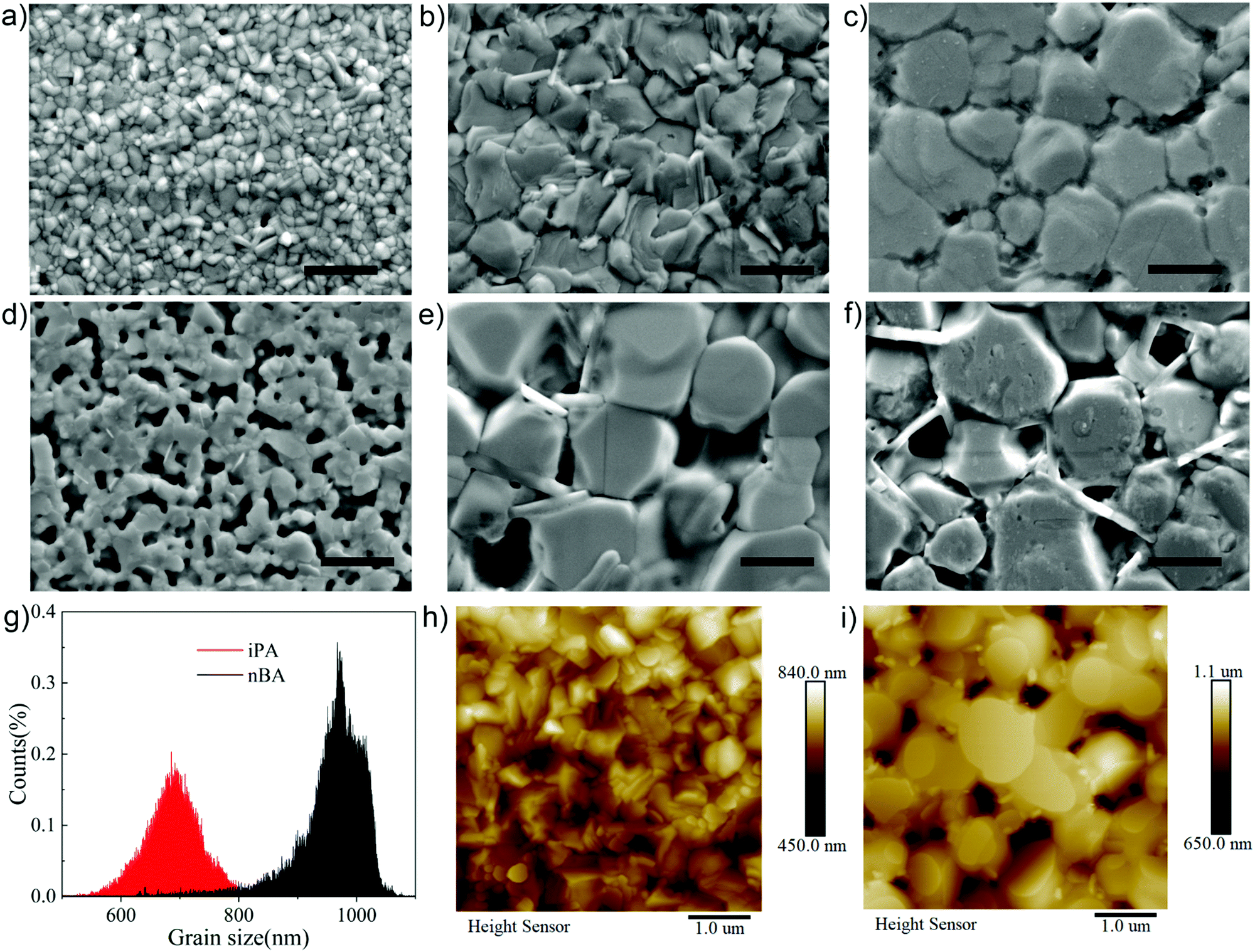 | ||
| Fig. 1 Top-view SEM images of 2D perovskite films prepared using different antisolvents: (a) iPA-unannealed; (b) iPA; (c) nBA; (d) n-propanol; (e) iso-butanol; and (f) sec-butanol; scale bar: 1 μm. (g) Histograms of the measured (AFM) apparent grain size values for iPA and nBA. AFM images (height sensor) of 2D perovskite films prepared using (h) iPA and (i) nBA; scale bar: 1 μm. | ||
When the polarity of the antisolvent is further reduced, the annealed film deposited using toluene, chlorobenzene, or ethyl acetate becomes transparent,46,47 as shown in Fig. S1 and S2 (ESI†). This is because the film is full of large-sized holes. We believe that the formation of the initial nucleus after antisolvent washing is essential for the formation of FA based perovskite films,47 as described below. When the antisolvent used is isopropanol, a fully covered quasi-2D perovskite film is obtained, as shown in Fig. 1b. Similarly, the vertically oriented layered structure appears on the surface of the film, accompanied by large grains. These layered structures may be 2D perovskite slabs.48,49 What is more, unlike films with smooth surfaces prepared by the hot-casting method,1 the films in this study have a rich microstructure on the surface, which stems from the rapid crystallization of 2D phases and partial dissolution of the perovskite layer by the alcohol antisolvent.42
We also studied the surface of the fresh (unannealed) 2D perovskite film prepared using isopropanol, which has the best quality. As shown in Fig. 1a, there is already the formation of sharp crystal grains before annealing, despite the apparent grain size being quite small (142 nm). Since isopropanol and n-butanol produce 2D perovskite films with higher quality, our next discussion will focus on these two antisolvents. 2D perovskite films and 2D PSCs prepared using isopropanol and n-butanol are abbreviated as iPA and nBA, respectively. The root-mean-square (RMS) roughness values of iPA and nBA are 35.8 nm and 63.6 nm, and their average apparent grain sizes are 688 nm and 959 nm, respectively, according to the height sensor of the atomic force microscope (AFM), as shown in Fig. 1g–i.
2.2 Phase distribution
We performed photoluminescence (PL) spectral analysis to study the distribution of 2D perovskite phases (different values of n) along the vertical direction of the film. Due to the limited penetration depth (below 100 nm) of exciting light with a wavelength of 470 nm and an incident angle of 45°, the information in the PL spectrum is limited to the incident surface,50 and the PL spectra of 2D perovskite films under front side (the upper surface of the perovskite) excitation and back side (glass side) excitation are usually different.51 As shown in Fig. 2a, the exciton emission peaks of n = 2 and n = 3 phases at 569 nm and 617 nm coexist with the 3D-like phase at 800 nm,52 which indicates that these 2D perovskite films are composed of multiple quantum wells, instead of an identical n-value phase.53 When excited from the front side of the film, the intensity of 2D perovskite peaks is stronger than when excited from the back side. This means that there are more 2D perovskite phases at the front side of the film, which is different from the normal gradient quantum well structure in most reports.12,27,53,54 Surprisingly, the emission peak at 569 nm is absent in iPA when excited from the back side of the film, the intensity of which is the strongest when excited from the front side. This suggests that 2D perovskite phases are intensively distributed at the top of iPA, while the 3D-like phase is separated at the bottom of iPA. In other words, the film of iPA attains a reverse gradient quantum well structure. In addition, compared with nBA (801 nm), the emission peak of the 3D-like phase in iPA is blue-shifted (791 nm) when excited from the front side of the film, and red-shifted (805 nm) when excited from the back side of the film. This again indicates that the composition of the top of iPA is closer to that of the 2D perovskite (low-n-value phases), while the composition of the bottom of iPA is closer to that of the 3D perovskite (high-n-value phases) than that of nBA.2,25 Such a gradient distribution of 2D perovskite phases is beneficial for carrier transport and sunlight utilization.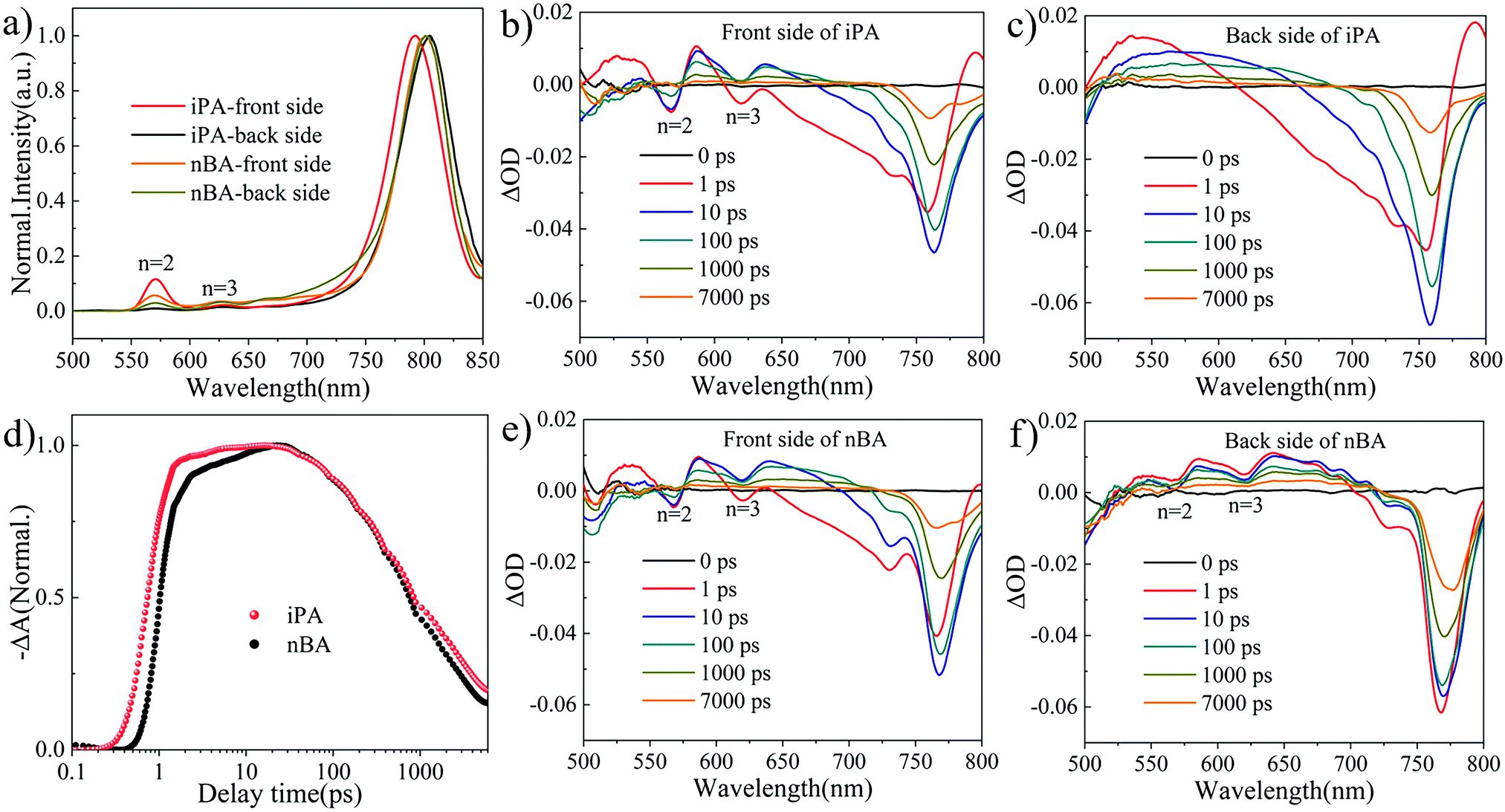 | ||
| Fig. 2 (a) PL spectra of iPA and nBA under front side excitation and back side excitation. Representative TA spectra of iPA and nBA under (b and e) front side excitation and (c and f) back side excitation. (d) The photoexcitation carrier transport kinetics of the 3D-like phase in iPA and nBA under front side excitation. | ||
In addition, in the PL spectra of iPA and nBA, the PL peak of the n = 2 phase is dominant among different low-n-value phases. In order to study this phenomenon, we prepared another quasi-2D perovskite film with more spacer cations (n = 3) and measured its UV-vis absorption spectrum and PL spectrum. As shown in Fig. S3 (ESI†), the 2D perovskite of n = 2 still dominates the quasi-2D perovskite film. For the TMA-based 2D perovskites, the n = 2 phase may be the preferred phase in the growth of quasi-2D perovskite films.3,52
The distribution of n-values is vividly displayed by the confocal laser scanning microscopy (CLSM) photoluminescence (PL) images.26,55 As shown in Fig. S4a and b (ESI†), when the exciting laser is directed at the front side of the films, green grains (with emission wavelengths between 550 nm and 630 nm) derived from low-n-value phases dominate the image. When excited from the back side of the films, as shown in Fig. S4c and d (ESI†), red regions (with emission wavelengths between 650 nm and 700 nm) derived from the 3D-like phase dominate the image. Consistent with the results of the PL spectrum, there are no low-n-value phases at the bottom of iPA. What is more, the size of green regions is smaller in iPA than that in nBA, which is in line with the smaller grain size in the SEM image of iPA. In addition, the relative position of these green regions is similar to the relative position of slabs in the SEM image, which suggests that the slabs in the SEM images are low-n-value 2D perovskites. We further reconstructed the 3D image of the phase distribution according to a series of images of confocal planes, and the results are shown in Fig. S4e and f (ESI†). In iPA, green regions (low-n-value phases) are concentrated at the top of the film. In contrast, green regions are mainly distributed at the top and the bottom of nBA.
2D PSCs suffer from carrier transport arising from the low conductivity of low-n-value phases and the insulating nature of spacer cations.56 We employed transient absorption (TA) spectral analysis24,54 to study the carrier transport processes in iPA and nBA. As shown in Fig. 2b and e, the ground state bleaching (GSB) signals at 568 nm and 620 nm belong to the n = 2 and n = 3 phases present in both iPA and nBA, when the excitation light comes from the front side of the film, which is consistent with the results of PL spectroscopy. The GSB signal of low-n-value phases disappears in iPA when excited from the back side, as shown in Fig. 2c and f. The strong GSB signal of the 3D-like phase (blue region) is more distinct in the pseudo-color images of the TA spectra shown in Fig. S5 (ESI†). The attenuation of the GSB signal of low-n-value phases is accompanied by the rise of the 3D-like phase, suggesting that electrons accumulate from low-n-value phases to the 3D-like phase, that is, the carrier funnelling effect.11,54 We extracted the photoexcitation carrier transport kinetics from the TA spectra, shown in Fig. 2d. The GSB signal enhancement of the 3D-like phase in iPA is in front of nBA. Besides, a GSB signal platform is observed in iPA, while nBA shows another stage of growth (after 1 ps). These indicate that the photoelectrons generated in low-n-value phases move to the 3D-like phase faster in iPA than in nBA.24,57
Although the distribution of 2D perovskite phases (different n-values) from optical measurements can reflect the position of the spacer cation (TMA), the fluorescence quenching effect and the carrier transport process can interfere with the analysis results. Thus, we employed the time-of-flight secondary ion mass spectroscopy (ToF-SIMS) to show the distributions of TMA, FA, and MA unambiguously. In order to obtain accurate information on the distribution of organic cations, a “soft” ion beam (Ar-cluster, a gas cluster ion beam) is used as the sputter beam during the measurement,57,58 and the one-dimensional depth profiles are shown in Fig. 3a and b. The two-dimensional images of the depth profile of the corresponding cations are shown in Fig. S6 (ESI†). Both iPA and nBA show high concentration and uniform distribution of FA along the depth direction. Surprisingly, the content of TMA and MA drops promptly in the initial etching stage (100 s out of 900 s, about 40 nm according to the thickness of the perovskite film, shown in Fig. 3c and d). In addition, the concentration of TMA and MA is higher on the top of iPA than that on the top of nBA. This is reasonable considering that the top of iPA accommodates more low-n-value phases than the top of nBA. What is more, the concentration of TMA and MA in nBA increases slightly when the sputtering time is about 800 s, which is consistent with the results of CLSM-PL (low-n-value phases are mainly located at the top and the bottom of the film of nBA). The reason is that more spacer cations are needed to form low-n-value phases than those needed for the 3D-like phase, according to the structure formula of 2D perovskites.25 This indirectly reflects that MA will also be enriched at the bottom of the film to guide the growth of 2D perovskites in nBA. In addition, only a trace of Cl element remains inside the film, as shown in Fig. S7 (ESI†), suggesting that the annealing process has successfully removed the excess additives.59,60
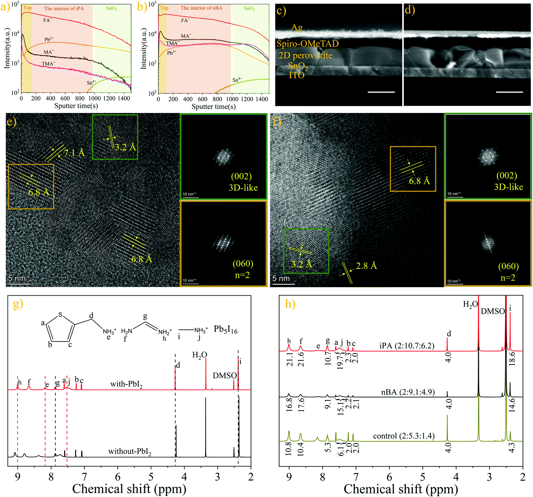 | ||
| Fig. 3 ToF-SIMS depth profiles of (a) iPA and (b) nBA. Cross-sectional SEM images of (c) iPA and (d) nBA; scale bar: 500 nm. HR-TEM images and FFT analysis of (e) iPA and (f) nBA. 1H NMR spectra of the (g) precursor solution with (with-PbI2) or without PbI2 (without-PbI2), (h) iPA, nBA, and the film without the antisolvent washing process (control); the solvent is DMSO-d6. | ||
To understand the accumulation behaviour of MA and TMA at the top of the film, we tested the solubility of these three organic cations in isopropanol and n-butanol. Isopropanol or n-butanol as the antisolvent was added dropwise into a solution (300 μL, 1 M) containing the corresponding organic cation and an equal molar ratio of PbI2 (20 μL of antisolvent per dose to avoid sudden precipitation). The critical volume of antisolvent required to precipitate the solution of MA is twice less than that of FA, as shown in Table S2 (ESI†). More precipitate is obtained when precipitating the solution of MA using isopropanol than that using n-butanol, even though the critical volumes of isopropanol and n-butanol are the same, as shown in Fig. S8 (ESI†). These may be the reasons for the higher concentration of MA at the top of the film, especially in iPA.61 However, the solubility of TMA is the highest among these three cations, which seems to contradict the results of ToF-SIMS. As reported, because the crystallization kinetics of 2D perovskites is faster and the crystallization barrier is lower than that of the 3D perovskite, the thermodynamic non-equilibrium process of the antisolvent washing process leads to the mass production of kinetically more favourable 2D perovskites.39,62 In addition, the chemical shift difference of the ammonium protons (–NH3+) of TMA (0.20 ppm) and MA (0.24 ppm) is larger than that of FA (0.08 ppm), when PbI2 is added into the solution, as shown in the 1H NMR spectra of precursor solutions in Fig. 3g. This suggests that TMA and MA interact with PbI2 more preferentially than FA.58,63,64 Hence, TMA- and MA-based perovskites will be generated first in the initial nucleation stage. As a result, the concentrations of MA and TMA at the top of the film are higher than those in the interior of the film, forming a reverse gradient quantum well structure.
We further conducted high-resolution transmission electron microscopy (HR-TEM) and fast Fourier transform (FFT) of the selected area to show the phase separation of 2D perovskites in iPA and nBA.37,49 As shown in Fig. 3e and f, dominant lattice spacing values of 3.2 Å and 6.8 Å coexist in iPA and nBA, corresponding to the (002) plane of the 3D-like phase and the (060) plane of the n = 2 phase, respectively.37 This also means that the film of iPA is mainly composed of the n = 2 phase (with a domain size of 10–30 nm) and 3D-like phase, and the domain size of the n = 2 phase in nBA is larger (30–50 nm). The energy-dispersive spectrometry (EDS) measurement was conducted to show the distribution of sulfur (S) element. Ascribed to the high resolution of TEM-EDS, we can obtain the exact content of sulfur element in a selected area, as shown in Fig. S9 (ESI†). As shown in Fig. S9b and c (ESI†), the M-line of lead (Pb) overlaps with the K-line of S, and we use the L-line of Pb to subtract the K-line of S for calculations, and the results are shown in Table S3 (ESI†). Interestingly, although the amount of perovskite is higher in area#2 than in area#1 (due to the deeper mass thickness contrast of area#2 than area#1), the fraction of S is 0.7% in area#2, while the content of S is 9.2% (atomic ratio) in area#1, which is close to the atomic ratio of S element in the n = 2 phase (10%). The distribution of Pb and S is clearer in the EDS mapping images shown in Fig. S9d–f (ESI†). This phenomenon indicates that the spacer cations mainly exist in the form of the n = 2 phase, and they are concentrated rather than uniformly distributed in the film, which is consistent with other characterization results.
Next, we studied the accurate compositions of iPA and nBA by 1H NMR spectroscopy,26 and the results are shown in Fig. 3h. Unexpectedly, the ratio of organic cations (TMA:FA:MA) of iPA (2:10.7:6.2) and nBA (2:9.1:4.9) deviates a lot from the feed ratio (2:4:4). To verify the accuracy of the 1H NMR analysis results, we measured the film without the antisolvent washing process and without the annealing process (unannealed). As shown in Fig. S10d (ESI†), the ratio of TMA:FA:MA is 2:4.1:4.0, close to the feed ratio. Then, we checked this ratio in the film without the antisolvent washing process but with annealing, and the obtained ratio is 2:5.3:1.4 (control), as shown in Fig. 3h. In addition, we measured the unannealed films deposited using iPA, nBA, and toluene, respectively, and the results are shown in Fig. S10 and Table S4 (ESI†). These results indicate that a considerable amount of TMA is washed away from the film during the alcoholic solvent washing process.42 Interestingly, more TMA is washed away by iPA (TMA/(TMA + FA + MA) = 10.6%) than nBA (12.5%). This is reasonable considering that the polarity of iPA and nBA is stronger than that of common antisolvents such as toluene, and many TMA spacer cations will be dissolved in these two alcoholic solvents, as shown in Table S2 and Fig. S8 (ESI†). In addition, some TMA cations seem to be lost during the annealing process.46 Nevertheless, the fraction of TMA in our quasi-2D perovskite film is much higher than that of 2D/3D heterojunctions (2.2%),32,65–67 as shown in Fig. S11b (ESI†). What is more, despite using MACl as an additive, many MA cations remain in the films of iPA and nBA. This phenomenon may result from the partial substitution of FA cations by MA cations. As shown in Fig. S10 and Table S4 (ESI†), when the film is washed using iPA or nBA, the ratio of FA to MA (FA/MA) in the film is less than 1, while this ratio is 1 in the precursor or in the film without the antisolvent washing process or the film washed using toluene. This means that the alcoholic solvent washing process will wash away more FA (in the form of FAI or FACl due to the extensive anion exchange) than MA, and MA will serve as component cations (to form the perovskite) to cover the deficiency of A2 cations. In addition, when MACl is directly added into the FAPbI3 precursor solution (FAI:MACl = 2:1),44,58 the perovskite film deposited using isopropanol exhibits a high fraction of MA (FA:MA = 5.4:1) after the annealing process, as shown in Fig. S11a (ESI†).
Next, in order to determine the exact n-value in the film, in addition to the ratio of organic cations obtained from 1H NMR spectroscopy, we also need to know the relative content of organic and inorganic ingredients. X-ray fluorescence (XRF) spectroscopy, a very accurate (1 ppm) characterization technique,68 was performed. As shown in Fig. S12 and Table S4 (ESI†), the relative content of S, Pb, and I (S:Pb:I) in iPA is 2:17.5:55.4, and that in nBA is 2:14.7:46.5. With these data in hand, we can deduce the ratio of different components (TMA:(FA + MA):Pb:I) in the film, which is 2:16.9:17.5:55.4 for iPA and 2:14.0:14.7:46.5 for nBA. Therefore, the average n-value of iPA is about 18 and the average n-value of nBA is about 15. For the first time, we find that the final n-value in the film can be very different from the feed ratio (n-value of 5). However, most of the published work uses the feed ratio to determine the average n-value of the film.9,35 It is better to figure out the actual composition in the film before discussing the relationship between the performance and composition of 2D perovskites.
2.3 Growth process of 2D perovskite films
Next, we try to figure out the function of the antisolvent deposition process and its crystallization kinetics. UV-vis absorption and X-ray diffraction (XRD) testing was performed for the freshly prepared film before annealing. As shown in Fig. 4a and b, both the exciton absorption peak of the n = 2 phase 2D perovskite at 569 nm and the absorption edge of the 3D-like phase already exist on the freshly prepared films, suggesting that there is spontaneous formation of 2D perovskites and the 3D-like perovskite before annealing. All the films have almost the same absorption edge of 1.53 eV, and the dominant low-n-value phase is n = 2. The annealed film shows stronger absorption in the entire spectra than the freshly prepared film, which means that the annealing process enables a higher crystallinity of the annealed films, because the amorphous solvate precursors have been completely converted to 2D perovskites.69,70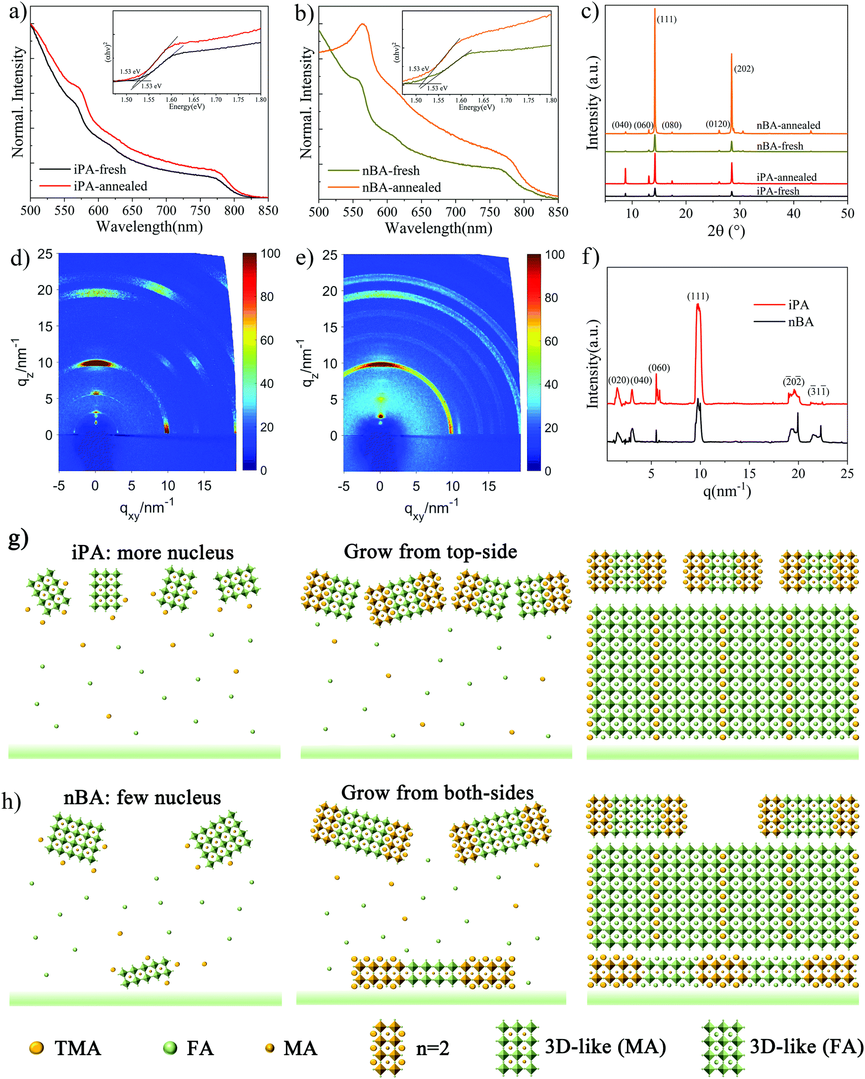 | ||
| Fig. 4 UV-vis absorption spectra of (a) iPA and (b) nBA before (iPA-fresh and nBA-fresh) and after annealing (iPA-annealed and nBA-annealed). (c) XRD patterns of iPA and nBA before and after annealing. GIWAXS patterns of (d) iPA and (e) nBA, and (f) the 1D-GIWAXS profiles along the out-of-plane direction (qz). Schematic diagrams of the film formation process of (g) iPA and (h) nBA. | ||
Then, we checked the XRD patterns of these films to determine whether there is formation of intermediate phases, and the results are shown in Fig. 4c. The diffraction angles (2θ) of 14.20° and 28.46° are indexed to the (111) and (202) crystal planes of the perovskite, respectively,31,32,71 2θ values of 8.75° and 13.06° are assigned to the (040) and (060) planes of the n = 2 phase 2D perovskite, respectively,32,72 and no diffraction peaks belonging to the intermediate phases are observed. This is different from our previous work concerning the hot-casting method, in which no signals can be observed at low diffraction angles (2θ < 10°) and low-n-value phases are located at the bottom of the films (normal gradient quantum well structure).25 This means that the n-value distribution of the film prepared by the anti-solvent method is different from that prepared using the hot casting method, as we discussed above. Moreover, 2D perovskites, n = 2 phase specifically, have already been formed in freshly prepared films, which is consistent with the result of the UV-vis absorption spectrum. After annealing, the intensity of the diffraction peaks increased, and the full width at half-maximum (FWHM) value decreased, indicating that the grain size increased significantly (from 142 nm to 680 nm). What is more, the intensity of 2θ = 8.75° in iPA is stronger than that in nBA, which may be caused by the higher concentration of the n = 2 phase at the top of iPA.
We conducted the grazing incidence wide-angle X-ray scattering (GIWAXS) measurement to show the orientation of 2D perovskite phases. As shown in Fig. 4d and e, the GIWAXS pattern of iPA is composed of distinct Bragg spots, which is different from that of nBA composed of Bragg rings, suggesting that iPA has a preferred orientation. Along the qz direction, Bragg spots at qz = 1.6 nm−1, 3.0 nm−1, and 5.5 nm−1 are indexed to the (020), (040), and (060) facets of the n = 2 phase, respectively.26,72 To compare the diffraction intensity of these Bragg spots, we extracted the line-cut profile curves of iPA and nBA along the out-of-plane direction (qz), as shown in Fig. 4f. Interestingly, contradictory to the results of XRD patterns, the intensity of the (111) peak (qz = 9.9 nm−1) in iPA is stronger than that in nBA. This may result from the preferred out-of-plane orientation of the (111) facet in iPA.73 The intensive distribution of 2D perovskites at the top of the film can template the directional growth of the subsequent perovskite film.74 In addition, due to the limited penetration depth of the X-ray (0.124 nm) with an incident angle of 0.16°, the information in the GIWAXS patterns comes from the top of the film (less than 20 nm).75 The presence of 2D perovskite signals in the GIWAXS patterns confirms again that the top of the film is rich in low n-value phases.
Based on the above facts, we proposed a crystallization process of the film prepared by the alcoholic antisolvent deposition method. The nucleation stage: When the wet film is extracted using an alcoholic solvent, a MA-based crystal nucleus forms immediately at the top of the film (ToF-SIMS) for its low solubility and strong interaction with PbI2, as shown in Table S2 (ESI†) and Fig. 3g. What is more, when we prepared a quasi-2D perovskite film from the precursor solution of TMAI:MAI:PbI2:MACl = 2:4:5:4 (iPA-MA), the reverse gradient quantum well structure is lost, as shown in Fig. S13 (ESI†). Although the number of 2D perovskites on the top of the film is still larger than that at the bottom of the film, there are clear 2D perovskite signals at the bottom of the film. Therefore, the accumulation of MA cations at the top of the film is a precondition for the formation of the reverse gradient quantum well structure in this study.76
The growth stage: TMA-based 2D perovskites adhere to the MA-based crystal nucleus to nucleate and grow due to its rapid crystallization rate, and the schematic diagrams are shown in Fig. 4g and h. The TMA-based 2D perovskites and MA-based 3D-like perovskites serve as a template to direct the growth of perovskites.74,77 Due to the strong polarity of iPA, large-sized crystal nuclei are dissolved, and many small-sized crystal nuclei form instead. As a result, the heterogeneous nucleation at the bottom of iPA can be ignored, but not in nBA. Meanwhile, as shown in Fig. 1, the grain size of the film produced by iPA is much smaller than that of nBA and other less polar antisolvents. The final stage: According to the results of transient absorption (TA) spectra, PL spectra, and UV-vis absorption spectra, our 2D perovskite films are mainly composed of 2D phases with n-values of 2 and 3 (n = 2 and n = 3) and the 3D-like phase (n ≥ 10). Considering that the number of spacer cations required to construct low-n-value phases is much higher than that for high-n-value phases, the formation of n = 2 and n = 3 phases on the top of the film will consume a large amount of TMA spacer cations. As a result, the rest of the quasi-2D perovskites in the film are mainly 3D-like phase. Compared with nBA, the higher nucleus density of iPA induces more TMA to participate in the formation of the 2D perovskite at the top of the film. In contrast, as shown in Fig. 4h, since only a small number of TMA cations are consumed on the top of nBA, a considerable number of TMA cations will form the 2D perovskite in the interior of the film, especially at the interface between the substrate and the perovskite layer (heterogeneous nucleation).53 What is more, the total number of TMA spacer cations remained in nBA is larger than that in iPA, after the alcoholic antisolvent washing process, as demonstrated by the 1H NMR analysis. As a result, low-n-value phases can be observed on the top and at the bottom of nBA, while these low-n-value phases can be observed only at the top of iPA. This is consistent with the results of CLSM-PL shown in Fig. S4 (ESI†). The distribution of quantum wells is sandwich-like in nBA, while it is reversely graded in iPA. Only a small number of TMA cations remain in iPA, which means that the photoelectric properties of the 3D-like phase in iPA are very close to those of the 3D perovskite, which is conducive to the efficiency of PSCs.
2.4 Photovoltaic performance and stability
For the reverse gradient quantum well structure of the film, we examined their photovoltaic performance with a normal device structure, that is, ITO/SnO2/perovskite/Spiro-OMeTAD/Ag. The perovskite layer is obtained by a one-step deposition method using iPA and nBA, respectively. The cross-sectional SEM images of the devices are shown in Fig. 3c and d. The film of iPA has large and vertically oriented crystal grains that extends throughout the entire film, and the average thickness of the film is 330 nm. However, holes and obvious defects are found in nBA, and the crystal grains are double-layered, which may be caused by the secondary nucleation at the film bottom.78 From the current density–voltage (J–V) curves shown in Fig. 5a, the photovoltaic performance of iPA is much higher than that of nBA. The highest PCE of iPA is 20.12% in the reverse scan, with an open circuit voltage (Voc) of 1.15 V, a short-circuit current density (Jsc) of 22.15 mA cm−2, and a fill factor (FF) of 0.79. This is the highest PCE in the field of 2D PSCs (Table S9, ESI†). However, these photovoltaic parameters are poor in nBA, especially the Voc drops to 1.05 V in the reverse scan, and even 1.01 V in the front scan, as summarized in Table S5 (ESI†). Such a low Voc may be caused by the high trap density and the presence of holes in nBA.13,28 The lower Jsc and FF in nBA than those in iPA may be caused by the disordered transport of carriers, arising from the sandwich-like distribution of quantum wells. To further demonstrate the directional transport characteristic of charge carriers along the gradient of n-values, we tested the photovoltaic performance of iPA on an inverted device structure, and the results are shown in Fig. S14 (ESI†). The Voc of the devices drops below 0.90 V, regardless of whether it is a PEDOT:PSS substrate or a nickel oxide (NiOx) substrate. This result suggests that photogenerated holes are directionally transported to low-n-value phases located at the top of iPA, and the normal device structure is essential for iPA with a reverse gradient quantum well structure.54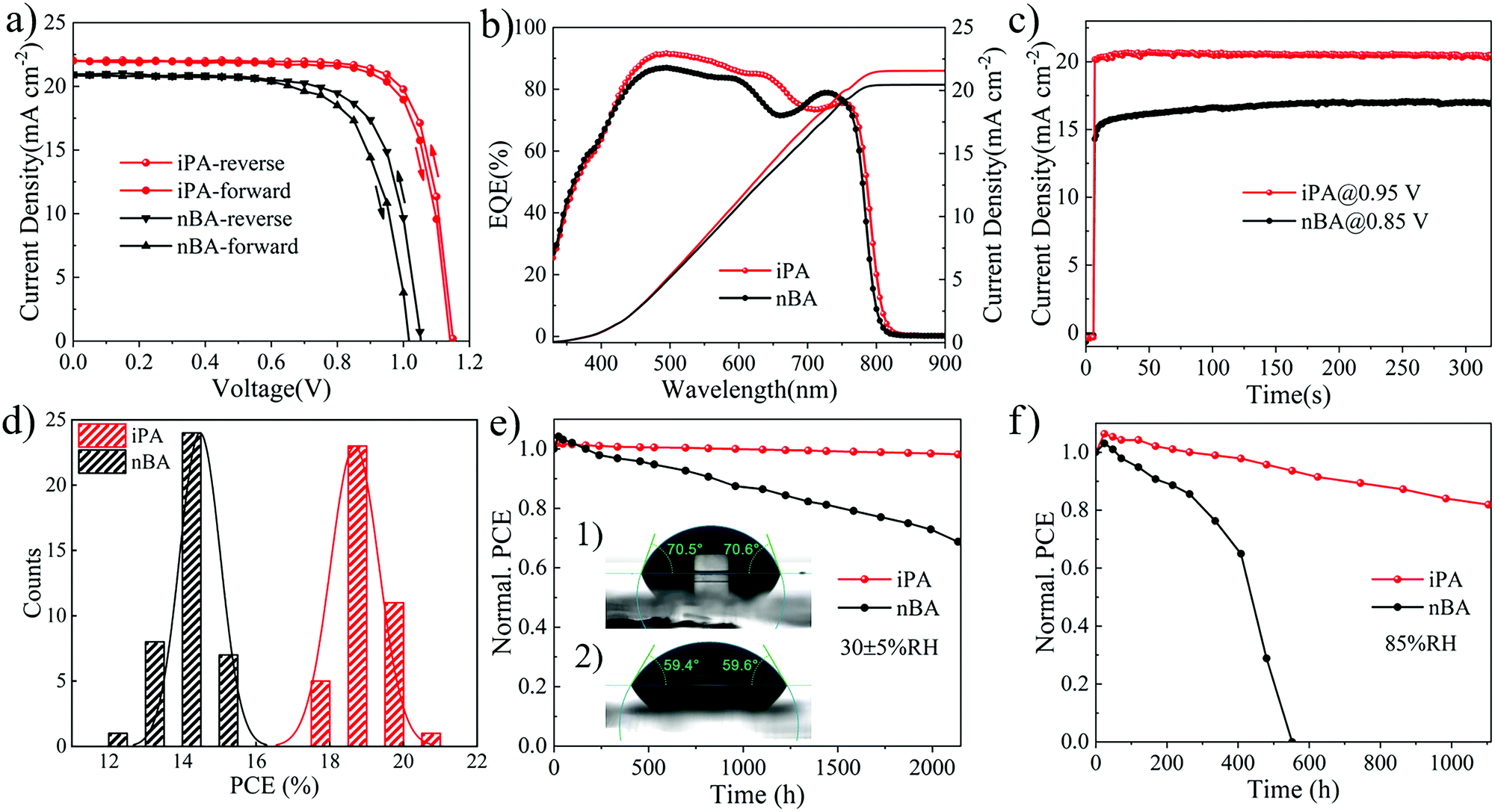 | ||
| Fig. 5 (a) J–V curves under forward and reverse scans, (b) EQE spectra and integrated current density curves, (c) stabilized photocurrent output of the champion devices, (d) histogram distribution of PCE, and the humidity stability of iPA and nBA in a dark environment with (e) 30 ± 5% RH and (f) 85% RH. | ||
The hysteresis is weak and the Jsc value matches well with the results of external quantum efficiency (EQE) spectroscopy, as shown in Fig. 5b. The EQE value reaches 90% in the range of 500–600 nm in iPA, suggesting its extraordinary photon-to-electron conversion capability. Meanwhile, the EQE value at a wavelength over 650 nm is much higher than that of our previous 2D PSCs prepared by the hot-casting method.25 The bandgap derived from the EQE spectrum of iPA is 1.53 eV, which is smaller than the bandgap of 1.59 eV for the MA-based 2D perovskite.25 Thus, the photocurrent of the FA-based 2D PSCs is higher than that reported in our previous work (Jsc = 17.50 mA cm−2).25 To show the steady-state power output ability, we measured the photocurrent at a fixed voltage (maximum power point), and the results are shown in Fig. 5c. After continuous illumination for 300 s, the stabilized PCE of iPA is 19.44% with an output current density of 20.46 mA cm−2 at 0.95 V. This is higher than that of nBA with a stabilized PCE of 14.4% and an output current density of 16.94 mA cm−2 at 0.85 V. The reproducibility is shown in Fig. 5d and Fig. S15 (ESI†). After calculating the photovoltaic parameters of 40 devices, the average PCE of iPA is 18.81 ± 0.65% and the average PCE of nBA is 14.39 ± 0.55.
To show the universality of the isopropanol washing method, we tested the performance of devices with different kinds of spacer cations, and the results are shown in Table S6 (ESI†). The photovoltaic performance of thiophene-based spacer cations is much higher than that of aliphatic-based and aromatic-based spacer cations, and there is not much difference between TMA and 3TMA. The solubility of spacer cations in isopropanol, the formation energy of corresponding 2D perovskites, and the dielectric constant of spacer cations comprehensively determine the performance of the device.2,11,79 Our next work will focus on uncovering the internal mechanism of the excellent photovoltaic performance of thiophene-based spacer cations.
To assess the stability of our quasi-2D PSCs, we evaluated the hydrophobicity of quasi-2D perovskite films’ surface firstly. The static water contact angle of iPA is 70.5°, which is larger than that of nBA (59.5°), as shown in the inset of Fig. 5e. As expected, the bulky hydrophobic spacer cations (TMA) located at the top of the film can efficiently suppress the penetration of water molecules into the interior of the perovskite film. Then, the films of iPA and nBA are directly exposed to 85% RH for 360 h for the humidity aging test. From the UV-vis absorption spectra, as shown in Fig. S16 (ESI†), the absorption of nBA above the wavelength of 600 nm is significantly reduced, while the exciton absorption peak at 569 nm belonging to the n = 2 phase is still very strong. This indicates that the 3D-like phase in the film has been decomposed, leaving only the low-n-value 2D perovskite phases with higher humidity stability.80 The XRD analysis confirmed this phenomenon again. As shown in Fig. S17 (ESI†), the aged film of nBA shows many peaks at low diffraction angles (2θ < 10°), which are attributed to the low-n-value 2D perovskite phases. Next, we measured the shelf-life of devices under various conditions, wherein the unstable Spiro-OMeTAD layer and Ag electrode were substituted with PTAA and Au, respectively. When the unencapsulated devices are stored in an electronic drying cabinet with 30 ± 5% RH, the PCE of iPA retains 98% of the initial value after 2000 h, while that of nBA is 68%. We tested the humidity stability of the devices under a harsher environment (85% RH), and the results are shown in Fig. 5f. The PCE of iPA degrades to 93% after 530 h and 77% after 1000 h, while the PCE of nBA swiftly drops to 0% after aging for 530 h. Such poor humidity stability of nBA may be caused by the defects and holes in the film, which are the staring points of the decomposition.28 Compared to our previous work, the humidity stability of iPA is even higher, despite its 2D phases being fewer. This suggests that the reverse gradient quantum well structure is better when considering the humidity stability of the devices. In our previous work, the PCE of the device (normal gradient quantum well structure) degrades to 83% after 1510 h under 30 ± 5% RH, and 67% after 530 h under 85% RH.25
To estimate the thermal stability of the devices, the unencapsulated devices are heated at 85 °C on a hot plate in a N2 filled glove box. After a certain interval, the J–V curves of these devices were measured and are shown in Fig. S18 (ESI†). The PCE of iPA retains 88% of the initial value after thermal aging for 360 h, whereas that of nBA is 74%. In contrast, the PCE of iPA-MA degrades to 43% after 360 h. The bare films of iPA and iPA-MA are aged under the same conditions for the XRD measurement. As shown in Fig. S19 (ESI†), the film of iPA-MA shows a very strong diffraction peak belonging to PbI2, suggesting that MA gradually volatilizes during the thermal aging process. However, there is no obvious change in the XRD pattern of iPA.
We further measured the long-term operational stability (at a bias of 0.95 V) of iPA under full solar illumination. After continuous operation at the maximum power point for 360 h, the device of iPA retains 96% of its initial efficiency, as shown in Fig. S20 (ESI†). The rise of PCE during the first 24 h may have originated from the light and thermally induced trap passivation process.3
2.5 Carrier transport properties
Then, we measured the time-resolved PL (TRPL) decay of iPA and nBA to evaluate the behavior of charge carriers. As shown in Fig. 6a, the exponential regions of the TRPL decay curves of neat perovskite films (iPA and nBA) are well fitted by the mono-exponential function.81,82 The carrier lifetime of iPA is 936 ns, which is longer than that of nBA (570 ns). What is more, we measured the external photoluminescence quantum efficiencies (PLQEs) of iPA and nBA. As shown in Fig. S21 (ESI†), the PLQE of iPA (5.7%) is significantly higher than that of nBA (0.62%). These mean that the trap-induced non-radiative recombination in iPA is significantly suppressed compared with nBA under the same excitation conditions.83,84 The fluence-dependent TRPL decays are shown in Fig. S22 (ESI†). The fast initial decay of nBA at low fluences may result from the high density of surface defects.85 The abundant surface defects of nBA are evident in the fluence-dependent TRPL decay of SnO2/nBA/Spiro, as shown in Fig. S22d (ESI†). There is a dominant fast initial decay at delay time <10 ns, which arises from the loss of carriers during the charge extraction process.82 In addition, the TRPL decay curves of SnO2/nBA/Spiro overlap with each other at different fluences, which is different from SnO2/iPA/Spiro in Fig. S22c (ESI†). We attribute this phenomenon to the fact that the interface between nBA and Spiro-OMeTAD is full of defects, which dominate the TRPL decay and make it insensitive to fluence.86 The second TRPL decays of SnO2/iPA/Spiro and SnO2/nBA/Spiro originating from the interface recombination are mono-exponentially fitted.82 The results are shown in Fig. 6a. The longer carrier lifetime in SnO2/iPA/Spiro is consistent with its stronger relative steady-state PL intensity,87 which is shown in Fig. S23 (ESI†). These facts mean that the bulk and surface defect density values in iPA are much lower than those in nBA, which are the internal causes of the higher Voc of iPA.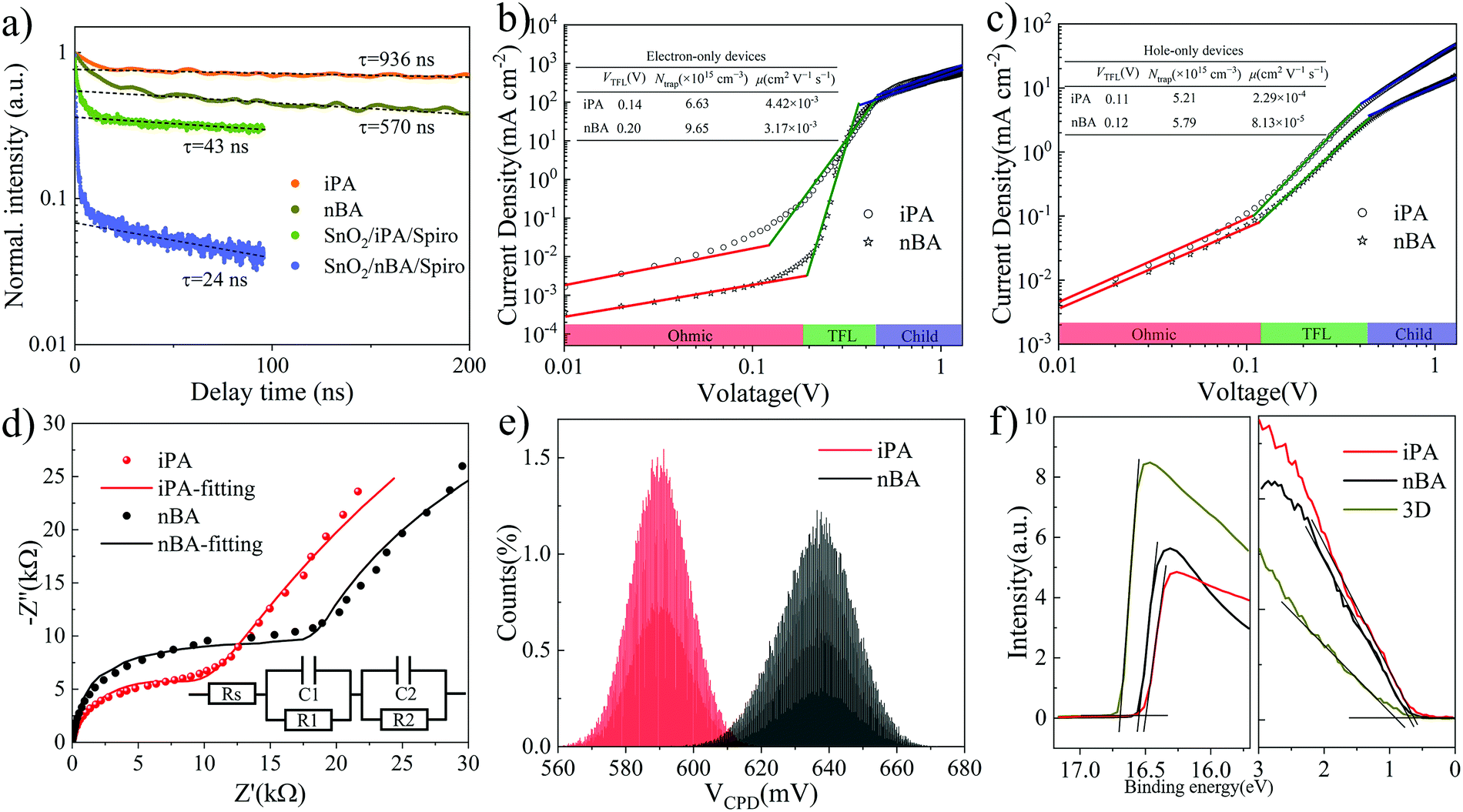 | ||
| Fig. 6 (a) TRPL decays of iPA, nBA, SnO2/iPA/Spiro, and SnO2/nBA/Spiro. The films are excited at 470 nm (40 nJ cm−2) through the top surface side. The dashed lines are extrapolated fits to the mono-exponential tail of TRPL decays at a fluence of 40 nJ cm−2, from which the PL decay time values are obtained. Dark J–V curves of (b) electron-only devices and (c) hole-only devices and the corresponding fitting parameters in the inset. (d) Nyquist plots and the fitting curves of iPA and nBA measured in a dark environment and the equivalent-circuit model in the inset. (e) Histograms of the measured CPD values for iPA and nBA. (f) UPS spectra of secondary electron cut-off and valence bands of iPA, nBA, and the 3D perovskite film. | ||
To assess the density of traps (Ntrap) and the carrier mobility of electrons (μe) and holes (μh), we measured the dark J–V curves of electron-only devices and hole-only devices. The electron-only devices take a structure of ITO/SnO2/2D perovskite/PCBM/Ag and the hole-only devices take a structure of ITO/PEDOT:PSS/2D perovskite/Spiro-OMeTAD/Ag, where the 2D perovskite layer is iPA or nBA. As shown in Fig. 6b and c, the J–V curves change from the linear region (ohmic region) at low voltages to the trap-filled limit region, which finally reaches the space-charge-limited current (SCLC) region.28,29 The Ntrap is evaluated by the onset voltage of the trap-filled limit region (VTFL), and the carrier mobility is derived from the SCLC region.13 The detailed calculation process is shown in the Experimental part, and the results are summarized in the inset in Fig. 6b and c. It is worth noting that the relative electrical permittivity of iPA and nBA was measured by EIS,88,89 as shown in Fig. S24 (ESI†). The Ntrap values of electrons and holes in iPA are lower than those in nBA. The lowest Ntrap of 5.21 × 1015 cm−3 is obtained for the hole-only device of iPA. The carrier mobility of iPA is higher than that of nBA as well. Among them, the hole mobility increased most obviously, from 8.13 × 10⁻⁵ cm2 V−1 s−1 of nBA to 2.29 × 10⁻⁴ cm2 V−1 s−1 of iPA. The fewer trap density and higher carrier mobility of iPA endow the device with better photovoltaic performance.28
To further study the relationship between the charge carrier dynamics and the photovoltaic performance. The transient photovoltage (TPV, under open-circuit conditions) and transient photocurrent (TPC, under short-circuit conditions) measurements are conducted to evaluate the recombination time (lifetime of carriers) and transport (extraction) time of photocarriers, respectively.2,13,28 From the photovoltage decay curves in Fig. S25a (ESI†), the carrier lifetime of iPA is 131.1 μs, which is longer than that of nBA (27.4 μs). This suggests that the trap density is reduced, and the trap-induced nonradiative recombination is suppressed in iPA, which is consistent with the enlarged Voc of iPA. The same results can be found in their electrochemical impedance spectra (EIS). As shown in Fig. 6d and Table S7 (ESI†), the carrier recombination resistance is larger in iPA than that in nBA.90 Like the TPV analysis, we obtained the charge carrier extraction times for iPA (0.93 μs) and nBA (1.91 μs) from the photocurrent decay curves in Fig. S25b (ESI†) under the mono-exponential decay model. The elongated carrier lifetime and the shortened carrier extraction time of iPA may come from its reverse gradient quantum well structure, which enables the directional transport of carriers in the film. In contrast, the sandwich-like distribution of quantum wells in nBA disrupts the carrier transport process.
The average contact potential difference (CPD) values of iPA and nBA are determined to be 0.59 V and 0.64 V, respectively, from Kelvin probe force microscopy (KPFM) measurements, as shown in Fig. 6e and Fig. S26 (ESI†). A lower average CPD means a larger work function (downward shifted Fermi level),32 which suggests that the surface compositions of iPA and nBA are different. We conducted the ultraviolet photoemission spectroscopy (UPS) of iPA and nBA to study the energy band alignment. As shown in Fig. 6f and Table S8 (ESI†), compared with the Fermi level (EF) of the 3D perovskite (−4.53 eV) and nBA (−4.68 eV), the EF of iPA is shifted downward to −4.73 eV. This is consistent with the results of KPFM and perhaps the enrichment of low-n-value phases at the top of iPA makes the EF of iPA deeper. Besides, differing from the n-type character of the 3D perovskite, iPA and nBA are p-type. Since the interior of iPA is composed of the 3D-like phase (n-type), the naturally formed p–n junction in iPA facilitates the directional transport of charge carriers.91 Combining the results of UPS and the optical absorption edge, the energy band alignment is obtained, as shown in Fig. S27 (ESI†). Just like researchers passivated the surface of the 3D perovskite by a thin layer of 2D perovskite, the shallower conduction band and the deeper EF of iPA can efficiently block the backflow of electrons and facilitate the extraction of holes by the hole transport layer.31,32,92
3. Conclusions
A high-quality FA-MA mixed 2D perovskite film is obtained by isopropanol washing. Low-n-value phases are concentrated at the top of the film, while 3D-like perovskite phases are enriched inside the film, forming a reverse gradient quantum well structure. The isopropanol washing process removes half of the spacer cations (TMA) from the film, and the final average n-value in the film is 18. The quantum confinement effect inside the film is significantly weakened, and the external quantum efficiency response wavelength is extended to 812 nm. Besides, the film shows out-of-plane oriented grains, downward-shifted Fermi levels, reduced trap density, and extended carrier lifetime. A record PCE of 20.12% is achieved on a normal device structure. The PCE of the unencapsulated device retains 98% of its initial value after aging at 30 ± 5% RH for 2000 h and retains 96% after continuous operation at the maximum power point for 360 h. We believe that further weakening the quantum confinement effect and fine-tuning the distribution of quantum wells is the future of quasi-2D PSCs.Conflicts of interest
There are no conflicts to declare.Acknowledgements
This study was funded partly by the National Natural Science Foundation of China (Grant No. 51950410581), Shanghai Government (20JC141500), and the Open Fund of Zhejiang Tsinghua Institute of Flexible Electronics Technology. The authors thank the support from staff at beamline BL14B in the Shanghai Synchrotron Radiation Facility (SSRF) for the GIWAXS measurement. We acknowledge the Instrumental Analysis Center of Shanghai Jiao Tong University for PLQE, AFM, ToF-SIMS, UPS, and TEM analyses.References
- H. Tsai, W. Nie, J. C. Blancon, C. C. Stoumpos, R. Asadpour, B. Harutyunyan, A. J. Neukirch, R. Verduzco, J. J. Crochet, S. Tretiak, L. Pedesseau, J. Even, M. A. Alam, G. Gupta, J. Lou, P. M. Ajayan, M. J. Bedzyk and M. G. Kanatzidis, Nature, 2016, 536, 312–316 CrossRef CAS.
- G. Wu, X. Li, J. Zhou, J. Zhang, X. Zhang, X. Leng, P. Wang, M. Chen, D. Zhang, K. Zhao, S. Liu, H. Zhou and Y. Zhang, Adv. Mater., 2019, 31, 1903889 CrossRef CAS.
- X. Lian, H. Wu, L. Zuo, G. Zhou, X. Wen, Y. Zhang, G. Wu, Z. Xie, H. Zhu and H. Chen, Adv. Funct. Mater., 2020, 30, 2004188 CrossRef CAS.
- N. J. Jeon, J. H. Noh, Y. C. Kim, W. S. Yang, S. Ryu and S. I. Seok, Nat. Mater., 2014, 13, 897–903 CrossRef CAS.
- B. Febriansyah, Y. Lekina, J. Kaur, T. J. N. Hooper, P. C. Harikesh, T. Salim, M. H. Lim, T. M. Koh, S. Chakraborty, Z. X. Shen, N. Mathews and J. England, ACS Nano, 2021, 15, 6395–6409 CrossRef CAS.
- L. Mao, P. Guo, M. Kepenekian, I. Spanopoulos, Y. He, C. Katan, J. Even, R. D. Schaller, R. Seshadri, C. C. Stoumpos and M. G. Kanatzidis, J. Am. Chem. Soc., 2020, 142, 8342–8351 CrossRef CAS.
- J. Qing, X.-K. Liu, M. Li, F. Liu, Z. Yuan, E. Tiukalova, Z. Yan, M. Duchamp, S. Chen, Y. Wang, S. Bai, J.-M. Liu, H. J. Snaith, C.-S. Lee, T. C. Sum and F. Gao, Adv. Energy Mater., 2018, 8, 1800185 CrossRef.
- F. Zhang, D. H. Kim, H. Lu, J. S. Park, B. W. Larson, J. Hu, L. Gao, C. Xiao, O. G. Reid, X. Chen, Q. Zhao, P. F. Ndione, J. J. Berry, W. You, A. Walsh, M. C. Beard and K. Zhu, J. Am. Chem. Soc., 2019, 141, 5972–5979 CrossRef CAS PubMed.
- H. Ren, S. Yu, L. Chao, Y. Xia, Y. Sun, S. Zuo, F. Li, T. Niu, Y. Yang, H. Ju, B. Li, H. Du, X. Gao, J. Zhang, J. Wang, L. Zhang, Y. Chen and W. Huang, Nat. Photonics, 2020, 14, 154–163 CrossRef CAS.
- X. Zhao, T. Liu, A. B. Kaplan, C. Yao and Y.-L. Loo, Nano Lett., 2020, 20, 8880–8889 CrossRef CAS PubMed.
- G. Wu, T. Yang, X. Li, N. Ahmad, X. Zhang, S. Yue, J. Zhou, Y. Li, H. Wang, X. Shi, S. Liu, K. Zhao, H. Zhou and Y. Zhang, Matter, 2021, 4, 582–599 CrossRef CAS.
- R. Yang, R. Li, Y. Cao, Y. Wei, Y. Miao, W. L. Tan, X. Jiao, H. Chen, L. Zhang, Q. Chen, H. Zhang, W. Zou, Y. Wang, M. Yang, C. Yi, N. Wang, F. Gao, C. R. McNeill, T. Qin, J. Wang and W. Huang, Adv. Mater., 2018, 30, 1804771 CrossRef PubMed.
- A. A. Sutanto, N. Drigo, V. I. E. Queloz, I. Garcia-Benito, A. R. Kirmani, L. J. Richter, P. A. Schouwink, K. T. Cho, S. Paek, M. K. Nazeeruddin and G. Grancini, J. Mater. Chem. A, 2020, 8, 2343–2348 RSC.
- J. Zhang, J. Qin, M. Wang, Y. Bai, H. Zou, J. K. Keum, R. Tao, H. Xu, H. Yu, S. Haacke and B. Hu, Joule, 2019, 3, 3061–3071 CrossRef CAS.
- B. Kim and S. I. Seok, Energy Environ. Sci., 2020, 13, 805–820 RSC.
- P. Liu, N. Han, W. Wang, R. Ran, W. Zhou and Z. Shao, Adv. Mater., 2021, 33, 2002582 CrossRef CAS.
- D. H. Cao, C. C. Stoumpos, O. K. Farha, J. T. Hupp and M. G. Kanatzidis, J. Am. Chem. Soc., 2015, 137, 7843–7850 CrossRef CAS.
- Y. Lin, Y. Fang, J. Zhao, Y. Shao, S. J. Stuard, M. M. Nahid, H. Ade, Q. Wang, J. E. Shield, N. Zhou, A. M. Moran and J. Huang, Nat. Commun., 2019, 10, 1008 CrossRef PubMed.
- I. C. Smith, E. T. Hoke, D. Solis-Ibarra, M. D. McGehee and H. I. Karunadasa, Angew. Chem., Int. Ed., 2014, 53, 11232–11235 CrossRef CAS.
- J.-C. Blancon, H. Tsai, W. Nie, C. C. Stoumpos, L. Pedesseau, C. Katan, M. Kepenekian, C. M. M. Soe, K. Appavoo, M. Y. Sfeir, S. Tretiak, P. M. Ajayan, M. G. Kanatzidis, J. Even, J. J. Crochet and A. D. Mohite, Science, 2017, 355, 1288–1292 CrossRef CAS PubMed.
- G. Grancini and M. K. Nazeeruddin, Nat. Rev. Mater., 2018, 4, 4–22 CrossRef.
- L. Mao, C. C. Stoumpos and M. G. Kanatzidis, J. Am. Chem. Soc., 2019, 141, 1171–1190 CrossRef CAS.
- C. Liang, H. Gu, Y. Xia, Z. Wang, X. Liu, J. Xia, S. Zuo, Y. Hu, X. Gao, W. Hui, L. Chao, T. Niu, M. Fang, H. Lu, H. Dong, H. Yu, S. Chen, X. Ran, L. Song, B. Li, J. Zhang, Y. Peng, G. Shao, J. Wang, Y. Chen, G. Xing and W. Huang, Nat. Energy, 2021, 6, 38–45 CrossRef CAS.
- Z. Xu, D. Lu, F. Liu, H. Lai, X. Wan, X. Zhang, Y. Liu and Y. Chen, ACS Nano, 2020, 14, 4871–4881 CrossRef CAS PubMed.
- J. Liang, Z. Zhang, Y. Zheng, X. Wu, J. Wang, Z. Zhou, Y. Yang, Y. Huang, Z. Chen and C.-C. Chen, J. Mater. Chem. A, 2021, 9, 11741–11752 RSC.
- S. Shao, H. Duim, Q. Wang, B. Xu, J. Dong, S. Adjokatse, G. R. Blake, L. Protesescu, G. Portale, J. Hou, M. Saba and M. A. Loi, ACS Energy Lett., 2019, 5, 39–46 CrossRef.
- L. Kuai, J. Li, Y. Li, Y. Wang, P. Li, Y. Qin, T. Song, Y. Yang, Z. Chen, X. Gao and B. Sun, ACS Energy Lett., 2019, 5, 8–16 CrossRef.
- Y. Yang, C. Liu, O. A. Syzgantseva, M. A. Syzgantseva, S. Ma, Y. Ding, M. Cai, X. Liu, S. Dai and M. K. Nazeeruddin, Adv. Energy Mater., 2021, 11, 2002966 CrossRef CAS.
- Y. Yang, C. Liu, A. Mahata, M. Li, C. Roldán-Carmona, Y. Ding, Z. Arain, W. Xu, Y. Yang, P. A. Schouwink, A. Züttel, F. De Angelis, S. Dai and M. K. Nazeeruddin, Energy Environ. Sci., 2020, 13, 3093–3101 RSC.
- E. Ruggeri, M. Anaya, K. Gałkowski, G. Delport, F. U. Kosasih, A. Abfalterer, S. Mackowski, C. Ducati and S. D. Stranks, Adv. Mater., 2019, 31, 1905247 CrossRef CAS PubMed.
- Y. Qiu, J. Liang, Z. Zhang, Z. Deng, H. Xu, M. He, J. Wang, Y. Yang, L. Kong and C.-C. Chen, J. Phys. Chem. C, 2021, 125, 1256–1268 CrossRef CAS.
- M. He, J. Liang, Z. Zhang, Y. Qiu, Z. Deng, H. Xu, J. Wang, Y. Yang, Z. Chen and C.-C. Chen, J. Mater. Chem. A, 2020, 8, 25831–25841 RSC.
- H. Kim, M. Pei, Y. Lee, A. A. Sutanto, S. Paek, V. I. E. Queloz, A. J. Huckaba, K. T. Cho, H. J. Yun, H. Yang and M. K. Nazeeruddin, Adv. Funct. Mater., 2020, 30, 1910620 CrossRef CAS.
- Y.-W. Jang, S. Lee, K. M. Yeom, K. Jeong, K. Choi, M. Choi and J. H. Noh, Nat. Energy, 2021, 6, 63–71 CrossRef CAS.
- D. Li, Z. Xing, L. Huang, X. Meng, X. Hu, T. Hu and Y. Chen, Adv. Mater., 2021, 33, 2101823 CrossRef CAS.
- H. Lai, B. Kan, T. Liu, N. Zheng, Z. Xie, T. Zhou, X. Wan, X. Zhang, Y. Liu and Y. Chen, J. Am. Chem. Soc., 2018, 140, 11639–11646 CrossRef CAS.
- H. Lai, D. Lu, Z. Xu, N. Zheng, Z. Xie and Y. Liu, Adv. Mater., 2020, 32, 2001470 CrossRef CAS.
- Y. Wei, H. Chu, Y. Tian, B. Chen, K. Wu, J. Wang, X. Yang, B. Cai, Y. Zhang and J. Zhao, Adv. Energy Mater., 2019, 9, 1900612 CrossRef.
- T. He, S. Li, Y. Jiang, C. Qin, M. Cui, L. Qiao, H. Xu, J. Yang, R. Long, H. Wang and M. Yuan, Nat. Commun., 2020, 11, 1672 CrossRef CAS PubMed.
- X. Wang, X. Li, G. Tang, L. Zhao, W. Zhang, T. Jiu and J. Fang, Org. Electron., 2015, 24, 205–211 CrossRef CAS.
- F. Zhang, J. Lian, J. Song, Y. Hao, P. Zeng and H. Niu, J. Mater. Chem. A, 2016, 4, 3438–3445 RSC.
- W. Xu, Y. Gao, W. Ming, F. He, J. Li, X.-H. Zhu, F. Kang, J. Li and G. Wei, Adv. Mater., 2020, 32, 2003965 CrossRef CAS.
- W. Chen, H. Chen, G. Xu, R. Xue, S. Wang, Y. Li and Y. Li, Joule, 2019, 3, 191–204 CrossRef CAS.
- M. Kim, G. H. Kim, T. K. Lee, I. W. Choi, H. W. Choi, Y. Jo, Y. J. Yoon, J. W. Kim, J. Lee, D. Huh, H. Lee, S. K. Kwak, J. Y. Kim and D. S. Kim, Joule, 2019, 3, 2179–2192 CrossRef CAS.
- J. J. Yoo, S. Wieghold, M. C. Sponseller, M. R. Chua, S. N. Bertram, N. T. P. Hartono, J. S. Tresback, E. C. Hansen, J.-P. Correa-Baena, V. Bulović, T. Buonassisi, S. S. Shin and M. G. Bawendi, Energy Environ. Sci., 2019, 12, 2192–2199 RSC.
- B.-w. Park, H. W. Kwon, Y. Lee, D. Y. Lee, M. G. Kim, G. Kim, K.-j. Kim, Y. K. Kim, J. Im, T. J. Shin and S. I. Seok, Nat. Energy, 2021, 6, 419–428 CrossRef CAS.
- J. W. Lee, Z. Dai, T. H. Han, C. Choi, S. Y. Chang, S. J. Lee, N. De Marco, H. Zhao, P. Sun, Y. Huang and Y. Yang, Nat. Commun., 2018, 9, 3021 CrossRef.
- C. J. Dahlman, R. A. DeCrescent, N. R. Venkatesan, R. M. Kennard, G. Wu, M. A. Everest, J. A. Schuller and M. L. Chabinyc, Chem. Mater., 2019, 31, 5832–5844 CrossRef CAS.
- Q. Yao, Q. Xue, Z. Li, K. Zhang, T. Zhang, N. Li, S. Yang, C. J. Brabec, H.-L. Yip and Y. Cao, Adv. Mater., 2020, 32, 2000571 CrossRef CAS PubMed.
- H. Wei, Y. Fang, P. Mulligan, W. Chuirazzi, H.-H. Fang, C. Wang, B. R. Ecker, Y. Gao, M. A. Loi, L. Cao and J. Huang, Nat. Photonics, 2016, 10, 333–339 CrossRef CAS.
- A. H. Proppe, R. Quintero-Bermudez, H. Tan, O. Voznyy, S. O. Kelley and E. H. Sargent, J. Am. Chem. Soc., 2018, 140, 2890–2896 CrossRef CAS.
- C. Ni, Y. Huang, T. Zeng, D. Chen, H. Chen, M. Wei, A. Johnston, A. H. Proppe, Z. Ning, E. H. Sargent, P. Hu and Z. Yang, Angew. Chem., Int. Ed., 2020, 59, 13977–13983 CrossRef CAS.
- T. Liu, Y. Jiang, M. Qin, J. Liu, L. Sun, F. Qin, L. Hu, S. Xiong, X. Jiang, F. Jiang, P. Peng, S. Jin, X. Lu and Y. Zhou, Nat. Commun., 2019, 10, 878 CrossRef.
- J. Liu, J. Leng, K. Wu, J. Zhang and S. Jin, J. Am. Chem. Soc., 2017, 139, 1432–1435 CrossRef CAS PubMed.
- Q. Zhou, L. Liang, J. Hu, B. Cao, L. Yang, T. Wu, X. Li, B. Zhang and P. Gao, Adv. Energy Mater., 2019, 9, 1802595 CrossRef.
- C. Zhao, W. Tian, Q. Sun, Z. Yin, J. Leng, S. Wang, J. Liu, K. Wu and S. Jin, J. Am. Chem. Soc., 2020, 142, 15091–15097 CrossRef CAS PubMed.
- J. Song, G. Zhou, W. Chen, Q. Zhang, J. Ali, Q. Hu, J. Wang, C. Wang, W. Feng, A. B. Djurišić, H. Zhu, Y. Zhang, T. Russell and F. Liu, Adv. Mater., 2020, 32, 2002784 CrossRef CAS.
- J. Jeong, M. Kim, J. Seo, H. Lu, P. Ahlawat, A. Mishra, Y. Yang, M. A. Hope, F. T. Eickemeyer, M. Kim, Y. J. Yoon, I. W. Choi, B. P. Darwich, S. J. Choi, Y. Jo, J. H. Lee, B. Walker, S. M. Zakeeruddin, L. Emsley, U. Rothlisberger, A. Hagfeldt, D. S. Kim, M. Grätzel and J. Y. Kim, Nature, 2021, 592, 381–385 CrossRef CAS.
- Q. Han, Y. Bai, J. Liu, K.-Z. Du, T. Li, D. Ji, Y. Zhou, C. Cao, D. Shin, J. Ding, A. D. Franklin, J. T. Glass, J. Hu, M. J. Therien, J. Liu and D. B. Mitzi, Energy Environ. Sci., 2017, 10, 2365–2371 RSC.
- W. Fu, J. Wang, L. Zuo, K. Gao, F. Liu, D. S. Ginger and A. K. Y. Jen, ACS Energy Lett., 2018, 3, 2086–2093 CrossRef CAS.
- G. Jang, S. Ma, H.-C. Kwon, S. Goh, H. Ban, J. S. Kim, J.-H. Kim and J. Moon, ACS Energy Lett., 2020, 6, 249–260 CrossRef.
- J. Wang, S. Luo, Y. Lin, Y. Chen, Y. Deng, Z. Li, K. Meng, G. Chen, T. Huang, S. Xiao, H. Huang, C. Zhou, L. Ding, J. He, J. Huang and Y. Yuan, Nat. Commun., 2020, 11, 582 CrossRef CAS.
- M. A. Hope, T. Nakamura, P. Ahlawat, A. Mishra, M. Cordova, F. Jahanbakhshi, M. Mladenović, R. Runjhun, L. Merten, A. Hinderhofer, B. I. Carlsen, D. J. Kubicki, R. Gershoni-Poranne, T. Schneeberger, L. C. Carbone, Y. Liu, S. M. Zakeeruddin, J. Lewinski, A. Hagfeldt, F. Schreiber, U. Rothlisberger, M. Grätzel, J. V. Milić and L. Emsley, J. Am. Chem. Soc., 2021, 143, 1529–1538 CrossRef CAS PubMed.
- L. Piveteau, V. Morad and M. V. Kovalenko, J. Am. Chem. Soc., 2020, 142, 19413–19437 CrossRef CAS.
- A. A. Sutanto, P. Caprioglio, N. Drigo, Y. J. Hofstetter, I. Garcia-Benito, V. I. E. Queloz, D. Neher, M. K. Nazeeruddin, M. Stolterfoht, Y. Vaynzof and G. Grancini, Chem, 2021, 7, 1903–1916 CAS.
- G. Yang, Z. Ren, K. Liu, M. Qin, W. Deng, H. Zhang, H. Wang, J. Liang, F. Ye, Q. Liang, H. Yin, Y. Chen, Y. Zhuang, S. Li, B. Gao, J. Wang, T. Shi, X. Wang, X. Lu, H. Wu, J. Hou, D. Lei, S. K. So, Y. Yang, G. Fang and G. Li, Nat. Photonics, 2021, 15, 681–689 CrossRef CAS.
- M. A. Mahmud, T. Duong, Y. Yin, H. T. Pham, D. Walter, J. Peng, Y. Wu, L. Li, H. Shen, N. Wu, N. Mozaffari, G. Andersson, K. R. Catchpole, K. J. Weber and T. P. White, Adv. Funct. Mater., 2020, 30, 1907962 CrossRef CAS.
- T. Shan, Y. Zhang, Y. Wang, Z. Xie, Q. Wei, J. Xu, M. Zhang, C. Wang, Q. Bao, X. Wang, C.-C. Chen, J. Huang, Q. Chen, F. Liu, L. Chen and H. Zhong, Nat. Commun., 2020, 11, 5585 CrossRef CAS PubMed.
- X. Zhang, R. Munir, Z. Xu, Y. Liu, H. Tsai, W. Nie, J. Li, T. Niu, D.-M. Smilgies, M. G. Kanatzidis, A. D. Mohite, K. Zhao, A. Amassian and S. Liu, Adv. Mater., 2018, 30, 1707166 CrossRef.
- R. Quintero-Bermudez, A. Gold-Parker, A. H. Proppe, R. Munir, Z. Yang, S. O. Kelley, A. Amassian, M. F. Toney and E. H. Sargent, Nat. Mater., 2018, 17, 900–907 CrossRef CAS PubMed.
- Z. Deng, M. He, Y. Zhang, F. Ullah, K. Ding, J. Liang, Z. Zhang, H. Xu, Y. Qiu, Z. Xie, T. Shan, Z. Chen, H. Zhong and C.-C. Chen, Chem. Mater., 2021, 33, 285–297 CrossRef CAS.
- N. Zhou, Y. Shen, L. Li, S. Tan, N. Liu, G. Zheng, Q. Chen and H. Zhou, J. Am. Chem. Soc., 2018, 140, 459–465 CrossRef CAS PubMed.
- A. Z. Chen, M. Shiu, J. H. Ma, M. R. Alpert, D. Zhang, B. J. Foley, D. M. Smilgies, S. H. Lee and J. J. Choi, Nat. Commun., 2018, 9, 1336 CrossRef PubMed.
- H. Li, X. Jiang, Q. Wei, Z. Zang, M. Ma, F. Wang, W. Zhou and Z. Ning, Angew. Chem., Int. Ed., 2021, 60, 16330–16336 CrossRef CAS PubMed.
- M. Qin, P. F. Chan and X. Lu, Adv. Mater., 2021, n/a, e2105290 CrossRef.
- C. Zhu, X. Niu, Y. Fu, N. Li, C. Hu, Y. Chen, X. He, G. Na, P. Liu, H. Zai, Y. Ge, Y. Lu, X. Ke, Y. Bai, S. Yang, P. Chen, Y. Li, M. Sui, L. Zhang, H. Zhou and Q. Chen, Nat. Commun., 2019, 10, 815 CrossRef CAS PubMed.
- H. Zhang, M. Qin, Z. Chen, W. Yu, Z. Ren, K. Liu, J. Huang, Y. Zhang, Q. Liang, H. T. Chandran, P. W. K. Fong, Z. Zheng, X. Lu and G. Li, Adv. Mater., 2021, 33, e2100009 CrossRef PubMed.
- Z. Dai, S. K. Yadavalli, M. Chen, A. Abbaspourtamijani, Y. Qi and N. P. Padture, Science, 2021, 372, 618 CrossRef CAS PubMed.
- Z. Wang, Q. Wei, X. Liu, L. Liu, X. Tang, J. Guo, S. Ren, G. Xing, D. Zhao and Y. Zheng, Adv. Funct. Mater., 2021, 31, 2008404 CrossRef CAS.
- K. Meng, X. Wang, Z. Li, Z. Liu, Z. Qiao, C. Wang, Y. Hu, S. Li, L. Cheng, Y. Zhai and G. Chen, Energy Environ. Sci., 2021, 14, 2357–2368 RSC.
- A. Al-Ashouri, A. Magomedov, M. Roß, M. Jošt, M. Talaikis, G. Chistiakova, T. Bertram, J. A. Márquez, E. Köhnen, E. Kasparavičius, S. Levcenco, L. Gil-Escrig, C. J. Hages, R. Schlatmann, B. Rech, T. Malinauskas, T. Unold, C. A. Kaufmann, L. Korte, G. Niaura, V. Getautis and S. Albrecht, Energy Environ. Sci., 2019, 12, 3356–3369 RSC.
- M. Stolterfoht, C. M. Wolff, J. A. Márquez, S. Zhang, C. J. Hages, D. Rothhardt, S. Albrecht, P. L. Burn, P. Meredith, T. Unold and D. Neher, Nat. Energy, 2018, 3, 847–854 CrossRef CAS.
- S. Nagane, S. Macpherson, M. A. Hope, D. J. Kubicki, W. Li, S. D. Verma, J. Ferrer Orri, Y.-H. Chiang, J. L. MacManus-Driscoll, C. P. Grey and S. D. Stranks, Adv. Mater., 2021, 33, 2102462 CrossRef CAS.
- I. L. Braly, D. W. deQuilettes, L. M. Pazos-Outón, S. Burke, M. E. Ziffer, D. S. Ginger and H. W. Hillhouse, Nat. Photonics, 2018, 12, 355–361 CrossRef CAS.
- T. Kirchartz, J. A. Márquez, M. Stolterfoht and T. Unold, Adv. Energy Mater., 2020, 10, 1904134 CrossRef CAS.
- B. Krogmeier, F. Staub, D. Grabowski, U. Rau and T. Kirchartz, Sustainable Energy Fuels, 2018, 2, 1027–1034 RSC.
- D. W. deQuilettes, S. Koch, S. Burke, R. K. Paranji, A. J. Shropshire, M. E. Ziffer and D. S. Ginger, ACS Energy Lett., 2016, 1, 438–444 CrossRef CAS.
- H. Kim, S.-U. Lee, D. Y. Lee, M. J. Paik, H. Na, J. Lee and S. I. Seok, Adv. Energy Mater., 2019, 9, 1902740 CrossRef CAS.
- L. Wang, X. Wang, L. Zhu, S.-B. Leng, J. Liang, Y. Zheng, Z. Zhang, Z. Zhang, X. Liu, F. Liu and C.-C. Chen, Chem. Eng. J., 2022, 430, 132730 CrossRef CAS.
- J. Feng, Y. Jiao, H. Wang, X. Zhu, Y. Sun, M. Du, Y. Cao, D. Yang and S. Liu, Energy Environ. Sci., 2021, 14, 3035–3043 RSC.
- S. Xiong, Z. Hou, S. Zou, X. Lu, J. Yang, T. Hao, Z. Zhou, J. Xu, Y. Zeng, W. Xiao, W. Dong, D. Li, X. Wang, Z. Hu, L. Sun, Y. Wu, X. Liu, L. Ding, Z. Sun, M. Fahlman and Q. Bao, Joule, 2021, 5, 467–480 CrossRef CAS.
- Q. Jiang, Y. Zhao, X. Zhang, X. Yang, Y. Chen, Z. Chu, Q. Ye, X. Li, Z. Yin and J. You, Nat. Photonics, 2019, 13, 460–466 CrossRef CAS.
Footnote |
| † Electronic supplementary information (ESI) available. See DOI: 10.1039/d1ee01695d |
| This journal is © The Royal Society of Chemistry 2022 |