Photogeneration and the bulk quantum efficiency of organic photovoltaics†
Received
11th December 2020
, Accepted 17th February 2021
First published on 17th February 2021
Abstract
We introduce a method to analyze the performance of bulk heterojunction (BHJ) organic photovoltaics (OPVs) by calculating its “bulk quantum efficiency” (BQE), a quantity related to the recombination losses within the BHJ, but not in the surrounding device layers. By applying the method to both vacuum- and solution-processed OPVs with various BHJ, buffer layers and interface layer compositions, we show that measurements of the BQE isolates the properties of the BHJ from other device layers and interfaces. We use measurements of the BQE to study various mechanisms in OPV degradation and find that for solution-processed OPVs with a ZnO cathode buffer layer, the BHJ undergoes degradation due primarily to the ZnO. By inserting a self-assembled monolayer at the interface between the buffer and the BHJ, the stability of the OPV is significantly improved.
1. Introduction
Bulk heterojunctions (BHJs) are isotropic mixtures of donor and acceptor molecules that conventionally serve as active layers in organic photovoltaics (OPVs) due to their advantage of circumventing the tradeoff between the short exciton diffusion lengths (usually <20 nm) and long optical absorption lengths (usually >50 nm) of organic materials.1–5 Diode rectification characteristics are therefore a result of inclusion of carrier-selective buffer layers between the BHJ and the contacts.6,7 Due to the localized nature of absorption and charge recombination,8–12 conventional metrics of OPV performance, i.e., open-circuit voltage (VOC), short-circuit current density (JSC) and fill factor (FF), can provide only limited physical insights into the photogeneration processes in OPVs.13–18
In this work, we introduce a convenient method to analyze the performance and aging of OPV devices by calculating the photogeneration efficiency of the BHJ itself, called the bulk quantum efficiency (BQE), which is independent of the contacts, buffer layers and their interfaces (so-called device edges) within the structure. This quantity enables the separate evaluation and ultimately the optimization of the BHJ and edges, and directly reveals the various mechanisms responsible for OPV degradation during extended operation. The validity of the use of BQE device analysis is tested against experimental results of both vacuum- and solution-processed OPVs with a variety of BHJs, buffer layers and interface layer compositions. It is found that in solution-processed OPVs with a ZnO cathode buffer layer (CBL), the buffer is primarily responsible for loss of photogeneration efficiency over time. A self-assembled monolayer (SAM) inserted at the ZnO/BHJ interface suppresses degradation, leading to a significantly improved device lifetime.
2. Theory
2.1 Derivation of BQE
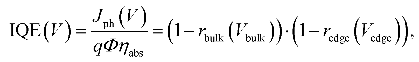
The internal quantum efficiency (IQE) is defined as the ratio of the number of extracted photogenerated charge carrier pairs to the number of absorbed photons. The IQE is less than unity in the presence of recombination. If the charge carriers are localized, the IQE can written as:| |  | (1) |
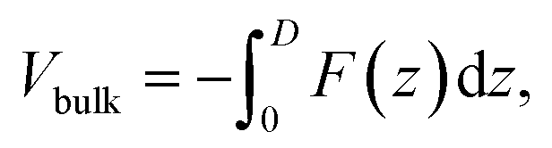
where q is the elementary charge, Φ is the incident photon flux and ηabs is the absorption efficiency. Also, Jph(V) is the photocurrent density at the applied voltage, V, and is equal to the difference between total current density, Jtot, and dark current, Jdark. The recombination efficiencies in the BHJ and at the edges are given by rbulk and redge, with corresponding voltage drops Vbulk and Vedge, respectively. The Vbulk is the macroscopic voltage drop across the BHJ given by:| | 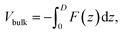 | (2) |
where D is the BHJ thickness, z is the distance to the anode, and F is the average electric field component in the z direction. Due to the random orientation of the donor–acceptor interfaces in a BHJ, the local electric field direction can also be random, leading to nonuniformities in F(z). But F should be monotonic and point from the cathode to the anode for efficient charge extraction to occur. We assume the charge recombination only depends on the local electric field. This assumption can be invalid when the density of photogenerated charges is high, as discussed further in ESI.† The first term, (1 − rbulk (Vbulk)), is the BQE. We write Vedge as:| | | Vedge = Vint + AJtotRedge, | (3) |
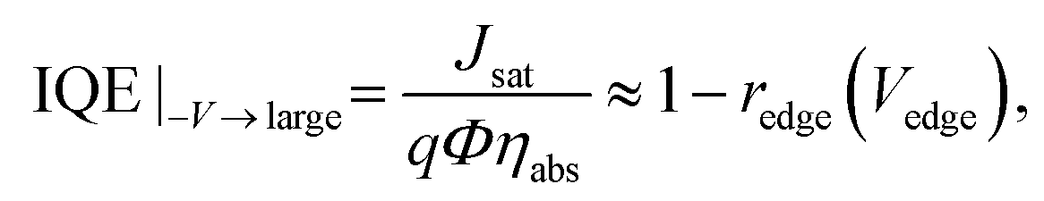
where Vint is the sum of voltages across various interfaces, Redge is the sum of the resistances of all edge layers, and A is the device area. To proceed, two assumptions are made: (i) rbulk ≈ 0 when Vbulk is large; (ii) AJtotRedge ≪ Vint, where the dependence of Vint on applied voltage is much smaller than Vbulk. This latter assumption is based on the understanding that Vint is primarily due to dipoles resulting from the work function difference across the interface. On the other hand, this may not be correct in the presence of a large, mid-energy gap interfacial trap state density.19–22 Assumption (i) results since both geminate and non-geminate recombination vanish at high electric fields.23–25 Assumption (ii) requires the buffer layers to have low resistance compared to the bulk (which is a combination of the junction and internal layer resistances). Therefore, at large reverse bias, eqn (1) becomes:| |  | (4) |
where Jsat is the saturated photocurrent density at large reverse bias. Then, using eqn (1) and (4):| | 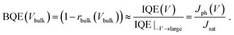 | (5) |
This quantity is the charge collection probability, or normalized photocurrent that has been previously introduced.26,27 In this work we show that BQE is the quantum efficiency specific only to the BHJ, and is independent of the edges in the device. Although BQE is expected to depend on light intensity when high order events (e.g., exciton–exciton annihilation) or charge accumulation are present, we find BQE(Vbulk) is almost independent of intensity at 100 mW cm−2 or lower in the junctions studied (see ESI†).
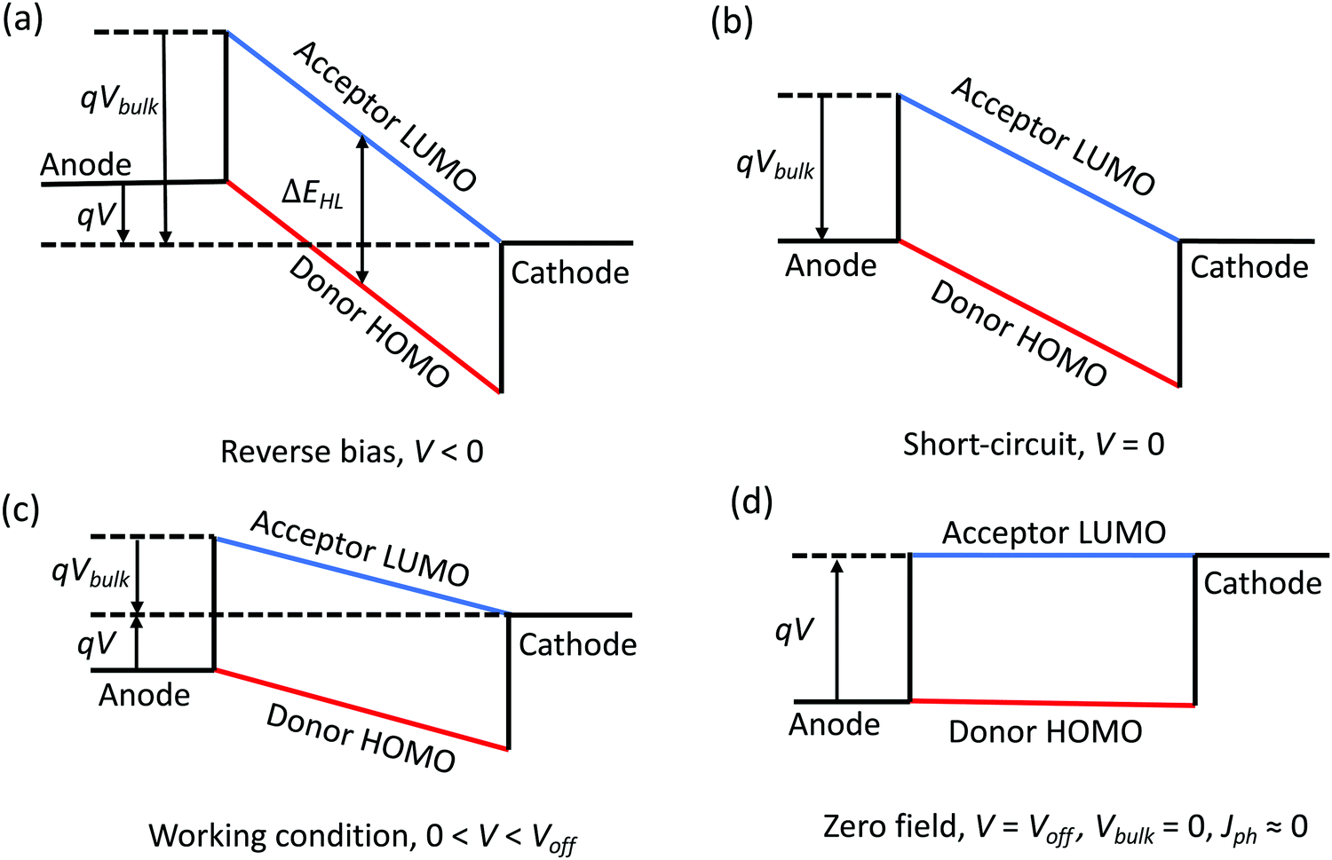
Fig. 1 shows the energy level diagram of an OPV under a forward bias of V < VOC with a schematic indicating the direction of photogenerated current flow. We assume the hole quasi-Fermi level (EFh) is pinned at δ1 above the highest occupied molecular orbital (HOMO) level of the donor on the anode side (ED), and electron quasi-Fermi level (EFe) is pinned at δ2 below the lowest unoccupied molecular orbital (LUMO) level of the acceptor on the cathode side (EA). Then:
| | | qV = EFe − EFh = (EA − δ2) − (ED − δ1) = ΔEHL − qVedge − qVbulk, | (6) |
where Δ
EHL is the energy offset between the acceptor LUMO and the donor HOMO, and
Vedge =
δ1 +
δ2. For convenience, the
Vbulk > 0 is defined as opposite to that of
V, since
Vbulk and
V have opposite signs under OPV operation.
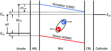 |
| | Fig. 1 Energy level diagram of an OPV under forward bias that is smaller than the open-circuit voltage. The hole quasi-Fermi energy, EFh, is pinned at δ1 above the donor HOMO level on the anode side, while the electron quasi-Fermi energy, EFe, is at δ2 below the acceptor LUMO level on the cathode side. | |
To understand the relationship between the applied voltage, V, and Vbulk, we assume in an ideal OPV that all contacts are ohmic and Vedge = 0. Fig. 2a shows the energy level diagram of the ideal OPV under reverse bias, V < 0. According to eqn (6), Vbulk = ΔEHL/q + |V|. At short-circuit, as shown in Fig. 2b, V = 0 and Vbulk = ΔEHL. Under the solar cell working conditions, V > 0 and Vbulk = ΔEHL/q − V, as shown in Fig. 2c, and Fig. 2d shows the condition when there is no electric field in the BHJ, in which case V = ΔEHL/q, Vbulk = 0.
 |
| | Fig. 2 (a) Energy level diagram of an OPV with ohmic contacts under reverse bias. (b) Energy level diagram of the OPV at short-circuit, (c) under solar cell working conditions, and (d) when there is no electric field across the BHJ. | |
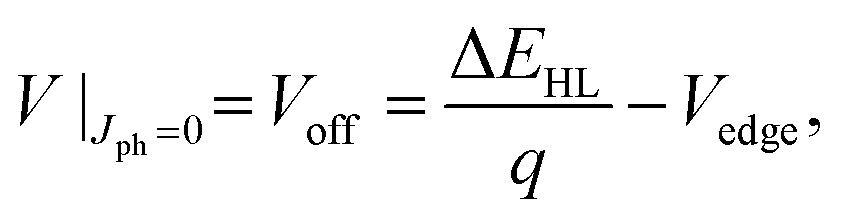
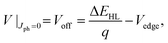
Due to the random orientation of dissociating interfaces and localized charge states in the BHJ, photogenerated charge suffer increased recombination losses compared with planar junctions. Under the condition in Fig. 2d, there is no electric field in the BHJ to help photogenerated charges overcome their Coulomb attraction and guide them towards their respective electrodes. In this case, the probability for the charges to contribute to the photocurrent is low. Here, we approximate Jph = 0 when Vbulk = 0. This assumption is invalid for spatially regular junctions (e.g., a bilayer structure), leading to diffusion dominated photocurrent, or the charges experience band-like transport with no recombination loss (e.g., inorganic semiconductors), or the photogenerated charge density is high and forms a density gradient throughout the BHJ. In this case, eqn (6) becomes:
| |  | (7) |
where we rename
V|
Jph=0 as
Voff, referring to the offset voltage between
V and
Vbulk. Using
eqn (6) and (7), we obtain:
Note that although eqn (4) and (7) are helpful for understanding the physical origins of Jsat and Voff, BQE(Vbulk) can be directly obtained from Jph(V) through eqn (5) and (8). Step-by-step guidance to calculating BQE(Vbulk) is provided in ESI.†
To sum up, our theory rests on three assumptions: (i) rbulk ≈ 0 when Vbulk is large; (ii) the dependence of Vint on applied voltage is much smaller than Vbulk; (iii) when Vbulk = 0, Jph = 0. When these assumptions are valid, then BQE(Vbulk) is a property of the BHJ alone, and consequently is independent of other layers and interfaces within the device. Recombination outside of the BHJ affects Jsat as shown in eqn (4), while voltage drops outside the BHJ affect Voff as in eqn (7).
2.2 BQE degradation equation due to a low concentration of traps
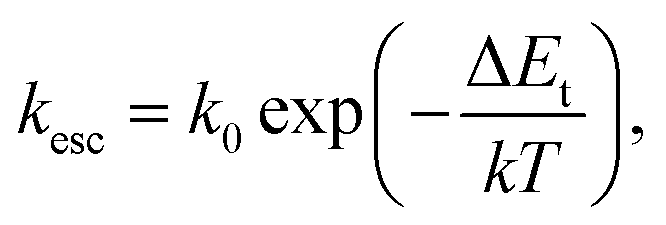
As an OPV ages, its BQE decreases. To understand the aging process, we assume that conductivity within the BHJ is due to thermally-assisted hopping, and that trap sites with energy ΔEt within the energy gap are generated over time. The thermal activated rate for a charge to escape a trap site, kesc, is:28| |  | (9) |
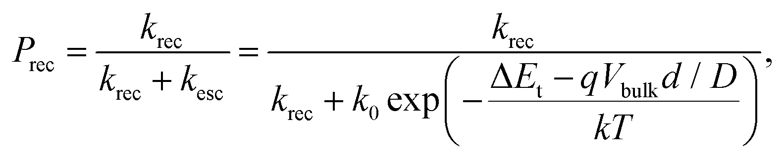
where k0 is a constant, k is the Boltzmann constant and T is the temperature. In an electric field, F, the energy barrier for thermal activation is lowered to ΔEt − qFd, where d is the distance between neighboring sites. Assuming a uniform electric field in a BHJ of thickness D, then F = Vbulk/D. The probability for a trapped charge to recombine is then:| | 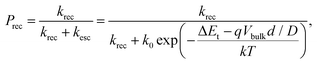 | (10) |
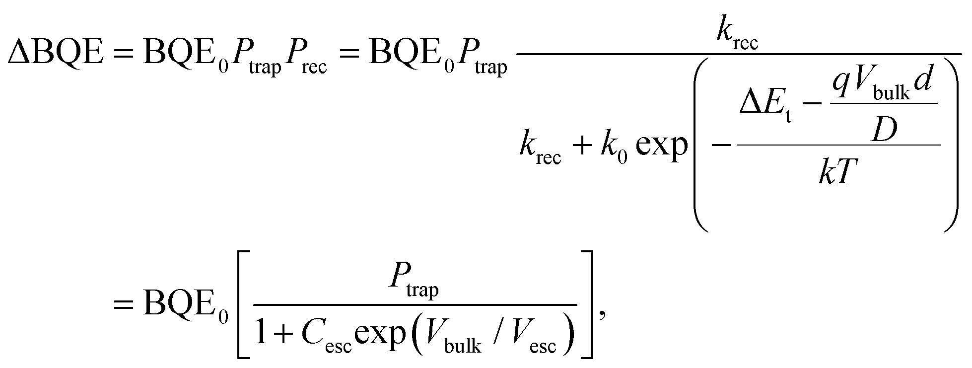
where krec is the recombination rate of trapped charges. In the low trap site density limit where every photogenerated charge gets trapped at most once prior to extraction, the decrease in BQE is:| | 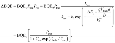 | (11) |
where BQE0 is the BQE of the unaged device, and Ptrap is the probability for photogenerated charges to become trapped during extraction. Also:| |  | (12a) |
and| |  | (12b) |
Here, the escape constant, Cesc, is the ratio of the escape to the recombination rate at zero electric field, and Vesc is the escape voltage. It follows that for efficient charge extraction, Vbulk must be larger than Vesc. Note that eqn (11) is derived in the low trap density limit and does not include other degradation mechanisms such as morphological changes over time.
3. Results
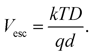
To test that BQE(Vbulk) depends only on photogeneration originating in the BHJ, OPV devices with various BHJs, buffer layers and interface qualities are fabricated. Fig. 3a shows the BQE–Vbulk characteristics of OPVs with identical BHJs comprising DBP as the donor and C70 as the acceptor, but with a variety of anode buffer layers (ABLs). The device structures are: ITO 150 nm/ABL 10 nm/DBP![[thin space (1/6-em)]](https://www.rsc.org/images/entities/char_2009.gif) :C70, 1:8, 54 nm/BPhen 7 nm/Ag 100 nm as shown in the inset. For ease in comparing the BQE–Vbulk data, we define V80 as the Vbulk required to achieve a BQE of 80%, i.e.:
:C70, 1:8, 54 nm/BPhen 7 nm/Ag 100 nm as shown in the inset. For ease in comparing the BQE–Vbulk data, we define V80 as the Vbulk required to achieve a BQE of 80%, i.e.:
 |
| | Fig. 3 (a) BQE–Vbulk characteristics of OPVs with identical bulk heterojunction (BHJ) layers of DBP as the donor and C70 as the acceptor (1:8 by volume, 54 nm thick), and various anode buffer layers (ABLs). Inset: Device structure. (b) Current density–voltage (J–V) characteristics of devices in (a). | |
The charge extraction from a BHJ is more efficient when V80 is small. The V80 along with Voff, Jsat and power conversion efficiencies (PCEs) are provided in Table 1. The BHJ itself has been reported to be highly stable under intense sunlight exposure, albeit with different cathode and anode buffers than used here.29 Full chemical names, chemical structures and frontier orbital energies of materials used in this work can be found in ESI.† The J–V characteristics of each device are shown in Fig. 3b. Although VOC, JSC and FF depend on the choice of ABL, their BQE–Vbulk characteristics are almost identical. With different ABLs, the V80 are similar, while Voff and Jsat vary significantly. The Jsat is chosen to equal Jph at −1 V. The choice of Jsat affects the absolute value of BQE, but not the shape of the BQE–Vbulk characteristics (see ESI†).
Table 1 Device characteristics of OPVs with a DBP:C70 BHJ and various anode buffer layer (ABL) materials
| ABL material |
V
off (V) |
J
sat (mA cm−2) |
V
80 (V) |
PCE (%) |
| WOx |
0.50 ± 0.01 |
12.9 ± 0.3 |
0.43 ± 0.03 |
2.5 ± 0.3 |
| PEDOT:PSS |
0.99 ± 0.01 |
15.0 ± 0.3 |
0.46 ± 0.03 |
7.2 ± 0.3 |
| HAT-CN |
0.63 ± 0.01 |
13.7 ± 0.3 |
0.48 ± 0.03 |
4.1 ± 0.2 |
| MoOx |
0.97 ± 0.01 |
13.8 ± 0.3 |
0.44 ± 0.03 |
5.5 ± 0.2 |
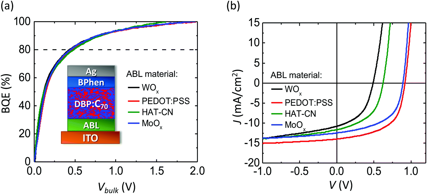
Previously, it has been found that a thin anode interface layer (AIL) inserted between the ABL and BHJ determines the interface voltage, which contributes to Vedge.19Fig. 4a shows the BQE–Vbulk characteristics of OPVs with identical BHJs and a 3 nm-thick AIL of various materials. The device structures are: ITO 150 nm/MoOx 10 nm/AIL 3 nm/DTDCPB:C70, 1:2, 80 nm/BPhen 7 nm/Ag 100 nm as shown in the inset. The J–V characteristics of each device are shown in Fig. 4b, with Voff, Jsat, V80 and PCEs listed in Table 2. The Voff is a sensitive function of the AIL composition, although the BQE–Vbulk characteristics are similar due to the use of the same BHJ in each device.
 |
| | Fig. 4 (a) BQE–Vbulk characteristics of OPVs with identical BHJs comprising DTDCPB as the donor and C70 as the acceptor (1:2 by volume, 80 nm thick) and various anode interface layers (AILs). Inset: Device structure. (b) J–V characteristics of devices in (a). | |
Table 2 Device characteristics of OPVs with a DTDCPB:C70 BHJ and various anode interface layer (AIL) materials
| AIL material |
V
off (V) |
J
sat (mA cm−2) |
V
80 (V) |
PCE (%) |
| BPhen |
0.22 ± 0.01 |
15.4 ± 0.3 |
0.27 ± 0.02 |
0.8 ± 0.1 |
| C60 |
1.02 ± 0.01 |
15.6 ± 0.3 |
0.24 ± 0.02 |
9.4 ± 0.2 |
| C70 |
1.05 ± 0.01 |
14.9 ± 0.3 |
0.23 ± 0.02 |
9.3 ± 0.2 |
| PTCDA |
0.94 ± 0.01 |
14.3 ± 0.3 |
0.22 ± 0.02 |
8.0 ± 0.2 |
| TmPyPB |
0.50 ± 0.01 |
15.3 ± 0.3 |
0.24 ± 0.02 |
3.4 ± 0.2 |
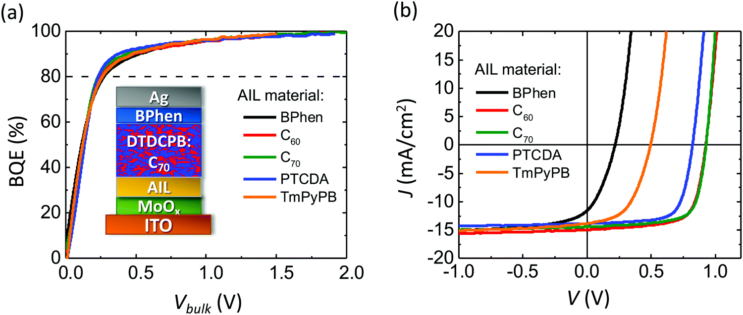
As discussed in Section 2.1, a planar junction can lead to a non-zero Jph even when Vbulk = 0. To evaluate the effectiveness of the use of BQE under such conditions, OPVs with gradient mixing across the BHJs with MoOx or HAT-CN ABLs are fabricated, with their BQE–Vbulk characteristics shown in Fig. 5a. The device structures are: ITO 150 nm/ABL 10 nm//DTDCPB:C70, various gradient mixing ratios, 80 nm/BPhen 7 nm/Ag 100 nm, as shown in the inset. The gradients in C70 concentrations in the legend are from the anode to the cathode side. The J–V characteristics are shown in Fig. 5b, with device parameters provided in Table 3. The BQE–Vbulk characteristics are same for devices with similar gradient mixing ratios, while Jsat, Voff and PCEs vary for different ABLs. The results indicate that the BQE analysis still separates the bulk from edges in such inhomogeneous BHJs.
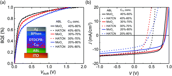 |
| | Fig. 5 (a) BQE–Vbulk characteristics of DTDCPB:C70 OPVs with gradient C70 concentrations from the anode to the cathode side (80 nm), and various anode buffer layers (ABLs). Inset: Device structure. (b) Current density–voltage (J–V) characteristics of devices in (a). | |
Table 3 Device characteristics of OPVs with gradient mixed DTDCPB:C70 BHJs and various anode buffer layers (ABL). The C70 concentrations are referenced from the anode to the cathode side
| ABL material |
C70 conc. (%) |
V
off (V) |
J
sat (mA cm−2) |
V
80 (V) |
PCE (%) |
| MoOx |
40–60 |
0.85 ± 0.01 |
14.7 ± 0.3 |
0.24 ± 0.02 |
7.4 ± 0.1 |
| HAT-CN |
40–60 |
0.61 ± 0.01 |
14.3 ± 0.3 |
0.26 ± 0.02 |
4.0 ± 0.2 |
| MoOx |
30–70 |
0.88 ± 0.01 |
14.1 ± 0.3 |
0.38 ± 0.02 |
7.1 ± 0.2 |
| HAT-CN |
30–70 |
0.36 ± 0.01 |
14.6 ± 0.3 |
0.42 ± 0.02 |
2.0 ± 0.2 |
| MoOx |
20–80 |
0.91 ± 0.01 |
12.9 ± 0.3 |
0.62 ± 0.02 |
5.7 ± 0.2 |
| HAT-CN |
20–80 |
0.43 ± 0.01 |
11.7 ± 0.3 |
0.63 ± 0.02 |
1.7 ± 0.2 |
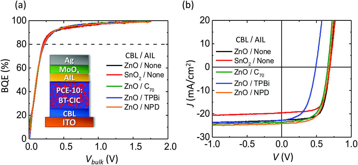
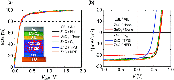
We also determined the BQE of solution-processed, inverted OPVs with PCE-10 as the donor and BT-CIC as the acceptor.30,31Fig. 6a shows BQE–Vbulk characteristics of the OPVs with two different CBLs (ZnO and SnO2) and various AILs. The device structures are: ITO 150 nm/CBL 30 nm/PCE-10:BT-CIC, 1:1.5, 80 nm/AIL 3 nm/MoOx 10 nm/Al 100 nm as shown in the inset. Their J–V characteristics are shown in Fig. 6b, and device parameters are provided in Table 4. Again, all devices have almost identical BQE–Vbulk characteristics. The OPV with a SnO2 CBL has Jsat that is 3 mA cm−2 smaller than that with a ZnO CBL, while various AILs primarily affect Voff.
 |
| | Fig. 6 (a) BQE–Vbulk characteristics of OPVs with identical BHJs of PCE-10 as the donor and BT-CIC as the acceptor (1:1.5 by weight, 80 nm thick) and various cathode buffer layer (CBL)/AIL compositions. Inset: Device structure. (b) J–V characteristics of devices in (a). | |
Table 4 Device characteristics of inverted OPVs with a PCE-10:BT-CIC BHJ and various cathode buffer layer (CBL) and AIL compositions
| CBL/AIL |
V
off (V) |
J
sat (mA cm−2) |
V
80 (V) |
PCE (%) |
| ZnO/none |
0.74 ± 0.01 |
24.1 ± 0.3 |
0.21 ± 0.02 |
10.0 ± 0.2 |
| SnO2/none |
0.77 ± 0.01 |
21.1 ± 0.3 |
0.22 ± 0.02 |
9.1 ± 0.2 |
| ZnO/C70 |
0.72 ± 0.01 |
24.3 ± 0.3 |
0.22 ± 0.02 |
9.7 ± 0.2 |
| ZnO/TPBi |
0.52 ± 0.01 |
24.0 ± 0.3 |
0.21 ± 0.02 |
5.9 ± 0.2 |
| ZnO/NPD |
0.74 ± 0.01 |
25.1 ± 0.3 |
0.21 ± 0.02 |
10.4 ± 0.2 |
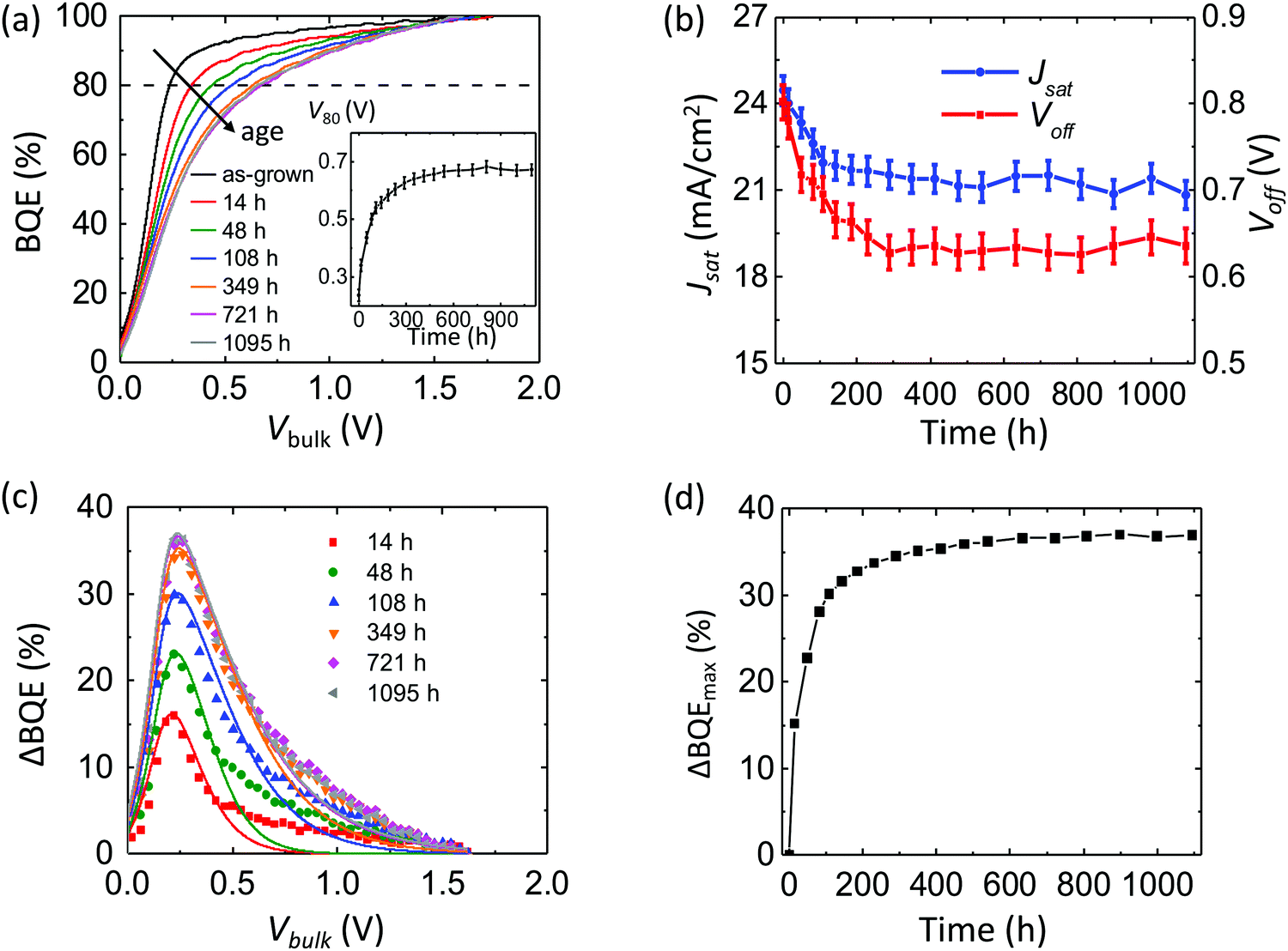
Fig. 7a shows the BQE–Vbulk characteristics of an OPV with DBP:C70 BHJ aged under a white light-emitting diode (LED) array which delivers an equivalent intensity of 27 suns (27 kW m−2, lacking UV content).29 The inset shows V80vs. aging time. The device structure is: ITO 150 nm/MoOx 10 nm/DBP:C70, 1:8, 54 nm/C70 9 nm/TPBi:C70, 1:1, 10 nm/TPBi 3 nm/Ag 100 nm. After 1000 h, V80 increases by approximately 0.2 V. The Voff and Jsatvs. time are shown in Fig. 7b. The Voff remains stable while Jsat decreases by approximately 10%.
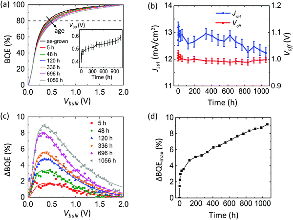 |
| | Fig. 7 (a) BQE–Vbulk characteristics of a DBP:C70 OPV aged under white light with an intensity equivalent to 27 suns. Inset: V80vs. aging time. (b) Voff and Jsatvs. aging time. (c) Experimental (symbols) and fitted (lines) values of the decrease in BQE relative to the as-grown device (ΔBQE) vs. Vbulk at various aging times. (d) Maximum values of ΔBQE vs. aging time. | |
Fig. 7c shows the change in BQE, ΔBQE, relative to the device prior to aging. The experimental (symbols) and results fit to eqn (11) (lines) are in reasonable agreement, assuming Vesc = 0.5 V, which corresponds to a site distance d = 4.1 nm. Values of fitting parameters, Ptrap, Cesc and Vesc, for each line are provided in ESI.†Fig. 7d shows the maximum value of ΔBQE vs. aging time. Since ΔBQE ∝ Ptrap, the results suggest that the trap site density increases linearly with time after an initial burn-in.
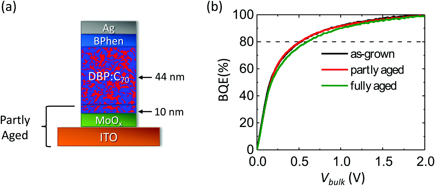
To separate the contributions of the MoOx layer and the MoOx/BHJ interface from the BHJ in the BQE decrease in Fig. 7a, the lower section of the OPV including the ITO layer, the MoOx layer and 10 nm of the DBP:C70 BHJ were aged for 17 days under the same conditions as in Fig. 7a before the remaining layers are deposited (called the partly aged device), as shown in Fig. 8a. For comparison, a complete device with the same structure was fabricated (the as-grown device) and aged for the same amount of time at 27 suns (the fully aged device). The BQE–Vbulk characteristics of the partly aged device are compared with those of the as-grown device and the fully aged device, as shown in Fig. 8b. The device parameters of the unaged and aged devices are provided in Table 5. Although the MoOx layer and the MoOx/BHJ interface experience intense light exposure, the partly aged device has almost identical BQE–Vbulk characteristics as the as-grown device. The Voff and Jsat of the partly aged device, however, drop significantly.
 |
| | Fig. 8 (a) Structure of the partly aged and fully aged OPVs. The ITO layer, MoOx layer and bottom 10 nm of the BHJ were aged under white light with an intensity equivalent to 27 suns for 17 days in the partly aged device. (b) BQE–Vbulk characteristics of the partly aged device, the as-grown device, and the fully aged device. | |
Table 5 Device characteristics of DBP:C70 OPVs with various aging procedures
| Device |
V
off (V) |
J
sat (mA cm−2) |
V
80 (V) |
PCE (%) |
| As-grown |
0.94 ± 0.01 |
13.3 ± 0.3 |
0.52 ± 0.03 |
5.3 ± 0.2 |
| Partly Aged |
0.82 ± 0.01 |
12.7 ± 0.3 |
0.52 ± 0.03 |
4.5 ± 0.2 |
| Fully Aged |
0.94 ± 0.01 |
12.8 ± 0.3 |
0.60 ± 0.03 |
5.1 ± 0.2 |
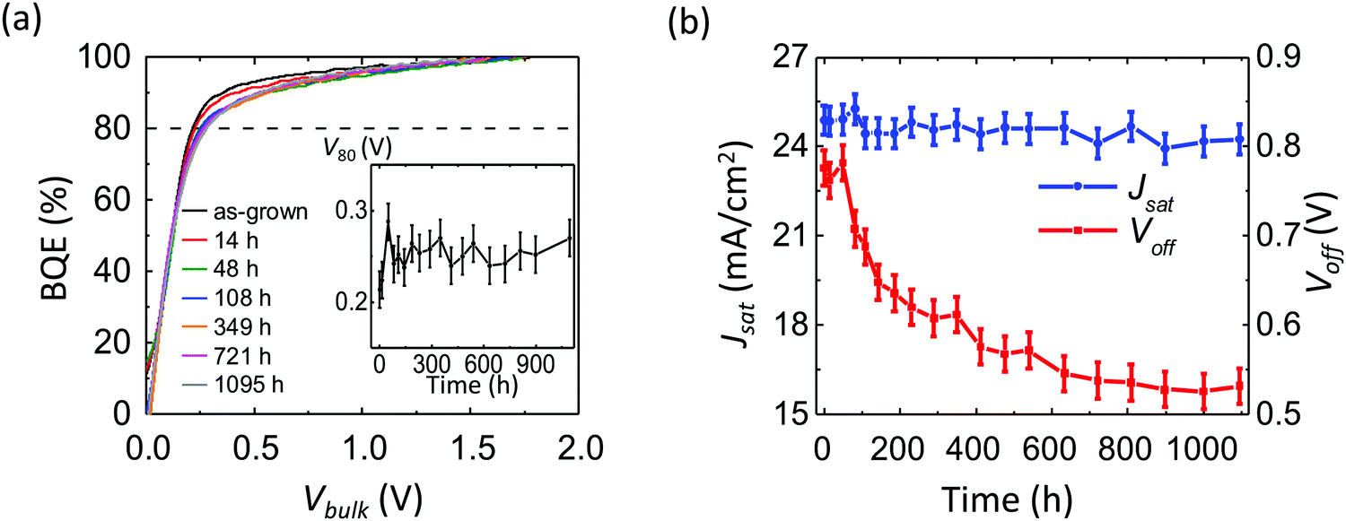
Fig. 9a shows the BQE–Vbulk characteristics of an OPV aged under 1 sun intensity, simulated AM 1.5G illumination from a Xe-arc lamp. The device structure is: ITO 150 nm/ZnO 30 nm/PCE-10:BT-CIC, 1:1.5, 80 nm/MoOx 10 nm/Al 100 nm. The V80 experiences a significant increase of 0.4 V after 300 h, see inset. Fig. 9b shows the Voff and Jsatvs. time. The Voff drops by 0.15 V during aging, while the Jsat drops by 3.5 mA cm−2. Fig. 9c shows the experimental (symbols) and fitted (lines) ΔBQE vs. Vbulk. The average Vesc is 0.2 V, corresponding to a site distance d = 10 nm. The fitted lines depart from the experimental data at large Vbulk, suggesting that the low trap site density assumption used to derive eqn (11) is invalid. The maximum values of ΔBQE vs. aging time are shown in Fig. 9d, where it is observed that the decrease in BQE saturates after 300 h.
 |
| | Fig. 9 (a) BQE–Vbulk characteristics of an inverted OPV with a PCE-10:BT-CIC BHJ and a ZnO CBL aged under simulated AM 1.5G illumination. Inset: V80vs. aging time. (b) Voff and Jsatvs. aging time. (c) Experimental (symbols) and fitted (lines) decrease in BQE (ΔBQE) vs. Vbulkvs. aging time. (d) The maximum values of ΔBQE vs. aging time. | |
Fig. 10a shows the BQE–Vbulk characteristics of an OPV with a C60-SAM inserted at the ZnO/BHJ interface, and the inset shows the V80vs. aging time. The BQE–Vbulk characteristics are stable after an initial burn-in. The Voff and Jsatvs. aging time is shown in Fig. 10b. The Jsat is stable, while Voff drops by 0.24 V.
 |
| | Fig. 10 (a) BQE–Vbulk characteristics of a PCE-10:BT-CIC OPV with a self-assembled monolayer (C60-SAM) inserted between the BHJ and the ZnO layer under simulated AM 1.5G illumination. Inset: V80vs. aging time. (b) Voff and Jsatvs. aging time. | |
4. Discussion
Conventional metrics used to analyze OPV performance such as VOC, JSC and FF often have entangled correlations with the device structure, making it difficult to evaluate the effectiveness of a particular layer in the photogeneration process. On the other hand, BQE, Jsat and Voff, can separate the BHJ properties from the edges. As shown in Fig. 3a, 4a, 5a and 6a, devices with different ABL, CBL or AIL layers have similar BQE–Vbulk characteristics. Indeed, the BQE–Vbulk characteristics are unaffected even for layers that severely reduce PCE (e.g., WOx ABLs and BPhen AILs) and BHJs with varying mixing ratios across the active region. The impacts of the contacts, buffer layers and interfaces are incorporated in Voff and Jsat, which depend on voltage drops and recombination at the edges, respectively. For clarification, the separation of the bulk properties from the edges is based on experimental observation, which is elucidated by the theory in Section 2.1. In cases when an energy barrier exists at one of the interfaces leading to a “S-shaped” J–V characteristics,32 the BQE analysis is no longer able to separate the bulk properties from the edges (see ESI†). This failure is likely due to charge accumulation at the contact, causing Vint to have a large dependence on V.
Several mechanisms can lead to the degradation of OPV performance: morphological changes33–35 or chemical changes (e.g., photo-bleaching and molecule fragmentation)29,36,37 in the BHJ, degradation of the electrodes,38,39 degradation of the buffer layers,40–43 chemical reactions and diffusion between BHJ and edge layers, etc.44–47 As shown in Fig. 7a and b, the BQE of the DBP:C70 OPV decreases under illumination, whose trend can be fit with eqn (11), as shown in Fig. 7c. The Voff remains almost constant, suggesting that there is no significant increase in the voltage across the interface during aging. The Jsat experiences a decrease of 1 mA cm−2, which may be due to increased trapping within the buffer layers.
In the partly aged device in Fig. 8a, only the lower section was exposed to illumination. This device has nearly identical BQE–Vbulk characteristics as the as-grown device, while the BQE of the fully aged device is reduced, as shown in Fig. 8b. This suggests that the MoOx and the MoOx/BHJ interface are not responsible for the decrease in BQE observed in Fig. 7a. The Jsat of the partly aged device is similar to that of the fully aged device, which is 0.5 mA cm−2 smaller than that of the as-grown device, as shown in Table 4, indicating that aging of the lower edge layers (nearest the substrate) account for the decrease in Jsat observed in Fig. 7b. The partly aged device has a Voff that is 0.12 V smaller compared with that of the as-grown and fully aged devices. This is possibly due to an energy barrier between the aged and unaged parts of the BHJ.
For solution-processed PCE-10:BT-CIC BHJs, the BQE decreases relative to the fresh device with a 0.4 V increase in V80 after 1000 h of aging under 1 sun intensity, simulated AM 1.5G illumination, as shown in Fig. 9a. The Voff drops by 0.15 V while Jsat decreases by 3.5 mA cm−2 (see Fig. 9b). The fitted lines depart from the experimental data at large Vbulk in Fig. 9c, suggesting the existence of trapped charges even at large Vbulk. This is possibly because a high trap site density results in multiple trapping events for each charge during charge extraction, increasing the recombination probability beyond that predicted by eqn (11) at large Vbulk (see Ptrap in Table S3, ESI†). The ΔBQE saturates after 300 h, as shown in Fig. 9d.
To study whether the decrease in BQE is caused by changes in morphology or material decomposition in the BHJ,34–37 or changes external to the active region such as photocatalytic reactions at the ZnO interface,44,45 a C60-SAM was inserted at the ZnO/BHJ interface to prevent interactions with the BHJ. With the C60-SAM, the BQE decrease is eliminated except for a small burn-in effect, as shown in Fig. 10a. The OPV loss of efficiency with aging is, therefore, most likely due to chemical reactions between the BHJ and ZnO layer, while the BHJ itself appears to be stable. In addition, we heated the device in darkness at 45 °C and found that the BQE is not affected, while the Voff decreases (see ESI†).
5. Conclusions
In this work, we introduced a method to analyze OPV performance by directly measuring the charge photogeneration efficiency within the BHJ using the bulk quantum efficiency that is extracted directly from the OPV J–V characteristics. The BQE analysis was used to separate the properties of the BHJ from the device peripheral regions (interfaces, buffer layers, contacts) for both vacuum- and solution-processed OPVs. Compared with conventional metrics such as VOC, JSC and FF, the BQE, Voff and Jsat, introduced in this work are determined by either the active or the edge regions, providing physical insights into the photogeneration process. This method is derived for systems with localized charge carriers and isotropic dissociating interfaces, and thus might have broader applications such as for perovskite solar cells.
The BQE analysis is applied to quantitatively study degradation mechanisms in both vacuum and solution deposited devices. In solution-processed NFA OPVs, we show that the primary mechanism of performance degradation is induced by the ZnO buffer layer. By inserting a self-assembled monolayer at the BHJ/ZnO interface, the degradation is significantly suppressed and the BHJ is stabilized.
6. Experimental section
6.1 Device fabrication
All OPVs were fabricated on ITO coated glass substrates (Lumtec Corp.) with a sheet resistance of 15 Ω sq−1. The ITO anodes were patterned into 2 mm wide strips. The substrates were cleaned using a detergent (tergitol solution) and solvents (acetone and isopropanol) and exposed to ultraviolet ozone for 10 min prior to thin film deposition.
For vacuum-processed OPVs, the substrates were transferred into a vacuum thermal evaporation (VTE) chamber with a base pressure of 10−7 torr, and all layers were deposited at rates between 0.2 to 1.6 Å s−1. The deposition rates and thicknesses were measured using quartz crystal monitors and calibrated post-growth using variable-angle spectroscopic ellipsometry. Metal cathodes were deposited through 2 mm wide shadow mask openings oriented orthogonal to the ITO strips, forming device areas of 4 mm2.
The ZnO CBL employed in solution-processed OPVs was spun onto the substrates at 4000 rpm for 1 min using a sol–gel ZnO precursor solution (Sigma-Aldrich Inc.), and then thermally annealed at 160 °C for 30 min in air. The SnO2 CBL was deposited from a nanocrystal dispersion (Sigma-Aldrich Inc.). The SnO2 dispersion was diluted to 0.4 wt% by adding isopropanol and spun onto the substrates at 4000 rpm for 1 min. The sample was then thermally annealed in air for 30 min at 160 °C. The C60-SAM (1-Material Inc.) was dissolved at 1.5 mg mL−1 in chlorobenzene(CB):tetrahydrofuran(THF) (2:1 vol%) solution and stirred at 300 rpm overnight. The solution was then spin-coated at 3500 rpm for 1 min, and thermally annealed at 110 °C for 10 min. A second spin-coating using CB:THF (2:1 vol%) solution spun at the same speed was applied on top of the film to remove residual C60-SAM molecules that are not chemically bonded to the surface. The PCE10:BT-CIC blend was dissolved at a total concentration of 16 mg mL−1 in 9:1 CB:chloroform solution with a 1:1.5 weight ratio, and stirred at 300 rpm overnight at 65 °C. The solution was subsequently spun onto the sample at 4000 rpm for 1 min. The AIL, MoOx and Al cathode were deposited via the same procedures as the vacuum-processed OPVs.
For the devices in Fig. 7b, the MoOx and the lower 10 nm of the BHJ were deposited on two identical ITO coated glass substrates in the VTE chamber and encapsulated in N2 atmosphere. One sample (later fabricated into the partly aged device) was exposed to 27 suns for 17 days while the other (later fabricated into the as-grown device) was kept in darkness. Then both sample packages were opened and the remaining device layers including 44 nm thick BHJ, BPhen and Ag cathodes were deposited in the VTE chamber using the same procedures as the vacuum-processed OPVs. After the J–V measurement, the as-grown device was aged at 27 suns for 17 days which is referred to as the fully aged device.
6.2 Device aging and J–V measurement
The simulated solar illumination was produced using a large-area Xe-arc lamp filtered to approximate an AM 1.5G reference, and the intensity was calibrated to 1 sun intensity (1 kW m−2) using a calibrated Si photodiode (National Renewable Energy Laboratory). The 27 suns white light source was achieved using high-intensity white LED arrays. The intensity was calibrated using the as-grown PCE-10:BT-CIC OPV in Fig. 8a. The OPV is illuminated using a solar simulator, and the Jsc is recorded as Jsc,AM1.5G. The OPV is then illuminated by the LED array with the intensity concentrated with a silver-coated reflective tube and a 10% transmissive neutral-density filter. The power of the LED array was adjusted so that the OPV produces a Jsc equivalent to 2.7Jsc at AM 1.5G. The details of the aging setup and the spectra of the light sources are found elsewhere.29
The J–V characteristics were measured inside a N2 glovebox at room temperature using a semiconductor parameter analyzer (Agilent 4156C) with a 1 kW m−2 simulated AM 1.5G illumination source. Fluctuations in contact resistance during the J–V measurement results in randomness in the Jph near Vbulk = 0. In this case, the Voff is determined by aligning the rising edges of the BQE–Vbulk curves (see ESI†).
Conflicts of interest
One of the authors (SRF) has an equity interest in a sponsor of this work (Universal Display Corp.). The conflict is under management by the University of Michigan Office of Research.
Acknowledgements
We thank Dr Shaocong Hou, Dr Dejiu Fan and Xinjing Huang for helpful discussions. This work was partially supported by the Department of the Navy, Office of Naval Research under Award No. N00014-17-1-2211 (K. D., experiment and analysis, X. H., experiment, Y. L., experiment, S. R. F., analysis) and Universal Display Corporation.
References
- R. R. Lunt, N. C. Giebink, A. A. Belak, J. B. Benziger and S. R. Forrest, J. Appl. Phys., 2009, 105, 053711 CrossRef.
- G. Chen, H. Sasabe, Z. Wang, X.-F. Wang, Z. Hong, Y. Yang and J. Kido, Adv. Mater., 2012, 24, 2768 CrossRef CAS.
- R. Pandey, Y. Zou and R. J. Holmes, Appl. Phys. Lett., 2012, 101, 033308 CrossRef.
- Y. Sun, G. C. Welch, W. L. Leong, C. J. Takacs, G. C. Bazan and A. J. Heeger, Nat. Mater., 2012, 11, 44 CrossRef CAS.
- T. S. van der Poll, J. A. Love, T.-Q. Nguyen and G. C. Bazan, Adv. Mater., 2012, 24, 3646 CrossRef CAS.
- J. J. M. Halls, C. A. Walsh, N. C. Greenham, E. A. Marseglia, R. H. Friend, S. C. Moratti and A. B. Holmes, Nature, 1995, 376, 498 CrossRef CAS.
- G. Yu, J. Gao, J. C. Hummelen, F. Wudl and A. J. Heeger, Science, 1995, 270, 1789 CrossRef CAS.
- H. Bässler, Phys. Status Solidi B, 1993, 175, 15 CrossRef.
- X. Liu, K. Ding, A. Panda and S. R. Forrest, ACS Nano, 2016, 10, 7619 CrossRef CAS.
- K. Ding, X. Liu and S. R. Forrest, Nano Lett., 2018, 18, 3180 CrossRef CAS.
- Y. L. Lin, M. A. Fusella and B. P. Rand, Adv. Energy Mater., 2018, 8, 1702816 CrossRef.
- A. A. Bakulin, A. Rao, V. G. Pavelyev, P. H. M. van Loosdrecht, M. S. Pshenichnikov, D. Niedzialek, J. Cornil, D. Beljonne and R. H. Friend, Science, 2012, 335, 1340 CrossRef CAS.
- M.-H. Jao, H.-C. Liao and W.-F. Su, J. Mater. Chem. A, 2016, 4, 5784 RSC.
- B. Qi and J. Wang, Phys. Chem. Chem. Phys., 2013, 15, 8972 RSC.
- R. A. J. Janssen and J. Nelson, Adv. Mater., 2013, 25, 1847 CrossRef CAS.
- N. K. Elumalai and A. Uddin, Energy Environ. Sci., 2016, 9, 391 RSC.
- K. Vandewal, K. Tvingstedt, A. Gadisa, O. Inganäs and J. V. Manca, Phys. Rev. B: Condens. Matter Mater. Phys., 2010, 81, 125204 CrossRef.
- L. J. A. Koster, V. D. Mihailetchi, H. Xie and P. W. M. Blom, Appl. Phys. Lett., 2005, 87, 203502 CrossRef.
- K. Ding and S. R. Forrest, Phys. Rev. Appl., 2020, 13, 054046 CrossRef CAS.
- M. T. Greiner, M. G. Helander, W.-M. Tang, Z.-B. Wang, J. Qiu and Z.-H. Lu, Nat. Mater., 2011, 11, 76 CrossRef.
- N. B. Kotadiya, H. Lu, A. Mondal, Y. Ie, D. Andrienko, P. W. M. Blom and G.-J. A. H. Wetzelaer, Nat. Mater., 2018, 17, 329 CrossRef CAS.
- K. Sotthewes, R. van Bremen, E. Dollekamp, T. Boulogne, K. Nowakowski, D. Kas, H. J. W. Zandvliet and P. Bampoulis, J. Phys. Chem. C, 2019, 123, 5411 CrossRef CAS.
- D. Credgington, F. C. Jamieson, B. Walker, T.-Q. Nguyen and J. R. Durrant, Adv. Mater., 2012, 24, 2135 CrossRef CAS.
- T. Kirchartz, B. E. Pieters, J. Kirkpatrick, U. Rau and J. Nelson, Phys. Rev. B: Condens. Matter Mater. Phys., 2011, 83, 115209 CrossRef.
- T. M. Clarke, A. Ballantyne, S. Shoaee, Y. W. Soon, W. Duffy, M. Heeney, I. McCulloch, J. Nelson and J. R. Durrant, Adv. Mater., 2010, 22, 5287 CrossRef CAS.
- A. K. K. Kyaw, D. H. Wang, V. Gupta, W. L. Leong, L. Ke, G. C. Bazan and A. J. Heeger, ACS Nano, 2013, 7, 4569 CrossRef CAS.
- S. R. Cowan, R. A. Street, S. Cho and A. J. Heeger, Phys. Rev. B: Condens. Matter Mater. Phys., 2011, 83, 035205 CrossRef.
- A. Miller and E. Abrahams, Phys. Rev., 1960, 120, 745 CrossRef CAS.
- Q. Burlingame, X. Huang, X. Liu, C. Jeong, C. Coburn and S. R. Forrest, Nature, 2019, 573, 394 CrossRef CAS.
- X. Che, Y. Li, Y. Qu and S. R. Forrest, Nat. Energy, 2018, 3, 422 CrossRef CAS.
- Y. Li, J.-D. Lin, X. Che, Y. Qu, F. Liu, L.-S. Liao and S. R. Forrest, J. Am. Chem. Soc., 2017, 139, 17114 CrossRef CAS.
- A. Sundqvist, O. J. Sandberg, M. Nyman, J.-H. Smått and R. Österbacka, Adv. Energy Mater., 2016, 6, 1502265 CrossRef.
- M. Jørgensen, K. Norrman and F. C. Krebs, Sol. Energy Mater. Sol. Cells, 2008, 92, 686 CrossRef.
- B. Ray and M. A. Alam, Appl. Phys. Lett., 2011, 99, 033303 CrossRef.
- W. R. Mateker and M. D. McGehee, Adv. Mater., 2017, 29, 1603940 CrossRef.
- M. O. Reese, A. M. Nardes, B. L. Rupert, R. E. Larsen, D. C. Olson, M. T. Lloyd, S. E. Shaheen, D. S. Ginley, G. Rumbles and N. Kopidakis, Adv. Funct. Mater., 2010, 20, 3476 CrossRef CAS.
- W. R. Mateker, T. Heumueller, R. Cheacharoen, I. T. Sachs-Quintana, M. D. McGehee, J. Warnan, P. M. Beaujuge, X. Liu and G. C. Bazan, Chem. Mater., 2015, 27, 6345 CrossRef CAS.
- S. Cros, M. Firon, S. Lenfant, P. Trouslard and L. Beck, Nucl. Instrum. Methods Phys. Res., Sect. B, 2006, 251, 257 CrossRef CAS.
- F. So and D. Kondakov, Adv. Mater., 2010, 22, 3762 CrossRef CAS.
- E. Bovill, N. Scarratt, J. Griffin, H. Yi, A. Iraqi, A. R. Buckley, J. W. Kingsley and D. G. Lidzey, Appl. Phys. Lett., 2015, 106, 073301 CrossRef.
- R. Rösch, D. M. Tanenbaum, M. Jørgensen, M. Seeland, M. Bärenklau, M. Hermenau, E. Voroshazi, M. T. Lloyd, Y. Galagan, B. Zimmermann, U. Würfel, M. Hösel, H. F. Dam, S. A. Gevorgyan, S. Kudret, W. Maes, L. Lutsen, D. Vanderzande, R. Andriessen, G. Teran-Escobar, M. Lira-Cantu, A. Rivaton, G. Y. Uzunoğlu, D. Germack, B. Andreasen, M. V. Madsen, K. Norrman, H. Hoppe and F. C. Krebs, Energy Environ. Sci., 2012, 5, 6521 RSC.
- A. Manor, E. A. Katz, T. Tromholt and F. C. Krebs, Adv. Energy Mater., 2011, 1, 836 CrossRef CAS.
- S. Trost, T. Becker, A. Polywka, P. Görrn, M. F. Oszajca, N. A. Luechinger, D. Rogalla, M. Weidner, P. Reckers, T. Mayer and T. Riedl, Adv. Energy Mater., 2016, 6, 1600347 CrossRef.
- S. Park and H. J. Son, J. Mater. Chem. A, 2019, 7, 25830 RSC.
- Y. Jiang, L. Sun, F. Jiang, C. Xie, L. Hu, X. Dong, F. Qin, T. Liu, L. Hu, X. Jiang and Y. Zhou, Mater. Horiz., 2019, 6, 1438 RSC.
- J. Li, Q. Dong, N. Li and L. Wang, Adv. Energy Mater., 2017, 7, 1602922 CrossRef.
- B. P. Rand, P. Peumans and S. R. Forrest, J. Appl. Phys., 2004, 96, 7519 CrossRef CAS.
Footnote |
| † Electronic supplementary information (ESI) available. See DOI: 10.1039/d0ee03885g |
|
| This journal is © The Royal Society of Chemistry 2021 |
Click here to see how this site uses Cookies. View our privacy policy here. 
 *abc
*abc