
 Open Access Article
 This Open Access Article is licensed under a Creative Commons Attribution-Non Commercial 3.0 Unported Licence
Hybrid MoS2/PEDOT:PSS transporting layers for interface engineering of nanoplatelet-based light-emitting diodes†
Roberto
Sorrentino
*a,
Robyn
Worsely
b,
Paola
Lagonegro
a,
Christian
Martella
 c,
Adriana
Alieva
b,
Guido
Scavia
a,
Francesco
Galeotti
a,
Mariacecilia
Pasini
a,
Benoit
Dubertret
d,
Sergio
Brovelli
e,
Alessandro
Molle
*c,
Cinzia
Casiraghi
*b and
Umberto
Giovanella
*a
c,
Adriana
Alieva
b,
Guido
Scavia
a,
Francesco
Galeotti
a,
Mariacecilia
Pasini
a,
Benoit
Dubertret
d,
Sergio
Brovelli
e,
Alessandro
Molle
*c,
Cinzia
Casiraghi
*b and
Umberto
Giovanella
*a
aCNR, Istituto di Scienze e Tecnologie Chimiche “Giulio Natta” (SCITEC), via A. Corti 12, 20133, Milano, Italy. E-mail: roberto.sorrentino@scitec.cnr.it; umberto.giovanella@scitec.cnr.it
bThe University of Manchester, Department of Chemistry, Oxford Rd, Manchester M13 9PL, UK. E-mail: cinzia.casiraghi@manchester.ac.uk
cCNR-IMM, Unit of Agrate Brianza, via C. Olivetti 2, 20864 Agrate Brianza (MB), Italy. E-mail: alessandro.molle@mdm.imm.cnr.it
dLaboratoire de Physique et d'Etude des Matériaux, ESPCI-ParisTech, PSL Research University, Sorbonne Université UPMC, Université Paris 06, CNRS, 10 rue Vauquelin, 75005 Paris, France
eDipartimento di Scienza dei Materiali, Università degli Studi di Milano-Bicocca, via Cozzi 55, 20125 Milano, Italy
First published on 1st June 2021
Abstract
Colloidal semiconductor nanoplatelets (NPLs) are a subgroup of quantum confined materials that have recently emerged as promising active materials for solution processed light-emitting diodes (LEDs) thanks to their peculiar structural and electronic properties as well as their reduced dimensionality. Nowadays, the conventional structure for NPL-based LEDs makes use of poly(3,4-ethylenedioxythiophene) polystyrene sulfonate (PEDOT:PSS) as a hole transporting layer (HTL). This is a well-known conjugated conductive polymer because it leads to high LED efficiency, though it has limited stability in air due to its intrinsic acidity and hygroscopicity. Here, we develop a nanocomposite aqueous ink, obtained by blending commercial PEDOT:PSS with water-based, stable and highly concentrated molybdenum disulfide (MoS2) nanosheets, obtained via liquid phase exfoliation (LPE), which is suitable as a HTL for solution processed NPL-based LEDs. We demonstrate that the MoS2 additive effectively works as a performance booster in unpackaged devices, thereby prolonging the lifetime up to 1000 hours under ambient conditions. Moreover, the addition of MoS2 induces a modification of the anode interface properties, including a change in the work function and a significant enhancement of the permittivity of the HTL.
Introduction
Colloidal quantum confined materials are solution-processable semiconductor nanocrystals1,2 that allow emission wavelength tunability by size modification and narrow emission linewidths.3–5 In particular, a new promising class of solution-processable materials, CdSe/CdZnS NPLs, has been used in LEDs due to their easy control on the synthesis procedure and their high color purity. So far, more attention has been devoted to pursuing record efficiencies with these materials rather than towards stable devices, frequently encapsulating them to avoid air exposure, rendering the production process more expensive.6,7Beyond the intrinsic performance of the emitter, other interfacial layers at the anode (hole transporting layers/electron blocking layers, HTLs) and at the cathode (electron injecting layers/hole blocking layers, EILs) interfaces need to be incorporated in the device architecture. These interlayers are an effective tool to optimize the charge injection selectivity and to reduce non-radiative recombination and contact resistance,8–11 thus favoring charge carrier balancing and exciton confinement into the emitting layer. PEDOT:PSS is the most used conducting polymer as a HTL because it is commercially available, it features a work function (WF ∼ −5.2 eV) that well matches with that of the transparent anode (i.e. indium doped tin oxide – ITO), it is easily processable from aqueous solution by spin coating deposition techniques, and it allows for achieving record efficiencies in LEDs6 and optoelectronic devices in general.12 However, the hygroscopic and acidic (pH ∼ 1.5) nature of PEDOT:PSS13 leads to a rapid degradation of the device anode.14 In particular, its acidity and the absorption of water molecules promote the etching of indium from the ITO/PEDOT:PSS interface, then causing indium diffusion and ultimately leading to fast deterioration of the device.15
Recently, other alternative HTLs have been explored in optoelectronic devices14 such as neutral-pH conducting conjugated polymers,16 metal oxides,17,18 carbon-based materials19 and two-dimensional (2D) transition metal dichalcogenides (TMDs).20–22 The latter class of materials (with a general formula of MX2, where M is a transition metal and X is a chalcogenide) combines energy levels that are suitable for optoelectronics with high carrier mobilities and excellent optical transparency.23–25 Moreover, owing to the mass-scale feasibility of the liquid phase exfoliation method,26 it is possible to obtain a large quantity of nanosheets and easily process them using simple approaches, such as printing techniques.27,28,29,30,31 In both organic- and perovskite-based solar cells, the use of TMDs led to higher power conversion efficiency.32–34 Following these exciting results, TMDs have been recently exploited as HTLs in LEDs,35,36 showing a significantly improved charge-injection capacity in the devices and hence, an improved energy conversion efficiency for photon emission. Despite the good efficiency achieved, the use of TMDs is limited by some disadvantages. For instance, TMD deposition is hardly controllable and it usually ends up with pinholes or inhomogeneities that create shunts in the devices. Moreover, TMDs usually need post-treatment at relatively high temperatures (i.e. 300 °C) and/or exposure to ultraviolet light/ozone to adjust their WF.34,37,38
An alternative strategy consists of mixing PEDOT:PSS with TMDs. This approach has been successfully applied to solar cells, leading to higher performance,39–42 and to other kinds of devices.43 Nonetheless, only a few works have implemented this scheme on LEDs, but the low concentration of exfoliated MoS2 used (∼0.5 mg mL−1) did not allow for a fair comparison with the reference device and/or UV–ozone treatment was still needed.20,44,45
In this work, we investigate the use of a nanocomposite aqueous ink, based on a mixture of PEDOT:PSS and highly concentrated MoS2 nanosheets, as a HTL in NPL-LEDs. The aim of our study is to understand whether the addition of MoS2 to PEDOT:PSS can improve the drawbacks of this interface layer and have a positive impact on the performance of the corresponding device. Our results show that the presence of MoS2 can influence PEDOT:PSS properties such as acidity, hygroscopicity, work function, conductivity and permittivity. The appropriate formulation of the ink proves the beneficial impacts mostly on long-term higher efficiency for not-encapsulated devices exposed to environmental conditions, with respect to the reference LEDs prepared with PEDOT:PSS alone.
Results and discussion
Water-based MoS2 dispersions were efficiently produced by LPE using organic dyes as dispersant agents, as reported earlier29,46 and briefly described in the Experimental section. This formulation, in particular, was selected because it allows us to achieve highly concentrated (∼1 mg mL−1) and stable dispersions in water, which therefore can be directly mixed with PEDOT:PSS. The details of the materials characterization in this respect are reported elsewhere.45,47 The nanosheets have an average lateral size (<n>) of ∼66 nm and a thickness (<t>) of ∼5 nm (Fig. S1†). The Raman spectrum of a spin-coated film (Fig. S2†) shows the two characteristic peaks of the MoS2 layer, namely, the in-plane, E12g, and out-of-plane, A1g, modes. The frequency positions of the modes are E12g ∼ 379.4 cm−1 and A1g ∼ 404.6 cm−1, thus revealing a frequency separation of 25.2 cm−1.48 It should be noted, however, that this peak separation cannot be used to quantify the number of layers in solution-processed MoS2. The MoS2 dispersion was mixed with the PEDOT:PSS solution through a short sonication process (10 minutes) in order to produce the nanocomposite inks investigated. The MoS2/PEDOT:PSS solid ratios of the final solutions were 3.3%, 6.6%, and 10%. The composite material was deposited onto glass slides by optimizing the spin coating conditions (see Table S1†). The films obtained had a thickness of ∼30 nm and transparency >90% at 450 nm. Hence, the addition of the MoS2 ink to PEDOT:PSS does not strongly affect the transparency, up to the amount used in this work (Fig. S3†).Atomic force microscopy (AFM) was performed on thin films deposited on an ITO substrate to investigate the presence and distribution of MoS2 nanosheets in the overall film. Topography images confirmed the average size of the nanosheets and showed a homogeneous distribution of the MoS2 flakes (Fig. 1a). The root mean square (RMS) surface roughness of the thin films increases from 1.4 nm to 6.2 nm with increasing content of MoS2 in PEDOT:PSS.
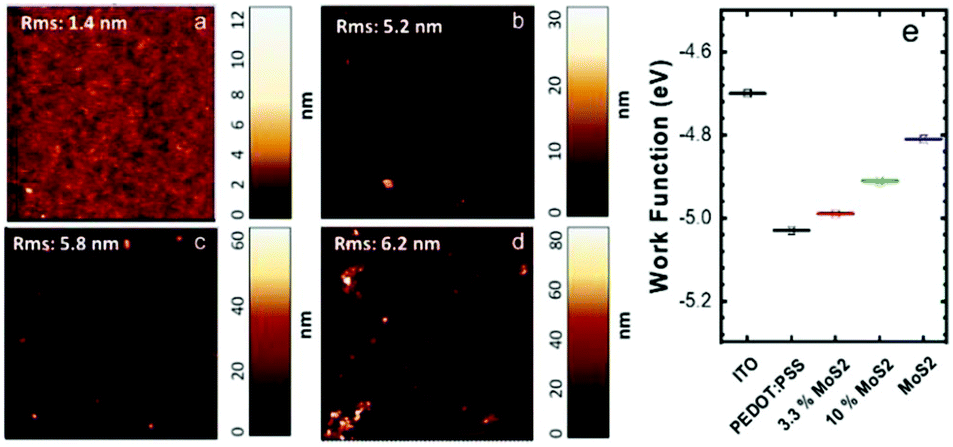 | ||
| Fig. 1 (a) AFM 10 μm × 10 μm height images of thin films of PEDOT:PSS (a), 3.3% MoS2 (b), 6.6% MoS2 (c) and 10% MoS2 (d); the root mean square roughness (RMS) is reported for each composition. (e) KPFM measurements for PEDOT:PSS, MoS2 and nanocomposite materials with different ratios of MoS2/PEDOT:PSS spin coated on ITO and bare ITO substrates; values were collected as a reference. Error bar ± 10 meV. | ||
The WFs of ITO, PEDOT:PSS, liquid phase exfoliated MoS2 and nanocomposite films were measured by Kelvin probe force microscopy (KPFM). The values measured for PEDOT:PSS and MoS2 sheet films were similar to those reported in the literature.49,50 Compared to the pristine PEDOT:PSS, the MoS2 WF is slightly lower and the inclusion of MoS2 nanosheets in PEDOT:PSS can reduce the |WF| by ∼0.1–0.3 eV, depending on the MoS2 content (Fig. 1b), thus resulting in an increase of the energy barrier for hole injection.20
CdSe/CdZnS core–shell NPLs were selected as an emitter for their unique properties such as easy processability and efficient emission with high colour purity.51,52 Fig. S4† shows their optical properties and a transmission electron microscopy (TEM) image, showing the typical size and shape of the NPLs. NPL-based LEDs were fabricated using a direct architecture ITO/HTL/HIL/NPLs/EIL/Al (HIL: hole injecting/electron blocking layer). A reference device incorporating only PEDOT:PSS as a HTL was fabricated to investigate the impact of MoS2 addition on PEDOT:PSS. All the layers were deposited from solution by following the strategy of orthogonal solvents, paying attention not to dissolve or damage the previously deposited layer. Both PEDOT:PSS and the nanocomposite material were processed from an aqueous solution, obtaining a HTL with a thickness of 30 nm. Poly[(9,9-dioctylfluorenyl-2,7-diyl)-co-(4,4′-(N-(4-sec-butylphenyl)diphenylamine)] (TFB, scheme in Fig. 2a) is a commercial polymer acting as a HIL, preferred to polyvinylcarbazole (PVK) as previously used52 due to its superior stability and good hole mobility (μh > 10−4 cm2 V−1 s−1). TFB was deposited from chlorobenzene to give a 35 nm thick film. The red-emitting layer (40 nm) of NPLs was spin-coated from a hexane solution to preserve the interface with TFB. The lab- made poly[(2,7-(9,9′-bis(6′-diethoxylphosphorylhexyl)-fluorene)-alt-(2,7-(9,9′-bis(6′′-trimethyl-ammonium bromide)hexyl)-fluorene)]53 (P1, scheme in Fig. 2b) was deposited as a EIL (25 nm) from alcohol solution, in which NPLs are not soluble due to their oleic acid ligands.
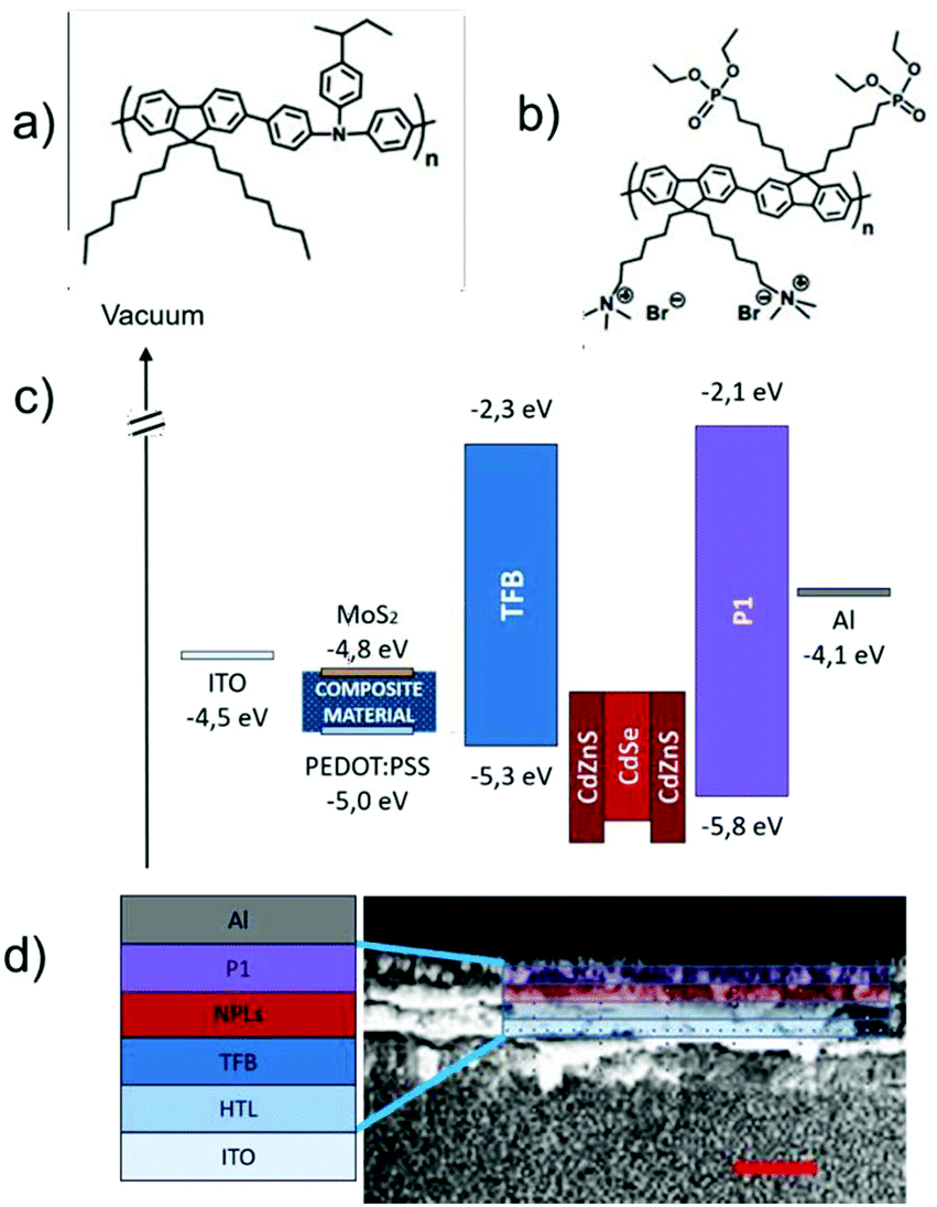 | ||
| Fig. 2 (a) TFB and (b) P1 structure schemes. (c) Flat-band energy diagram of the devices. (d) Sketch of a sandwiched direct structure LED and a cross section image of NPL-based LEDs (scale bar 150 nm). | ||
The time-resolved PL measurements of the NPLs, TFB and ionic polymer films indicate that the emission efficiency of the NPLs (PL quantum yield of 40 ± 5%) is unaffected by the presence of the organic transport layers.45,52 Finally, 100 nm of a thermally evaporated bare aluminium cathode was used to complete the devices.
The behaviour of the PEDOT:PSS-only reference device (hereafter named device “D0”) was compared with the nanocomposite PEDOT:PSS + MoS2 with different MoS2 concentrations (3.3% in device D1, 6.6% in D2 and 10% in D3, Table 1). Note that devices with neat MoS2 as a HTL did not exhibit a diode behaviour (not shown in the manuscript), possibly due to the extremely low conductivity of a network of small MoS2 flakes. The devices D0–3 switched on in the range of 3–3.2 V and did not show changes either in electroluminescence (EL) or in CIE parameters upon increasing the MoS2 content. The EL spectra showed a sharp profile with a peak centred at 658 nm and a FWHM of ∼28 nm (Fig. 3a and S5†), showing deep red EL, almost saturated with CIE values of x = 0.69; y = 0.28 (Fig. 3b).
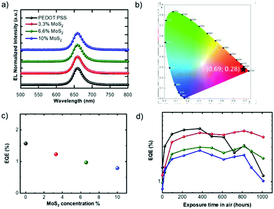 | ||
| Fig. 3 Comparison between PEDOT:PSS and nanocomposite PEDOT:PSS + MoS2 device performances. (a) EL normalized spectra, vertically shifted for clarity; (b) CIE 1931 chromaticity diagram; (c) starting EQE vs. MoS2 content; and (d) EQE% vs. exposure time under ambient conditions. The same color scheme is used. | ||
External quantum efficiencies (EQEs), defined as the ratio between the number of emitted photons and the number of electrons injected into the device, measured under a nitrogen atmosphere (hereafter called “starting EQEs”) are shown in Fig. 3c. D1 exhibited higher maximum luminance (up to 2000 cd m−2) with respect to the control device (1300 cd m−2, Fig. S6†), though a slightly lower starting EQE of D1 compared to the D0 device was recorded, similarly to previous observations.45 The optimal thickness of the HTL was kept constant in all the devices and the reason for the different EQEs should most probably be the increase of the energy barrier for hole injection upon addition of MoS2, as evidenced by KPFM. The possible aggregation of MoS2 nanosheets in the blend with PEDOT:PSS in D2 and mostly in D3 devices, with a rougher interface, explains the further EQE decrease in D2 and D3.
Based on our earlier findings,45 due to the acid and hygroscopic nature of PEDOT:PSS, the addition of MoS2 flakes to the HTL is expected to have a strong impact on the stability of the devices once they are transferred in air without encapsulation. Therefore, we set up a test in which the devices were stored in air at a temperature (T) of ∼ 25 °C and the humidity (H) in the range of ∼40–60% without any kind of encapsulation or protection from oxygen and/or moisture for over 1000 hours (∼40 days) and periodically measured. All the devices were manufactured in a single set, so they experienced the same changes under the lab atmosphere.
Up to 400 hours of exposure, the behaviours of the D0–3 devices were pretty much mutually similar and showed an approximately 3.5 times increase in the EQE values (Fig. 3d). This was due to the fact that in CdSe/CdZnS NPLs, it is easier to inject electrons from the Al cathode rather than holes from PVK; using TFB instead of PVK, the injection of holes into the valence band of NPLs was improved while the insertion of P1 reduced the electron flow into the emitter's conduction band. Still, the charge carrier balance had probably not yet been achieved. The first hours of air exposure positively impacted the EQE of all devices because of a partial oxidation of the P1/Al interface that modifies the electron injection properties.52,54
If the devices are exposed for a longer time in air, the presence of MoS2 in the HTL becomes critical for EQE behaviour (Fig. 3c, empty squares). In fact, in the range of 400–800 hours, the D0 device lost about 50% of its maximum efficiency, while a constant EQE was recorded for D1–3. The test was continued up to 1000 hours, thus showing in all devices a progressive decrease in the EQEs, which however remained higher than the corresponding initial values in the case of D1–3.
The observed prolonged stability is the result of a favourable combination of different effects produced by the addition of MoS2. First of all, a reduced acidity of the HTL solution (pH from 1.5 to 5) is achieved with the addition of a neutral solution of 3.3% of MoS2 while the hygroscopicity of the HTL is only slightly affected as evidenced by contact angle measurements (29° ± 1 and 27° ± 2 for PEDOT:PSS and 3.3% hybrid, respectively). The dilution of PEDOT:PSS could reduce the doping level, explaining the reduction in the conductivity upon increasing the pH.14 Notably, by increasing the MoS2 content, a higher resistance is measured, as shown in Fig. S7† which is likely due to the use of small MoS2 nanosheets, which have poor conductivity. The mobility of the MoS2 monolayer (200 cm2 V−1 s−1)55 is definitely higher than that of the pristine PEDOT:PSS one (0.045 cm2 V−1 s−1)56 but in a network of small MoS2 flakes, the net mobility can be much reduced owing to a percolation threshold that limits the charge conduction.57 Additionally, the presence of trap states in MoS2 may allow the charges to accumulate and eventually facilitate charge separation, thus promoting dipole formation.
To further assess how the MoS2 additive nanosheets affect the physical properties of PEDOT:PSS, we carried out a comparative impedance spectroscopy study. The devices were fabricated with the same geometry as for LEDs, but with the architecture ITO/PEDOT:PSS/Al and ITO/PEDOT:PSS + MoS2 (3.3%)/Al. The HTL with 3.3% MoS2 was chosen for its more relevant LED behaviour over time. In Fig. 4a and b the Bode plots of the absolute impedance |Z| and the phase angle φ as a function of the small-signal frequency are shown, while Fig. 4c shows the Nyquist plot, displaying the real and imaginary parts of the impedance Z. The device behaviour in both cases is consistent with a simplified Randles model circuit applied to the general case of an electrochemical cell.58,59 As such, the LEDs can be modelled by a contact (ohmic) resistance that is in series with a parallel capacitance between a layer capacitance and a charge transfer resistance. The latter two quantities are related to the integral layer permittivity and the energy loss processes under applied small signal solicitation (e.g. dipoles), respectively.
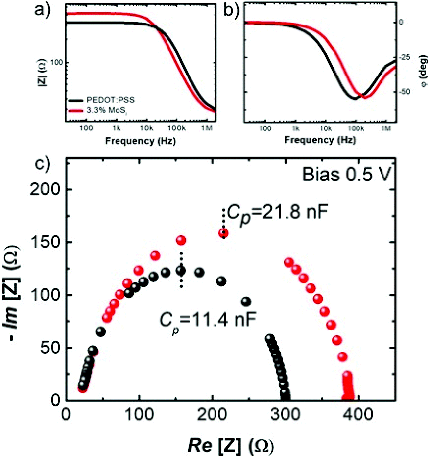 | ||
| Fig. 4 Comparison between ITO/PEDOT:PSS/Al and ITO/PEDOT:PSS + MoS2 (3.3%)/Al through impedance spectroscopy characterization. Bode plots of the (a) absolute impedance and (b) phase angle as a function of the small-signal frequency. (c) Nyquist plot displaying the real and imaginary parts of the impedance. | ||
Two facts can be stressed out. (1) The low-frequency impedance module in the Bode plot reveals a higher charge transfer resistance in the MoS2-added LED that can be generally due to an energy loss from a higher density of charge trapping centres.
(2) The double layer capacitance extracted from the Nyquist plot (under a bias of 0.5 V) increases from 11.4 nF up to 21.8 nF when the MoS2 nanosheets are added, thereby reflecting a significant MoS2-induced enhancement of the permittivity from 6.3 up to 12.8, which is in good agreement with the literature.60
The enhanced capacitance is attributed to the presence of trap states of the interrupted percolative paths of MoS2 that allow charge accumulation, providing a higher permittivity, which in turn facilitates the formation of stronger dipoles at the interfaces. As a consequence, the charges can be more efficiently injected in the active layer of the device,61,62 thereby counterbalancing the reduced hole injection due to the shift in the WF observed by KP analysis.
Experimental
Synthesis of MoS2
Water-based MoS2 dispersions were prepared by stabilizer-assisted liquid phase exfoliation in water. Namely, bulk MoS2 powder (Sigma Aldrich; molybdenum(IV) sulphide powder; <2 μm; purity 99%) was added to deionized water (18.2 MΩ cm) at a concentration of 3 mg mL−1, along with 1-pyrenesulphonic acid sodium salt, used as a stabilizer (Sigma Aldrich, purity >97.0%), at a concentration of 1 mg mL−1. This mixture was subsequently sonicated at a constant temperature of 20 °C for 120 h using a 300 W Hilsonic HS 1900/Hilsonic FMG 600 bath sonicator. An initial 20 minute centrifugation step, performed at 3500 rpm using a Sigma 1–14 K refrigerated centrifuge, was then implemented to enable any remaining un-exfoliated bulk powder to be discarded from the sonicated solution. Finally, the resultant dispersion was passed through a series of washing steps, in order to remove any excess stabilizer, and replace the solvent with fresh de-ionized water. The pH of the MoS2 dispersion was neutral as exfoliation was performed under neutral conditions and the excess surfactant was removed.63 The concentration of the final dispersion was ∼1 mg mL−1, as determined using the UV-visible spectroscopy (Varian Cary 5000 UV−vis spectrometer) and the Beer–Lambert law, using an extinction coefficient at 672 nm of 3400 L g−1 m−1.PEDOT:PSS + MoS2 nanocomposite
The concentrations used are calculated by considering the solid fraction ratio of MoS2 (1 mg mL−1) and PEDOT:PSS (15 mg mL−1). Different quantities were mixed resulting in 0%, 3.3%, 6.6% and 10% of MoS2 with respect to the PEDOT:PSS solid fraction. After mixing the two materials, the solutions were sonicated for 10 minutes in a bath sonicator to create a homogeneous blend of the two materials and deposited by spin coating, at different speeds, to maintain constant thicknesses.Device fabrication and characterization
For LED fabrication, glass substrates (25 mm × 25 mm × 1.1 mm) coated with indium tin oxide (ITO) with a sheet resistance of 15 Ω per sq were used. The substrates were mechanically cleaned with acetone and optical paper, sonicated for 20 minutes at 50 °C in acetone and then 20 minutes in 2-propanol and treated with 3 mbar plasma for 10 minutes. Immediately after the plasma treatment, a 30 nm thick PEDOT:PSS (Clevios Al 4083) film was spin coated in air over ITO. The film was thermally annealed at 120 °C inside a N2 filled glovebox for 10 minutes. After decreasing the temperature of the substrate, a layer of the poly[(9,9-dioctylfluorenyl-2,7-diyl)-co-(4,4′-(N-(4-sec-butylphenyl)diphenylamine)] (TFB) hole-transport layer was spin coated from an 8 mg mL−1 chlorobenzene solution and annealed at 150 °C for 10 minutes. NPLs (received from Nexdot) were sonicated for 20 minutes before being spin-coated from a 30 mg mL−1 hexane solution to obtain an active layer of 40 nm. The deposition of the polymer ETL was performed by spin coating of the P1 polymer, dissolved in pure methanol (5 mg mL−1) to obtain a thickness of 25 nm. The metal cathode consisting of a 90 nm aluminium layer was finally thermally evaporated under high vacuum (8 × 10⁻⁷ bar). The final device area was 6.1 mm2. All the thicknesses were characterized using a Bruker profilometer.A Keithley 2602 source meter was used to measure the current–voltage–luminance characteristics of the devices. The light output was measured using a calibrated silicon photodetector.
The EL spectra were recorded using a Spex 270 M spectrometer. AFM height imaging and contact potential difference (CPD) measurements were performed with a commercial NT-MDT NTEGRA AFM using noncontact (NSG10) or Pt coated (NSG/Pt) tips.
Conclusions
In conclusion, we incorporated water-based, stable and highly concentrated MoS2 nanosheets in the well-known and largely employed PEDOT:PSS as hole transporting layers in nanocrystal light-emitting diodes. After the optimization of the ink composition and the study of the film morphology, we investigated the performances of LEDs, with CdSe/CdZnS colloidal semiconductor nanoplatelets as an emitter, by integrating the hybrid HTLs.Kelvin probe measurements of the polymer nanocomposite films showed a fine tunability of the work functions with respect to pure PEDOT:PSS. An enhanced permittivity value was revealed by impedance spectroscopy on the hybrid HTL. Furthermore, a reduction of the acidity of the HTL by the addition of MoS2 was achieved, but accompanied by a lower conductivity of the ink film.
Our work shows that the combination of these factors has a strong impact on the device performance, mainly when exposed to air. The use of the MoS2/PEDOT:PSS composite as a HTL, with a proper formulation, allows achieving, after initial air annealing, stable EQEs with respect to the reference device during the aging test of unpackaged LEDs up to 1000 hours under air exposure.
These results demonstrate that a TMD-based nanocomposite material can efficiently improve the performance of NPL-based LEDs without the need for its encapsulation. This strategy may hold outstanding potential for solution processed photonic devices in the field of artificial lighting and portable displays, and the same scheme can be readily transposed to other devices, such as QD-LEDs and OLEDs, making the encapsulation less critical.
Author contributions
Roberto Sorrentino (R. S.) optimized the nanocomposite material concentration, and fabricated and tested the devices. R. S. analyzed the data under the supervision of Umberto Giovanella (U. G.). Paola Lagonegro (P. L.) performed the investigation (film morphology by means of AFM). Guido Scavia (G. S.) performed the investigation (Kelvin probe measurements). Christian Martella (C. M.) performed the investigation (Raman and impedance spectroscopy) under the supervision of Alessandro Molle (A. M.). Francesco Galeotti (F. G.) and Mariacecilia Pasini (M. P.) synthesized the polymer used as an electron injecting layer. Benoit Dubertret (B. D.) synthesized the NPLs used as an active material. Sergio Brovelli (S. B.) performed spectroscopic studies on NPLs and polymers. Robyn Worsely (R. W.) exfoliated and characterized the MoS2 sheets and Adriana Alieva (A. A.) obtained the SEM cross section image of the devices under the supervision of Cinzia Casiraghi (C. C.). R. S., A. M. and U. G. conceived the idea for the project, designed the experiments and wrote the first draft. All authors contributed to the writing of the manuscript.Conflicts of interest
There are no conflicts to declare.Acknowledgements
U. G. acknowledges the MIUR-PRIN project Prot. 20172M3K5N. R. S and U. G. acknowledge Dr Silvia Luzzati (CNR-SCITEC) for the helpful discussion. C. C. and A. M. acknowledge the financial support from the Royal Society (IES\R3\170384); furthermore, C. C. thanks the European Research Council (ERC) under the European Union's Horizon 2020 research and innovation programme under grant agreement no. 770047. R. W. acknowledges Hewlett-Packard Company for the financial support in the framework of the CDT graphene. A. M. acknowledges Dr S. Spiga and S. Cocco (CNR-IMM) for useful discussion and technical assistance.Notes and references
- C. B. Murray, C. R. Kagan and M. G. Bawendi, Annu. Rev. Mater. Sci., 2000, 30, 545–610 Search PubMed.
- X. G. Peng, Nano Res., 2009, 2, 425–447 Search PubMed.
- E. Jang, S. Jun, H. Jang, J. Lim, B. Kim and Y. Kim, Adv. Mater., 2010, 22(28), 3076–3080 Search PubMed.
- O. Chen, J. Zhao, V. P. Chauhan, J. Cui, C. Wong, D. K. Harris, H. Wei, H.-S. Han, D. Fukumura, R. K. Jain and M. G. Bawendi, Nat. Mater., 2013, 12, 445–451 Search PubMed.
- J. Zhou, M. Zhu, R. Meng, H. Qin and X. Peng, J. Am. Chem. Soc., 2017, 139(46), 16556–16567 Search PubMed.
- Y. Kelestemur, Y. Shynkarensko, M. Anni, S. Yakunin, M. L. De Giorgi and M. V. Kovalenko, ACS Nano, 2019, 13, 13899–13909 Search PubMed.
- B. Liu, Y. Altintas, L. Wang, S. Shendre, M. Sharma, H. Sun, E. Mutlugun and H. V. Demir, Adv. Mater., 2019, 1905824 Search PubMed.
- H. H. Liao, L. M. Chen, Z. Xu, G. Li and Y. Yang, Appl. Phys. Lett., 2008, 92, 173303 Search PubMed.
- C. He, C. Zhong, H. Wu, R. Yang, W. Yang, F. Huang, G. C. Bazan and Y. Cao, J. Mater. Chem., 2010, 20, 2617–2622 Search PubMed.
- M. J. Hartel, J. Subbiah and F. So, J. Disp. Technol., 2013, 9, 6 Search PubMed.
- A. Castelli, F. Meinardi, M. Pasini, F. Galeotti, V. Pinchetti, M. Lorenzon, L. Manna, I. Moreels, U. Giovanella and S. Brovelli, Nano Lett., 2015, 15(8), 5455–5464 Search PubMed.
- W. Han, G. Ren, J. Liu, Z. Li, H. Bao, C. Liu and W. Guo, ACS Appl. Mater. Interfaces, 2020, 12(44), 49297–49322 Search PubMed.
- A. Garcia, G. C. Welch, E. L. Ratcliff, D. S. Ginley, G. C. Bazan and D. C. Olson, Adv. Mater., 2012, 24(39), 5368–5373 Search PubMed.
- J. Cameron and P. J. Skabara, Mater. Horiz., 2020, 7, 1759 Search PubMed.
- M. P. de Jong, L. J. van IJzendoorn and M. J. A. de Voigt, Appl. Phys. Lett., 2000, 77, 2255 Search PubMed.
- S. Ahn, S.–H. Jeong, T.–H. Han and T.–W. Lee, Adv. Opt. Mater., 2017, 5, 1600512 Search PubMed.
- J. J. Jasieniak, J. Seifter, J. Jo, T. Mates and A. J. Heeger, Adv. Funct. Mater., 2012, 22, 2594–2605 Search PubMed.
- S. I. Lee, G. J. Yun, J. W. Kim, G. Hanta, K. Liang, L. Kojvic, L. S. Hui, A. Turak and W. Y. Kim, Sci. Rep., 2019, 9, 2411 Search PubMed.
- L. B. R. Lee, J.-W. Kim, D. Kang, D. W. Lee, S.-J. Ko, H. J. Lee, C.-L. Lee, J. Y. Kim, H. S. Shin and M. H. Song, ACS Nano, 2012, 6(4), 2984–2991 Search PubMed.
- C. Kim, T. P. Nguyen, Q. Van Le, J.-M. Jeon, H. W. Jang and S. Y. Kim, Adv. Funct. Mater., 2015, 25, 4512–4519 Search PubMed.
- X. Gu, W. Cui, H. Li, Z. Wu, Z. Zeng, S.–T. Lee, H. Zhang and B. Sun, Adv. Energy Mater., 2013, 3, 1262–1268 Search PubMed.
- G. J. Choi, Q. Van Le, K. S. Choi, K. C. Kwon, H. W. Jang, J. S. Gwag and S. Y. Kim, Adv. Mater., 2017, 29, 1702598 Search PubMed.
- M. Chhowalla, H. S. Shin, G. Eda, L.-J. Li, K. P. Loh and H. Zhang, Nat. Chem., 2013, 5, 263–275 Search PubMed.
- X. Li and H. Zhu, J. Materiomics, 2015, 1(1), 33–44 Search PubMed.
- N. Huo and G. Konstantatos, Adv. Mater., 2018, 30, 1801164 Search PubMed.
- Y. Hernandez, V. Nicolosi, M. Lotya, F. M. Blighe, Z. Sun, S. De, I. T. McGovern, B. Holland, M. Byrne, Y. K. Gun'Ko, J. J. Boland, P. Niraj, G. Duesberg, S. Krishnamurthy, R. Goodhue, J. Hutchison, V. Scardaci, A. C. Ferrari and J. N. Coleman, Nat. Nanotechnol., 2008, 3, 563–568 Search PubMed.
- T. Carey, S. Cacovich, G. Divitini, J. Ren, A. Mansouri, J. M. Kim, C. Wang, C. Ducati, R. Sordan and F. Torrisi, Nat. Commun., 2017, 8, 1–11 Search PubMed.
- A. G. Kelly, T. Hallam, C. Backes, A. Harvey, A. S. Esmaeily, I. Godwin, J. Coelho, V. Nicolosi, J. Lauth, A. Kulkarni, S. Kinge, L. D. A. Siebbeles, G. S. Duesberg and J. N. Coleman, Science, 2017, 356, 69–73 Search PubMed.
- D. McManus, S. Vranic, F. Withers, V. Sanchez-Romaguera, M. Macucci, H. Yang, R. Sorrentino, K. Parvez, S.-K. Son, G. Iannaccone, K. Kostarelos, G. Fiori and C. Casiraghi, Nat. Nanotechnol., 2017, 12, 343–350 Search PubMed.
- L. Ng, G. Hu, R. Howe, X. Zhu, Z. Yang, C. G. Jones and T. Hasan, Printing of Graphene and Related 2D Materials, Springer, 2018 Search PubMed.
- G. Hu, J. Kang, L. W. T. Ng, X. Zhu, R. C. T. Howe, C. G. Jones, M. C. Hersam and T. Hasan, Chem. Soc. Rev., 2018, 47, 3265–3300 Search PubMed.
- Y. Lin, B. Adilbekova, Y. Firdaus, E. Yengel, H. Faber, M. Sajjad, X. Zheng, E. Yarali, A. Seitkhan, O. M. Bakr, A. El-Labban, U. Schwingenschlögl, V. Tung, I. McCulloch, F. Laquai and T. D. Anthopoulos, Adv. Mater., 2019, 31, 1902965 Search PubMed.
- B. Adilbekova, Y. Lin, E. Yengel, H. Faber, G. Harrison, Y. Firdaus, A. El-Labban, D. H. Anjum, V. Tung and T. D. Anthopoulos, J. Mater. Chem. C, 2020, 8, 5259–5264 Search PubMed.
- G. Tang, P. You, Q. Tai, A. Yang, J. Cao, F. Zheng, Z. Zhou, J. Zhao, P. K. L. Chan and F. Yan, Adv. Mater., 2019, 31(24), 1807689 Search PubMed.
- K. Guo, C. Si, C. Han, S. Pan, G. Chen, Y. Zheng, W. Zhu, J. Zhang, C. Sund and B. Wei, Nanoscale, 2017, 9, 14602 Search PubMed.
- J. Sun, Y. Choi, Y. J. Choi, S. Kim, J.-H. Park, S. Lee and J. H. Cho, Adv. Mater., 2019, 1803831 Search PubMed.
- K. C. Kwon, C. Kim, Q. V. Le, S. Gim, J. M. Jeon, J. Y. Ham, J. L. Lee, H. W. Jang and S. Y. Kim, ACS Nano, 2015, 9, 4146 Search PubMed.
- X. Yang, W. Fu, W. Liu, J. Hong, Y. Cai, C. Jin, M. Xu, H. Wang, D. Yang and H. Chen, J. Mater. Chem. A, 2014, 2, 7727 Search PubMed.
- W. Xing, Y. Chen, X. Wu, X. Xu, P. Ye, T. Zhu, Q. Guo, L. Yang, W. Li and H. Huang, Adv. Funct. Materials, 2017, 27(32), 1701622 Search PubMed.
- D. Wang, N. K. Elumalai, MdA. Mahmud, H. Yi, M. B. Upama, R. A. Lee Chin, G. Conibeer, C. Xu, F. Haque, L. Duan and A. Uddin, Synth. Met., 2018, 246, 195–203 Search PubMed.
- M. S. Ramasamy, K. Y. Ryu, J. W. Lim, A. Bibi, H. Kwon, J. E. Lee, D. H. Kim and K. Kim, Nanomaterials, 2019, 9(9), 1328 Search PubMed.
- Y. Choi, S. Jung, N. K. Oh, J. Lee, J. Seo, U. Kim, D. Koo and H. Park, ChemNanoMat, 2019, 5(8), 1050–1058 Search PubMed.
- Y. Yang, H. Deng and Q. Fu, Mater. Chem. Front., 2020, 4, 3130–3152 Search PubMed.
- X. Zhang, W. Li, Z. Ling, Y. Zhang, J. Xu, H. Wang, G. Chena and B. Wei, J. Mater. Chem. C, 2019, 7, 926–936 Search PubMed.
- P. Lagonegro, C. Martella, B. M. Squeo, F. Carulli, G. Scavia, A. Lamperti, F. Galeotti, B. Dubertret, M. Pasini, S. Brovelli, A. Molle and U. Giovanella, ACS Appl. Electron. Mater., 2020, 2(5)), 1186–1192 Search PubMed.
- H. Yang, F. Withers, E. Gebremedhn, E. Lewis, L. Britnell, A. Felten, V. Palermo, S. Haigh, D. Beljonne and C. Casiraghi, 2D Mater., 2014, 1, 11012 Search PubMed.
- D. McManus, A. Dal Santo, P. B. Selvasundaram, R. Krupke, A. LiBassi and C. Casiraghi, Flexible Printed Electron., 2018, 3(3), 034005 Search PubMed.
- C. Lee, H. Yan, L. E. Brus, T. F. Heinz, J. Hone and S. Ryu, ACS Nano, 2010, 4(5), 2695–2700 Search PubMed.
- http://www.heraeus.com/media/media/hec/documents_hec/data_sheets_hep/Clevios_P_VP_AI_4083 .
- T. P. Nguyen, W. Sohn, J. H. Oh, H. W. Jang and S. Y. Kim, J. Phys. Chem. C, 2016, 120(18), 10078–10085 Search PubMed.
- B. Mahler, B. Nadal, C. Bouet, G. Patriarche and B. Dubertret, J. Am. Chem. Soc., 2012, 134(45), 18591–18598 Search PubMed.
- U. Giovanella, M. Pasini, M. Lorenzon, F. Galeotti, C. Lucchi, F. Meinardi, S. Luzzati, B. Dubertret and S. Brovelli, Nano Lett., 2018, 18, 3441–3448 Search PubMed.
- F. Carulli, G. Scavia, E. Lassi, M. Pasini, F. Galeotti, S. Brovelli, U. Giovanella and S. Luzzati, J. Colloid Interface Sci., 2019, 538, 611–619 Search PubMed.
- T. Cheng, Z. Wang, S. Jin, F. Wang, Y. Bai, H. Feng, B. You, Y. Li, T. Hayat and Z. Tan, Adv. Opt. Mater., 2017, 5, 1700035 Search PubMed.
- B. Radisavljevic, A. Radenovic, J. Brivio, V. Giacometti and A. Kis, Nat. Nanotechnol., 2011, 6, 147–150 Search PubMed.
- Q. Wei, M. Mukaida, Y. Naitoh and T. Ishida, Adv. Mater., 2013, 25, 2831–2836 Search PubMed.
- G. Cunningham, M. Lotya, N. McEvoy, G. S. Duesberg, P. van der Schoot and J. N. Coleman, Nanoscale, 2012, 4, 6260–6264 Search PubMed.
- E. S. Muckley, C. B. Jacobs, K. Vidal, J. P. Mahalik, R. Kumar, B. G. Sumpter and I. N. Ivanov, ACS Appl. Mater. Interfaces, 2017, 9, 15880–15886 Search PubMed.
- W. Choi, H. C. Shin, J. M. Kim, J. Y. Choi and W. S. Yoon, J. Electrochem. Sci. Technol., 2020, 11(1), 1–13 Search PubMed.
- M. P. Aleksandrova, G. H. Dobrikov and G. D. Kolev, International Journal on “Technical and Physical Problems of Engineering” (IJTPE), International Organization of IOTPE, ISSN 2077-3528, 2016, vol. 26, pp. 71–76 Search PubMed.
- J. Kesters, S. Govaerts, G. Pirotte, J. Drijkoningen, M. Chevrier, N. Van den Brande, X. Liu, M. Fahlman, B. Van Mele, L. Lutsen, D. Vanderzande, J. Manca, S. Clément, E. Von Hauff and W. Maes, ACS Appl. Mater. Interfaces, 2016, 8(10), 6309–6314 Search PubMed.
- E. Zojer, T. C. Taucher and O. T. Hofmann, Adv. Mater. Interfaces, 2019, 6(14), 1900581 Search PubMed.
- A. Schlierf, H. Yang, E. Gebremedhn, E. Treossi, L. Ortolani, L. Chen, A. Minoia, V. Morandi, P. Samorì, C. Casiraghi, D. Beljonne and V. Palermo, Nanoscale, 2013, 5, 4205–4216 Search PubMed.
Footnote |
| † Electronic supplementary information (ESI) available. See DOI: 10.1039/d1dt01066b |
| This journal is © The Royal Society of Chemistry 2021 |