DOI:
10.1039/D1CP01890F
(Perspective)
Phys. Chem. Chem. Phys., 2021,
23, 15420-15439
A review on two-dimensional materials for chemiresistive- and FET-type gas sensors
Received
29th April 2021
, Accepted 30th June 2021
First published on 2nd July 2021
Abstract
Two-dimensional (2D) materials have shown great potential for gas sensing applications due to their large specific surface areas and strong surface activities. In addition to the commonly reported chemiresistive-type gas sensors, field-effect transistor (FET)-type gas sensors have attracted increased attention due to their miniaturized size, low power consumption, and good compatibility with CMOS technology. In this review, we aim to discuss the recent developments in chemiresistive- and FET-type gas sensors based on 2D materials, including graphene, transition metal dichalcogenides, MXenes, black phosphorene, and other layered materials. Firstly, the device structure and the corresponding fabrication process of the two types of sensors are given, and then the advantages and disadvantages are also discussed. Secondly, the effects of intrinsic and extrinsic factors on the sensing performance of 2D material-based chemiresistive and FET-type gas sensors are also detailed. Subsequently, the current gas-sensing applications of 2D material-based chemiresistive- and FET-type gas sensors are systematically presented. Finally, the future prospects of 2D materials in chemiresistive- and FET-type gas sensing applications as well as the current existing problems are pointed out, which could be helpful for the development of 2D material-based gas sensors with better sensing performance to meet the requirements for practical application.
Jian Zhang
| Jian Zhang received his PhD from Huazhong University of Science and Technology in 2016 in materials science and engineering. Currently, he is working on two-dimensional gas sensing materials. His research interests mainly focus on room-temperature gas sensors, two-dimensional optoelectronic applications, etc. He has published 13 publications in peer-reviewed journals, such as ACS Nano, J. Mater. Chem. C, Phys. Chem. Chem. Phys., J. Phys. Chem. C, and Sens. Actuators B. |
| Lei Liu is working on two-dimensional materials as a research fellow at Huazhong University of Science and Technology. |
| Yan Yang is working on FET-type sensor design at Huazhong University of Science and Technology. |
| Qingwu Huang is working at the Analytic Testing Center of Huazhong University of Science and Technology. |
| Delong Li is working on two-dimensional materials as a research fellow at Shenzhen University. |

Dawen Zeng
| Dawen Zeng received his PhD from Huazhong University of Science and Technology in 1998 in materials science and engineering. He is a professor of Materials Science and Engineering at the same university. His research interests mainly focus on the synthesis and characterization of inorganic functional materials, including metal-oxide-semiconductor-based sensors, sensing mechanisms, the design of gas sensing test platforms, gas/liquid phase photocatalysts, solid fuel catalysts, anti-reflection coatings, preparation and application of graphene-based nanomaterials, medical diagnosis based on human breath, and flexible electronic devices. He has co-authored more than 150 publications in peer-reviewed journals, such as ACS Catal., ACS Nano, ACS Appl. Mater. Interfaces, Nanoscale, Materials Horizons, Phys. Chem. Chem. Phys., J. Phys. Chem. C, and Sens. Actuators B. |
1. Introduction
During the past years, gas sensors have been widely used in many fields, such as environmental monitoring,1–3 medical diagnostics,4–6 and industrial safety. Considering the complexity of indoor/outdoor gas environments or human exhalation, the requirements of higher sensitivity, excellent selectivity and fast response/recovery rates should be fulfilled simultaneously for fabricated gas sensors. Commonly, conventional gas sensing materials are based on semiconducting metal oxides due to their facile preparation and high stability.7,8 Moreover, metal-oxide-semiconductor-based chemiresistive-type sensors usually exhibit higher sensitivity to their target gases at elevated temperature. Although the operating temperature can be decreased through loading noble metal nanoparticles,9,10 the high cost and the slow recovery rate usually limit their practical application. More importantly, MOS-based semiconductors usually exhibit higher sensitivity to various kinds of active gases, leading to poor selectivity of the gas sensors. In addition, the limit detection concentration of MOS-based gas sensors cannot meet the requirements for detecting lower gas concentrations, such as characteristic gases in human exhalation and high-precision testing environments. Therefore, there is an urgent need to develop workable gas sensors with excellent sensing performance for various sensing applications.
Since the first discovery of graphene, two-dimensional materials have received great attention in various applications due to their thickness-dependent physical and chemical properties. Especially, the larger specific surface areas and the higher surface activities of 2D materials make them promising candidates for gas sensing. Most recently, various materials have been added to the family of 2D materials, such as transition metal dichalcogenides, black phosphorus, MXenes, and layered metal oxides, which have all exhibited potential application in gas sensing fields.11–17 The research studies centered on two-dimensional materials for gas sensing applications are numerous, and various strategies have been adopted to further improve the sensing properties of 2D material-based gas sensors to meet the increasing demand in practical application. However, the room-temperature recovery rate, the long-term stability, the ultra-low detection limit and the selectivity of fabricated gas sensors based on 2D materials still need to be further improved. Therefore, considering the existing problems of 2D material-based gas sensors, the recent developments of 2D material-based gas sensors should be detailed, including their sensor types, sensing mechanisms, and influence factors.
There are various types of gas sensors, such as resistive-type, optical, electrochemical, and FET-type gas sensors. On the basis of two-dimensional materials, we mainly introduce two main types of gas sensing devices, including chemiresistive-type and FET-type gas sensors. Chemiresistive-type gas sensors have been considered to be the most commercialized sensor type due to the simplicity of fabrication, high sensitivity and long-term stability.18 For this kind of gas sensor, the sensing layer is usually composed of aggregated two-dimensional nanosheets, which are deposited between two interdigitated metal electrodes on an insulating substrate. The electrical resistance or conductance of the sensing materials varies with different concentrations of the exposed gases.19 Meanwhile, for FET-type gas sensors, the sensing layer is usually composed of a single two-dimensional nanosheet, which is deposited between source and drain electrodes, forming a conductive channel. A gate electrode is covered on another side of the substrate through a thin dielectric layer.20,21 In addition to the gas-induced changes in channel conductivity, the on/off ratio, the threshold voltage and the swing rate of as-fabricated FET chips can be changed by gas adsorption. Therefore, the target gases can be detected by observing the changes in the transfer characteristics of the device, which provide a variety of feature values to detect target gases for better distinguishing complicated gas mixtures. Considering the differences in the working principle, sensor type, and fabricating process of these two types of sensors, we will provide a universal framework to describe the recent progress in two-dimensional material-based chemiresistive- and FET-type sensing materials, and their advantages and disadvantages will also be summarized to aid the design of gas sensors with higher sensing performance.
Although review papers concerning 2D material-based gas sensors have been widely reported, including 2D heterostructures16,22–24 and FET sensors,25–27 the comparative study of chemiresistive-type and FET-type gas sensors in 2D materials has rarely been reported. In this review, we firstly introduce the device structures of these two types of sensors. Secondly, the sensing mechanisms of chemiresistive-type and FET-type gas sensors are detailed. Subsequently, the recent progress of two-dimensional material-based chemiresistive- and FET-type sensors is systematically introduced, including graphene, TMDs, MXenes, BP, and the other layered materials. Lastly, the perspectives of chemiresistive- and FET-type gas sensors based on two-dimensional materials are given to reveal the advantages and disadvantages of these two types of sensors. We believe that the comparative study of the sensing mechanisms and sensing properties of two-dimensional materials-based chemiresistive- and FET-type gas sensing will be valuable to 2D material-based gas sensing fields.
2. Sensor type and device structure
During the past years, to meet the requirement of gas detecting in many different fields, various types of gas sensors have been adopted, such as chemiresistors,28 field-effect transistors (FETs),29 Schottky diodes,30,31 surface acoustic waves,32–34 conductometric sensors,35–37 and impedance sensors.38–40 Different types of gas sensors work in different ways, and the corresponding definition of the sensor response also changes with the sensor type. Moreover, the device structures in different types of gas sensors have evolved with the development of gas sensors. Here, on the basis of 2D materials, we mainly introduce chemiresistive-type and FET-type sensors from the material preparation to the construction of the device structure (Table 1).
Table 1 Comparison of key factors in chemiresistive- and FET-type gas sensors
| Sensor type |
Sensing mechanism |
Electrode |
Parameters |
Advantages |
Disadvantages |
| Chemiresistive |
Oxygen ionization/ oxygen vacancy model |
Two |
Resistance/conductivity |
Easy fabrication, low cost |
Power consumption, inconsistent performance between different chips |
| FET |
Surface charge transfer/ Schottky barrier height |
Three |
Electric current, on/off ratio, threshold voltage, swing rate |
Multi-parameters, compatible to CMOS, tiny size, high yield |
Tedious fabrication |
2.1 Chemiresistive-type
Chemiresistive-type sensors have been considered to be the most commercialized sensor type due to their ease of fabrication, simplicity of operation, cost-effectiveness, and low power consumption, and they are composed of an inert substrate and two metallic electrodes. Commonly, there are two kinds of inert substrates, namely, tubular type and flat-plate type. For the tubular shape, the sensing materials are firstly dispersed in ethanol solution with a relative viscosity, and then the mixed solution is uniformly wiped on the tubular substrate with integrated electrodes, which is mounted on the base for gas detecting. For the flat-plate chip with interdigital electrodes, the sensing materials mixed with organic solvent are firstly screen printed on a plate chip, which is annealed in an oven to remove the organic solvent for gas detecting. Also, flat-plate-based sensors can be fabricated by directly drop-casting the mixed solution of sensing materials and ethanol on the plate chip for testing. An external or internal heater is usually needed to control the operating temperature of these two sensor chips. On the basis of the shape of these two sensor chips, most 2D sensing materials in chemiresistive-type sensors are prepared using wet-chemical synthesis methods, including hydrothermal routes, liquid-assisted exfoliation, template-assisted synthesis, and self-assembly methods. Of course, other methods can also be adopted to prepare 2D materials, such as chemical vapor deposition, atomic layer deposition, and E-beam evaporation. Compared with these methods, wet-chemical synthesis has the advantage of high yield and mass production of 2D materials. However, it is very difficult to control the actual thickness of the sensing films, which cannot maintain the consistency of the as-prepared sensing chips. Moreover, as-fabricated sensing films by drop-casting or dipping are usually composed of many aggregated nanosheets. Therefore, the reduced active sites and the existence of extra grain boundaries between nanosheets could lead to decreased sensing properties of the 2D materials. To solve this problem, in situ controllable growth of 2D materials with a specific thickness could be an effective method.
2.2 FET-type
FET is another type of device with high utility in gas sensing; it consists of source and drain electrodes, 2D sensing material channels, an insulating gate oxide, and a gate electrode. There are various types of FET-type gas sensors, such as thin-film transistors, catalytic metal gate FET, suspended gate FET, capacitively coupled FET, and horizontal floating-gate FET types.41 Here, we mainly focus on thin-film transistors, which detect target gases by calculating the changed device parameters, including the on/off current, threshold voltage, threshold swing, and charge mobility. For FET-type sensors, the sensor substrate can be either silicon covered with an insulating thin layer of silicon oxide or a flexible substrate with wearable characteristics. Commonly, 2D sensing materials are transferred on the substrate using a transferring platform under optical microscopy, and then the as-transferred samples are spin-coated with an organic layer for developing. After that, the electron-beam deposition of source and drain electrodes is processed for the subsequent electrical testing. It can be found that the whole fabrication process is long. To solve this problem, some researchers placed the electrode directly onto two terminals of 2D materials using a tungsten needle with a 1 μm tip size with the aid of a transfer platform to avoid using complex photolithography technology. As for silicon substrates, 2D materials are usually prepared by mechanical exfoliation or a direct CVD growth method, followed by further functionalization. Considering the lower thermal stability of the flexible substrates, the corresponding FET sensing chips are mostly based on the dry or wet transfer of mechanically exfoliated or CVD-grown 2D materials. Additionally, liquid-assisted exfoliation has been adopted to prepare 2D materials. Usually, after intercalation of ions, the dispersed thin layer materials are spin-coated on the substrate and dried in a vacuum oven. The target 2D materials are firstly confirmed by atomic force microscopy and are then used for the following chip fabrication.
3. Sensing mechanism
3.1 Chemiresistive-type gas sensing
Commonly, the response of chemiresistive-type sensors is determined by the conductive ratio before or after exposure to target gases, which involves the major carrier concentration and carrier mobility. Among them, the changes in carrier concentration largely depend on the specific surface area for gas adsorption and the number of active sites for gas reaction. That is why two-dimensional materials with large specific surface areas are usually used for sensing materials. Concerning the active sites, two different kinds of theories exist for n-type and p-type semiconductors, respectively. For n-type semiconductors, oxygen species are considered to be the active sites for gas reaction, and the oxygen ionization model or oxygen vacancy model is usually employed to detail the sensing mechanism.42 However, metal vacancies act as the active sites for gas reaction in p-type semiconductors.43 In addition to the effect of the carrier concentration, the carrier mobility is a determining factor that affects the signal transduction of sensors, depending on the intrinsic carrier mobility of sensing materials, the grain-boundaries between the two-dimensional nanosheets,44 and the barrier height between the electrode and the sensing materials. On the basis of the above discussions, the sensing properties are determined by many factors, such as specific surface area, defect density, barrier height between sensing materials and electrode, and intrinsic carrier mobility. Moreover, the stacking effect or the opposite effect could occur in the gas-sensing process. For instance, adjusting the defect density can usually lead to decreased carrier mobility of two-dimensional materials, decreasing the conductivity transduction efficiency after exposure to the target gas. Therefore, to improve the sensing properties of two-dimensional semiconductors, the factors affecting the sensing properties of two-dimensional materials should be comprehensively considered for better design, including pore size, defect density, and specific surface area, which can be read in the references.
The sensing mechanism will become more complicated when nanocomposites are constructed for improving the sensing properties. Here, we place more emphasis on the sensing mechanisms of two-dimensional material-based nanocomposites, such as 0D/2D, 1D/2D, and 2D/2D. For 0D/2D nanocomposites, metal oxide quantum dots (QDs), noble metal nanoparticles, and other inorganic ternary QDs are widely employed to improve the sensing properties of 2D materials. The enhanced sensing properties of 0D/2D nanocomposites can usually be well explained using the electronic sensitization mechanism45 and chemical sensitization mechanism.10 For instance, noble metal nanoparticle modification could be helpful for the dissociation of gas molecules, and it can then facilitate the gas-sensing reaction with the active sites of two-dimensional materials. 0D QDs with suitable energy band structures can also form various types of heterostructures with 2D materials, which exhibit enhanced sensing properties due to the electronic sensitization effect, involving interfacial charge transfer and modulation of the barrier height between two phases before or after exposure to the target gas. Additionally, 1D nanorods, nanowires, or nanotubes have been used to improve the sensing properties of 2D sensing materials. The enhanced sensing properties of 1D/2D nanocomposites are attributed to the synergistic effect of the two phases, in which 2D materials act as conducting channels and 1D nanomaterials act as active sites for gas adsorption, enabling the orientation of charge transfer between the two phases and further modulation of the barrier height between the 1D and 2D materials. As for 2D/2D nanocomposites, the target gas molecules can reach the 2D–2D heterostructure interface due to the atomic thickness of the 2D materials and then interact with the two kinds of 2D materials independently. Larger modulation of the heterointerface barrier height and band alignments aroused by gas adsorption will occur due to the variation in charge transfer between the adsorbed gas and different layer materials, leading to enhanced sensitivity of 2D/2D nanocomposites compared to the bare 2D materials. In addition to the above discussions of 2D material-based nanocomposites, the sensing mechanism of 2D material-based gas sensors will be further detailed in the following part based on specific 2D material systems.
3.2 FET-type gas sensing
A typical FET gas sensor is composed of source and drain electrodes, sensing materials, the gate oxide, and the gate electrode. The response of an FET gas sensor is determined by the changes in conductance of the channel materials before or after exposure to the target gas, which are usually governed by intrinsic properties of the channel materials, such as work function, carrier mobility, layer number, defect density, and band gap. In addition to these factors, the reasonable selection of bias voltage values, sources and drain electrodes with suitable work functions is also helpful for the transduction of electrical signals, leading to enhanced sensing properties of FET gas sensors. Similar to chemiresistive-type sensors, the conductance of 2D sensing materials will increase or decrease after exposure to target gases, depending on the conduction type of sensing materials and the donor or acceptor behavior of adsorption gases. Therefore, the surface charger transfer between the adsorbed gases and sensing materials is usually adopted to detail the sensing mechanism of FET-type sensors, attributed to the physical adsorption or chemical adsorption of gas molecules on 2D channel materials. However, the carrier injection efficiency is also an important factor to affect the sensing properties of FET-type sensors; it is largely dependent on the work function of the drain/source electrode and 2D materials and the intrinsic charge mobility of the sensing materials. The Schottky barrier height will form due to the mismatch of the work function between the sensing materials and electrodes, leading to the degradation of carrier injection and then to poor sensitivity of the FET-type sensors. Considering the characteristics of the layer-dependent energy band structure in two-dimensional materials, the layer number also plays an important role in the sensing process, which will be detailed in the following part on the basis of specific materials systems. Beyond that, the channel length and defect density of the 2D sensing materials can also affect the sensing properties of FET-type sensors. However, the dominant factor should be extracted for the better design of FET-type sensors with higher sensing performance.
4. Sensing materials
Because of their large specific surface areas and large numbers of active sites, 2D materials have shown great potential for gas sensing applications. In this section, we introduce the recent progress on 2D-materials-based chemiresistive-type and FET-type sensors, including the microstructures of the 2D materials, the synthesis methods, a comparison of the sensing properties, and the corresponding sensing mechanisms.
4.1 Graphene
4.1.1 Structure and synthesis method of graphene.
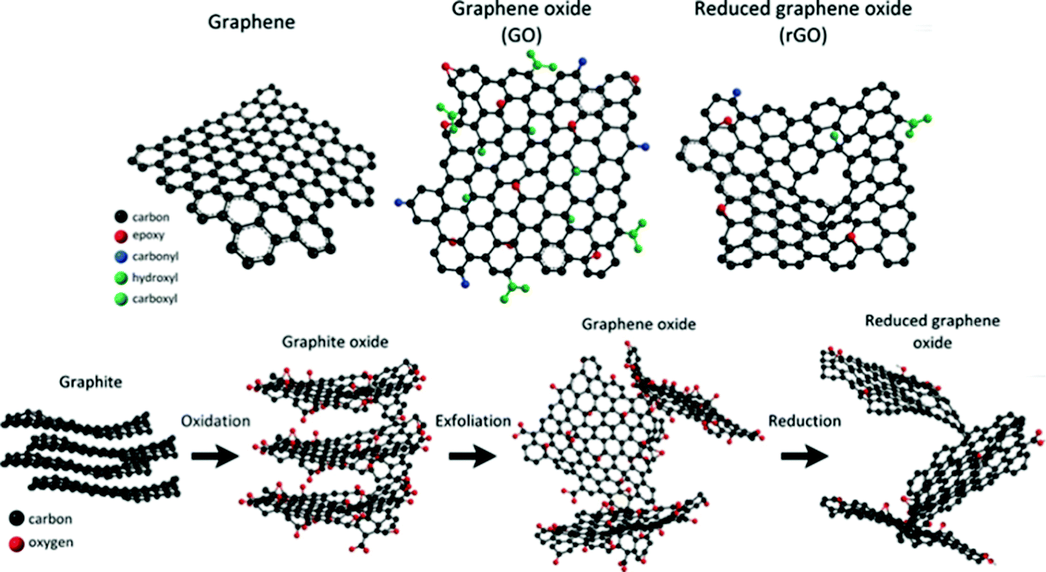
Graphene, a two-dimensional monolayer of sp2-bonded atoms, has been considered as a promising sensing material due to its large specific surface area and extremely high electron mobility. Especially, owing to its 2D structure, every carbon atom is a surface atom which can be sensitive to adsorbed molecules. Graphene can be prepared by using physical or chemical methods. In its initial preparation stage, graphene was synthesized by mechanical exfoliation. Afterwards, due to the inefficiency of mechanical exfoliation, the epitaxial growth method46 and chemical vapor deposition method47 were adopted; however, the required high temperature or ultrahigh vacuum conditions could limit its practical application. Subsequently, as a derivative of graphene, graphene oxide (GO) with oxygen functional groups became a potential gas-sensing material, and it was prepared by the Hummers' method.48 However, GO is an electrically insulating material that cannot be directly used for gas sensing. To address this issue, reduced graphene oxide with conductivity can be obtained through using various reduction methods, including thermal reduction49 and chemical reduction,50–52 as shown in Fig. 1.
 |
| | Fig. 1 Schematics of the chemical structures of graphene, graphene oxide, and reduced graphene oxide; route of graphite to reduced graphene oxide. Reproduced from ref. 45 with permission from American Chemical Society. | |
4.1.2 Graphene-based chemiresistive-type gas sensors.
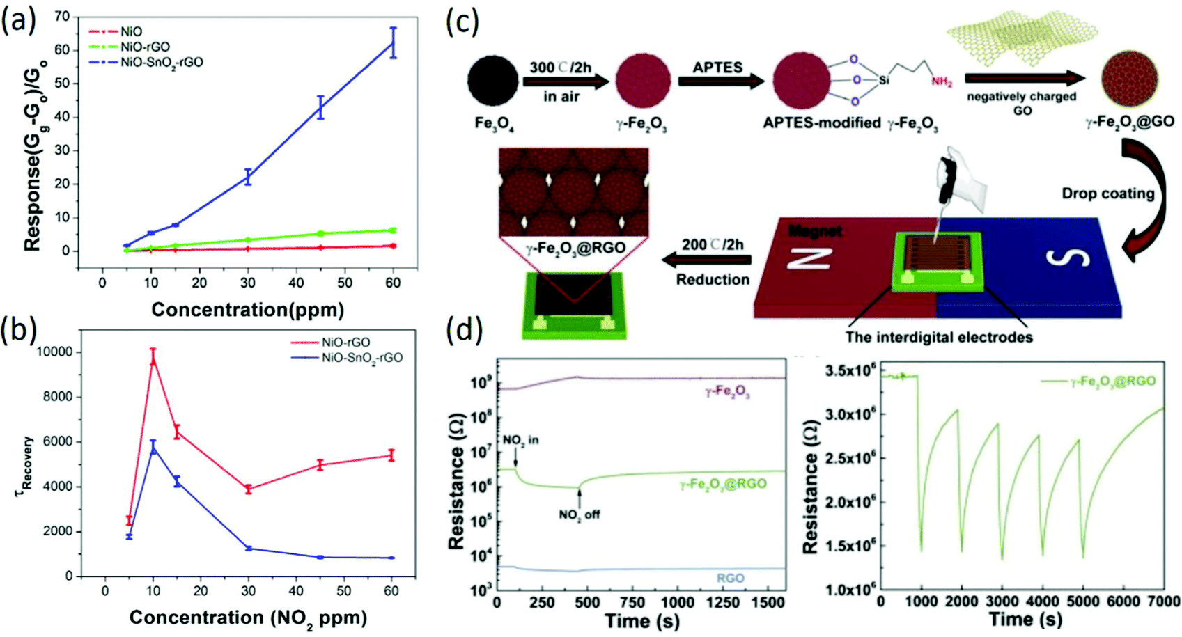
Because of their large specific surface areas for molecule adsorption and outstanding electrical properties with low noise level and high carrier mobility, graphene-based materials have received great attention for gas sensing, especially for chemiresistive-type sensors. To meet the requirements of gas detection in practical applications, graphene-based sensing materials have undergone a long change from bare graphene to graphene-based ternary nanocomposites. Initially, mechanically exfoliated graphene prepared by Novoselov et al.53 was employed for gas sensing, and it exhibited a limit of detection down to parts per billion. According to the Hall measurements of graphene sensors, it was confirmed that gas-induced changes in resistivity had different magnitudes for different gases, in which the donor characteristics of NH3, CO, and ethanol were confirmed as well as the acceptor characteristics of NO2, H2O, and I2. Inspired by this work, extensive theoretical and experimental research of graphene-based sensors was processed. Using first-principles calculations,54 the optimal adsorption positions and orientations of various types of molecules on defective and functionalized graphene54–56 were determined and the adsorption energies were also calculated, which could be helpful for the elaboration of the charge transfer mechanism and the improvement of sensing properties in graphene-based gas sensors. Afterwards, reduced graphene oxide (rGO) prepared by low-temperature solvent thermal reduction49 or chemical reduction50,57 was used for gas sensing, and it also presented excellent sensitivities to gas molecules. To further improve the sensing properties of bare rGO-based gas sensors, rGO composited with the second phase was widely reported, such as carbon nanotubes58 and conductive polymers.59 Especially, rGO decorated with various metal oxides was widely reported to enhance the sensing properties, including SnO2,60,61 WO3,62,63 NiO,64 ZnO,65 In-doped SnO2,66 In2O3,67 which exhibited largely enhanced sensing properties compared to the bare rGO or the bare metal oxide due to the formation of heterojunctions and increased active sites for gas adsorption. Recently, ternary nanocomposites were also prepared for gas sensing. For instance, rGO–SnO2-multiwalled carbon nanotubes prepared by a hydrothermal method exhibited enhanced room-temperature NO2 sensing performance compared to rGO–SnO2 sensors.68 Moreover, in our previous work, NiO–rGO composited with SnO2 was successfully prepared for gas sensing;1 it exhibited a remarkably higher response to NO2 at room temperature with a fast response/recover rate, and the response of the ternary nanocomposites to 60 ppm NO2 was 10 times larger than that of NiO–rGO under the circumstance of a nearly equal specific surface area (Fig. 2a and b), indicating the important role of the heterojunction and the formation of C–O–Ni interface bonds. Although demonstrations of improvement in the room-temperature sensing performance of graphene-based nanocomposites are numerous, the sensing chips fabricated based on the drop-casting method can hardly maintain repeatable sensing properties. To solve this problem, uniform 3D Fe2O3-@rGO core–shell films were deposited by magnetic-field-assisted drop-coating,69 as shown in Fig. 2c; this approach solves the coffee ring effect problem caused by the drop-coating method, exhibiting excellent sensitivity, selectivity and repeatability (Fig. 2d).
 |
| | Fig. 2 (a) Comparison of the sensitivity of as-prepared samples to different concentrations of NO2. (b) Time constants of the recovery curves of NiO–rGO and NiO–SnO2–rGO at different NO2 concentrations. Reproduced from ref. 1 with permission from Elsevier. (c) The fabrication procedure of γ-Fe2O3@RGO-based sensing devices. (d) The changes of the sensor resistance values of γ-Fe2O3, γ-Fe2O3@RGO, and RGO towards 50 ppm NO2, respectively; the response repeatability of the γ-Fe2O3@RGO sensor when exposed to 50 ppm NO2. Reproduced from ref. 61 with permission from Elsevier. | |
4.1.3 Graphene-based FET-type gas sensors.
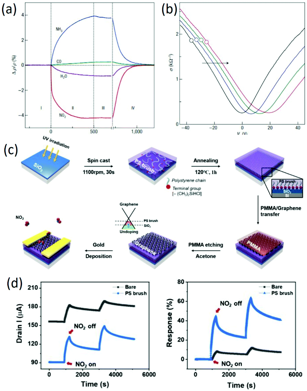
Because graphene is an exceptionally low-noise material electronically, graphene-based FET sensors were firstly adopted by F. Schedin et al.70 for detecting individual gas molecules. The adsorbed molecules change the local carrier concentration in graphene by one electron at a time, leading to step-like changes in resistance. In addition to the changes in resistance aroused by gas adsorption (Fig. 3a), the increased gas exposure shifted the V-shaped (Vg) curves as a whole, and the curves became broader around the neutrality point (Fig. 3b). Together with the unaffected Hall-effect mobility, the lack of significant changes in their shape and the parallel shifts prove that the gas adsorption did not affect the scattering rate. Therefore, the detection of gas molecules by using graphene FET sensors was mainly based on the changes in conductivity, which were caused by carrier doping. In this study, it is worth noting that the adsorbed molecules were strongly attached to the graphene devices at room temperature, which cannot be recovered unless annealed in vacuum. Recently, TiO2/graphene hybrid FET sensors with varied hybrid areas were used for NH3 sensing, which can maintain superior sensing and recovery performance simultaneously through a switch in the sensing mode via gate biasing, attributed to the Coulomb interactions between the charged polar donor molecules and positively polarized surface.71 In other work, to further improve the sensing properties of graphene-based FET sensors, surface modification layers of a silicon substrate were employed to reduce any unintentional doping by screening the charged impurities.72Fig. 3c shows the fabrication process of PS brush-modified graphene FETs. After insertion of a polystyrene (PS) brush, reduced doping of graphene on the PS brush leads to a low base current at Vg = 0 V, and the current increase upon NO2 exposure is higher in the graphene/PS brush (Fig. 3d). Additionally, the hole mobility of the graphene on the PS brush is around 3.5 times higher than that of graphene on the bare SiO2 substrate, leading to a faster response to gas molecules. Moreover, graphene FETs on the PS brush exhibited a lower limit of detection (LOD) compared to the graphene FETs on the bare substrate, attributed to the reduced doping of graphene by blocking charged impurities on SiO2/Si with a PS brush interlayer. This study indicated that the control of substrate-induced doping of graphene is a direct method to improve the sensing properties of graphene-based FETs.
 |
| | Fig. 3 (a) Changes in resistivity caused by exposure of graphene to various gases. (b) Constant mobility of charge carriers in graphene with increasing chemical doping. Reproduced from ref. 70 with permission from Nature Publishing Group. (c) Schematic of the fabrication of PS brush-modified graphene FETs. (d) Dynamic gas sensing properties of bare graphene and PS brush-modified graphene FETs. Reproduced from ref. 72 with permission from American Chemical Society. | |
4.1.4 Summary of graphene-based gas sensors.
As described before, graphene has received great attention in chemiresistive-type and FET-type gas sensors, which all exhibit superior sensing properties. For graphene-based chemiresistive-type gas sensors, although the theoretical demonstration of selective gas adsorption of N-doped or Al-doped graphene has been reported, practical preparation of such sensors has still not been revealed to date. Therefore, the poor selectivity problem is a long-standing issue. Besides, graphene is mostly employed in substrate materials to composite with other sensing materials due to the existence of functional groups, the large specific surface area and the higher electron mobility, leading to enhanced sensitivity of the nanocomposites compared to their single phase sensing materials. However, the sensing properties of graphene-based chemiresistive-type sensors should be further improved, such as excellent selectivity, lower limit of detection, and higher sensitivity. To attain this goal, the precise control of the distribution and amount of the second phase, the adoption of monolayer graphene or graphene oxide in nanocomposites, and functionalizing with specific functional groups could be future directions for graphene-based chemiresistive-type gas sensors. Compared with chemiresistive-type sensors, graphene-based FET-type sensors have demonstrated miniaturization and ultralow power consumption with V-shaped conductivity profiles. Especially, together with the pre-bias effect, multi-parameters such as threshold swing, threshold voltage, and electron mobility offer an effective tool to distinguish mixture gases. However, graphene-based FET-type sensors are still in their infancy owing to their tedious fabrication processes, slow recovery rates, lower sensitivity, etc.; this could be addressed by integration of graphene and sensing devices, substrate or surface modification, and introduction of an external light source.
4.2 2D TMDs
4.2.1 Structure and synthesis method of 2D TMDs.
TMDs have a layered structure with the general chemical formula of MX2, where M is a transition metal element (e.g., Mo, W, V, Nb) and X stands for a chalcogen (e.g., S, Se, Te). Commonly, monolayer TMD is composed of three atomic layers, in which a transition metal layer is sandwiched between two chalcogen layers. Depending on the different coordination models between M and X atoms or the stacking orders between layers, different crystal structures of MX2 can be formed, including 2H, 1T, 1T′, and 3R73 (Fig. 4). Among them, the 2H and 1T phase structures are the most reported for various applications, corresponding to the semiconducting phase and metal phase. Moreover, the phase structures can be transformed into each other under external conditions, such as strain or high pressure. On the basis of the layered structure of TMDs, the synthesis method of 2D TMDs can be divided into two categories: top-down and bottom-up methods. The top-down methods include mechanical exfoliation, mechanical force-assisted liquid exfoliation, and ion intercalation-assisted liquid exfoliation, which are mainly based on the exfoliation of thin layer 2D crystals from layer bulk crystals. In contrast, bottom-up methods include CVD growth and wet-chemical synthesis, which are dependent on chemical reactions of certain precursors at specific experimental conditions.
 |
| | Fig. 4 Crystal structures of MoS2 with different polymorphisms. Reproduced from ref. 73 with permission from American Chemical Society. | |
4.2.2 2D TMDs-based chemiresistive-type gas sensors.
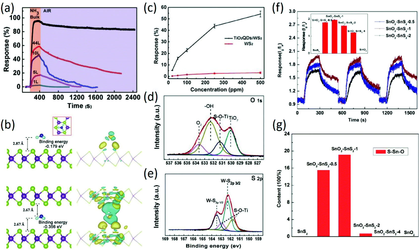
TMDs prepared by different methods, such as mechanical exfoliation, ion insertion-assisted exfoliation, and wet synthesis, have been widely used for gas sensing due to their atomic thin layer structures with large numbers of active sites. The reactive gaseous species adsorb on the surface of the sensing material, thus changing its resistance through surface–gas analyte interactions and the charge transfer process. In our previous work,74 different layer WS2 nanosheets prepared using a lithium–ion intercalation method were used for room temperature NH3 sensing. Although the response values decreased slightly with decreasing layer number of WS2, the room temperature recovery rate of monolayer WS2 rapidly and linearly shortened as the number of layers decreased (Fig. 5a), exhibiting potential application in room-temperature NH3 sensing. Especially, the fast recovery rate of monolayer WS2-based sensors is well-explained by using first-principles calculations, which indicated different binding energies between NH3 and the surface (−0.179 eV) or interlayer (−0.356 eV) of layered WS2 (Fig. 5b), contributing to the different recovery rates of WS2 sensors with different layer numbers. To improve the room-temperature NH3 sensing properties of WS2, WS2 decorated with TiO2 QDs was prepared by a wet-chemical synthesis method; it exhibited largely enhanced sensitivity to NH3 at room temperature, as shown in Fig. 5c, attributed to the effective electron transfer between WS2 and TiO2 QDs through S–O–Ti bonds, which was confirmed by XPS analysis (Fig. 5d and e). Moreover, the prepared nanocomposites exhibited long-term stability, showing no decline in sensitivity after several testing cycles.75 In another study, rGO composited with WS2 prepared by a one-step hydrothermal method was also employed for room-temperature NH3 sensing; the composite exhibited excellent sensitivity, selectivity and stability to 10–50 ppm NH3 at room temperature. The authors attributed the enhanced sensitivity to the introduced hydroxyls by rGO nanosheets and extra acid centers induced by WS2 nanoflakes.76 In addition to NH3 sensing, ultrathin p-type WS2 nanosheets synthesized by hydrothermal and calcination processes were employed for NO2 sensing; the response of p-type WS2 sensors to 0.1 ppm NO2 at room temperature is 9.3%, attributed to the ultrathin nanostructure and the rough surface of the WS2 nanosheets.77 Recently, p-type WS2 nanosheets prepared by sulfurization of WO3 nanomesh were employed to detail the different sensing mechanism of WS2 nanosheets for NO2 and H2S sensing. It was found that WS2 nanosheets do not require oxygen for NO2 sensing, while oxygen is essential for H2S sensing. This study based on the effect of oxygen content on the sensing properties of WS2 nanosheets is of great significance for the application of sensors in different environments.78 In addition, 2D WSe2 has shown increasing potential in NO2 sensing. On the basis of first-principles calculations, the electronic properties of monolayer WSe2 can be regulated by NO2 adsorption,79 which exhibits good prospects for NO2 sensor applications. For instance, WSe2 nanosheets prepared by a sonication-assisted exfoliation method using NMP as a dispersant were used for NO2 sensing; they exhibited a low experimental LOD of 50 ppb with a high sensitivity of 5.06, which is superior to many TMDs-based gas sensors at room temperature, attributed to the larger specific surface area of 2D WSe2.80 In addition to the commonly reported TMDs, other TMDs, including SnSe2, SnS2, and NbSe2, have been adopted for gas sensing applications. In our previous work, scalable SnS2 nanosheets composed of 1–3 layers were prepared by chemical exfoliation, which exhibited enhanced room-temperature NH3 sensing properties. Especially, the response time of the as-prepared SnS2 sensor (16 s for 500 ppm NH3) is the shortest among all the TMDs-based room-temperature NH3 sensors, attributed to the effective NH3 adsorption on the high energy defect sulfur vacancies of 2D SnS2.81 Subsequently, SnO2–SnS2 hybrids synthesized by the oxidation of SnS2 at 300 °C with different times exhibited high response to NH3 at room temperature (Fig. 5f). Moreover, it was found that the response of hybrids to NH3 at room temperature exhibited a strong dependence on the amount of interfacial bonds (Fig. 5g). The increased amount of interfacial bonds led to a higher response of the hybrid to NH3 at room temperature.82 Similarly, the SnSe2 thin film prepared by a thermal evaporation method with a portion of SnSe on its surface was employed for NO2 sensing. It was found that the constructed SnSe–SnSe2 heterostructure exhibited a response of 112% to 5 ppm NO2 at room temperature with fast response and recovery rates.83 Although the reports of TMDs-based gas sensors are numerous, further improvement in the sensing properties of 2D TMDs, including selectivity, sensitivity, and room-temperature recovery rate, are needed for their practical application.
 |
| | Fig. 5 (a) Response-recovery curves of WS2 nanosheets with different layers to 250 ppm NH3 at room temperature. (b) Configurations of NH3 adsorbed on single layer WS2 and in the interlayer space of bulk WS2. Reproduced from ref. 74 with permission from Elsevier. (c) The responses of nanocomposites and bare monolayer WS2 as a function of NH3 concentration. XPS spectra of O 1s (d) and S 2p (e). Reproduced from ref. 75 with permission from Elsevier. (f) Repetitive dynamic response–recovery curves of SnO2–SnS2 nanocomposites with different molar ratios. (g) Semi-quantitative analysis of the fraction of O–Sn–S among the total of O–Sn–O, O–Sn–S, and O–Sn. Reproduced from ref. 82 with permission from American Chemical Society. | |
4.2.3 2D TMDs-based FET-type gas sensors.
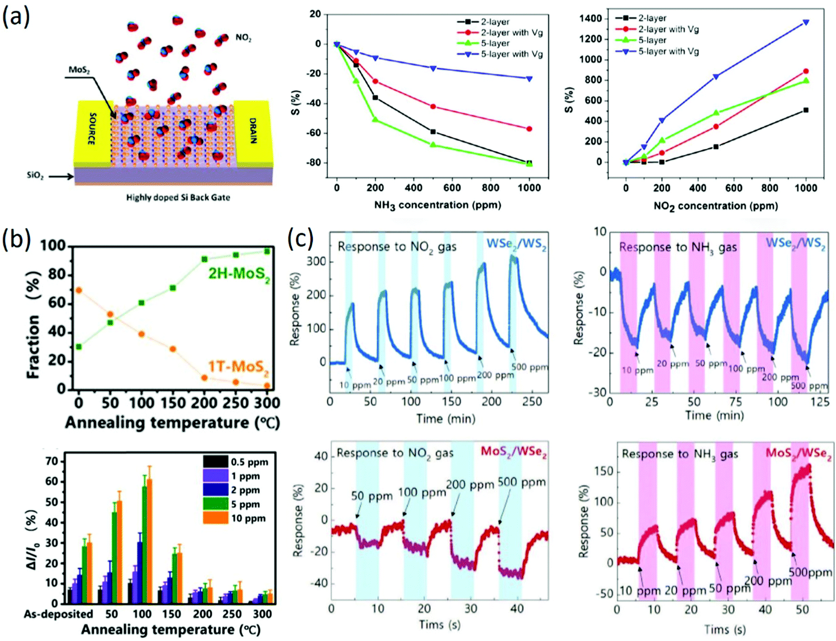
Due to their atomic layer structures with larger specific surface areas and higher carrier mobility in FET-type electronic devices, 2D TMDs have also received great attention in the FET-type gas sensing field. For instance, two-layer and five-layer MoS2 prepared by mechanical exfoliation were firstly adopted for FET-type gas sensing, and the device structure of the FET-type sensors is shown in Fig. 6a. It was found that the response of five-layer MoS2 to NH3, NO2 and water vapor was higher than that of two-layer MoS2 (Fig. 6a), and the selectivity of MoS2-based FET-type gas sensors was also enhanced by tuning the gate voltage and introducing an extra light source. The authors attributed the different sensitivities to the surface charge transfer between the MoS2 and gas molecules.84 Besides, monolayer MoS2 prepared by CVD growth was employed for FET-type gas sensing, and the fabricated FET-type sensors could detect 20 ppb NO2 and 1 ppm NH3 at room temperature. It was believed that the sensing properties were determined by the Schottky barrier height.85 Similarly, multi-layer MoS2 prepared by the CVD method also exhibited stable sensing properties to 1.2 ppm NO2, and the effect of electrode resistance on the gas sensing properties was also detailed by using a graphene electrode instead of a Au/Ti electrode.86 Afterwards, the sensing properties of MoS2-based FET-type sensors were enhanced by optimizing the layer number, bias voltage, gate voltage, channel dimension and substrate.87 Despite this, the sensitivity of bare MoS2 based FET-type sensors is still facing challenges of higher sensitivity and excellent selectivity due to limitations in the intrinsic properties of bare MoS2. To improve the sensing properties of MoS2-based FET-type sensors and enlarge their detection range, deposition of metal nanoparticles (Ag, Au, Pt, Pd, Sc, and Y) prepared by e-beam evaporation was employed as a kind of modifier to investigate the effect of the work function of the metal nanoparticles on the threshold voltage and conduction type of FET-type devices. It was found that the doping level increased with increasing work function of the metal nanoparticles, and the doping effect was largely enhanced by reducing the layer number of 2D materials. In addition, it was confirmed that potential room-temperature H2 detection can be attained by Pd decoration.88 Recently, to further improve the sensitivity of MoS2-based FET-type gas sensors, surface molecule modification,89 constructing heterostructures with different phase structures90 or different components91 has been widely reported. For instance, optimal molecule decoration with tetrafluorotetracyanoquinodimethane (F4TCNQ) on the surface of gold-assisted exfoliated large-scale thin MoS2 was realized by thermal deposition.89 The response of F4TCNQ-modified MoS2 was greatly improved by two or three orders of magnitude under all ranges of NH3 concentration, and the main mechanism for the enhanced sensitivity could be attributed to effective charge transfer due to band alignment among the heterogeneous structure. More importantly, it was concluded that organic molecules with similar chemical properties to F4TCNQ can also effectively improve the sensing properties of MoS2-based FET-type sensors. In another work, temperature-modulated 1T/2H heterophase in lithium-exfoliated nolayer MoS2 was prepared for FET-type gas sensing, and it exhibited a p-type semiconducting characteristic with the highest responsivity of 25% to 2 ppm NO2 and the shortest response of 10 s when the ratio of 1T to 2H was 0.6790 (Fig. 6b). Heterostructures with different components were also reported for gas sensing, in which p-type WSe2/WS2 gas sensors exhibited selectivity to NO2 gas and n-type MoS2/WSe2 gas sensors exhibited a higher response to NH3 than to NO2, as shown in Fig. 6c. It was also found that the exposed surface plays the most dominant role in transferring the charges from the gas, while the underneath layer could affect the responsivity depending on the type of heterostructure materials and the exposed gas.91 Although the sensing properties of 2D TMDs-based FET-type gas sensors was improved to some extent through optimization of the electronic device parameters, metal nanoparticle decoration, constructing heterostructures and organic molecule modification, many drawbacks also exist that need to be solved for the practical application of these sensors, such as surface charge transfer mechanism-induced poor selectivity, slow recovery rate, humidity-dependence, and instability after repeated use.
 |
| | Fig. 6 (a) Schematic of MoS2 transistor-based gas sensing devices; sensitivity as a function of concentration for two-layer and five-layer MoS2 nanosheets to NH3 and NO2. Reproduced from ref. 84 with permission from American Chemical Society. (b) Relative fractions of 1T and 2H phases as a function of temperature; relative current response of MoS2 to NO2 gas. Reproduced from ref. 90 with permission from American Chemical Society. (c) Consecutive gas sensing measurements of WSe2/WS2 and MoS2/WSe2 to NO2 and NH3, respectively. Reproduced from ref. 90 with permission from John Wiley & Sons, Inc. | |
4.2.4 Summary of 2D TMDs-based gas sensors.
With the development of TMDs-based chemiresistive-type gas sensors, 2D TMDs have been widely used for gas sensing, from layer number modulation and evolution of the exfoliation method to constructing nanocomposites with a second phase. All of these methods aim to improve the sensing properties of 2D TMDs, including the recovery rate, selectivity and sensitivity. In spite of this, the sensing properties of 2D TMDs should be further improved to meet the higher requirements in the extremely low concentration gas mixtures. Moreover, the sensing mechanisms of nanocomposites with enhanced sensing properties should be more detailed rather than the synergistic effect of the constituents, which could offer a guideline to further improve the sensing properties. Considering the excellent optoelectronic properties of 2D TMDs, the photovoltaic effects induced by self-powered TMDs-based chemiresistive gas sensors could be future directions to reduce power consumption. Compared with TMDs-based chemiresistive-type sensors, FET-type gas sensors based on 2D TMDs are attracting increasing attention due to the intrinsic optoelectronic properties of 2D TMDs and the miniature size of the gas sensing devices, which exhibit vast potential in gas sensing fields. On the basis of reported research work, the effects of the layer number, work function, contact resistance and channel resistance should be more detailed. Besides, the humidity effect, the room-temperature recovery rate and the sensitivity should be comprehensively considered, which could be solved by encapsulation, the introduction of an extra light source or constructing an effective heterojunction with the screened second phase.
4.3 2D MXenes
4.3.1 Structure and synthesis method of 2D MXenes.
2D MXenes are a class of layered transition metal carbides and/or nitrides that are produced from bulk MAX phases, where M is the transition metal (e.g., Ti, V, Cr, Nb, etc.), A is an A-group element (mostly IIIA or IVA), and X is either C or N. The MAX phases have a layered, hexagonal structure, in which M layers are nearly hexagonally close-packed together and X fills the octahedral sites, as shown in Fig. 7a.92 It should be noted that A is commonly metallically bonded to the M elements and interleaved in Mn+1Xn layers with stronger metallic bonding, making it impossible to exfoliate MAX phases into ultrathin 2D materials. Therefore, MXenes with three different structures (M2X, M3X2, and M4X3) are usually prepared by selectively etching the A layer followed by exfoliation methods (Fig. 7b). In a typical process, a powder of a MAX phase is immersed and stirred in aqueous HF solution for selective etching of A layers without disrupting the M–X bonds; then, ultrathin 2D MXenes can be obtained by sonication of the intermediate product in solution. However, not all of the MAX phases can be exfoliated into ultrathin MXenes, and the commonly used etching agent is a strong corrosive chemical (HF) that should be replaced by safer etching agents.
 |
| | Fig. 7 (a) Atomic and crystal structure MAX phases. Reproduced from ref. 91 with permission from American Chemical Society. (b) Schematic of the Ti3C2Tx synthesis procedure. Reproduced from ref. 93 with permission from American Chemical Society. | |
4.3.2 2D MXenes-based chemiresistive-type gas sensors.
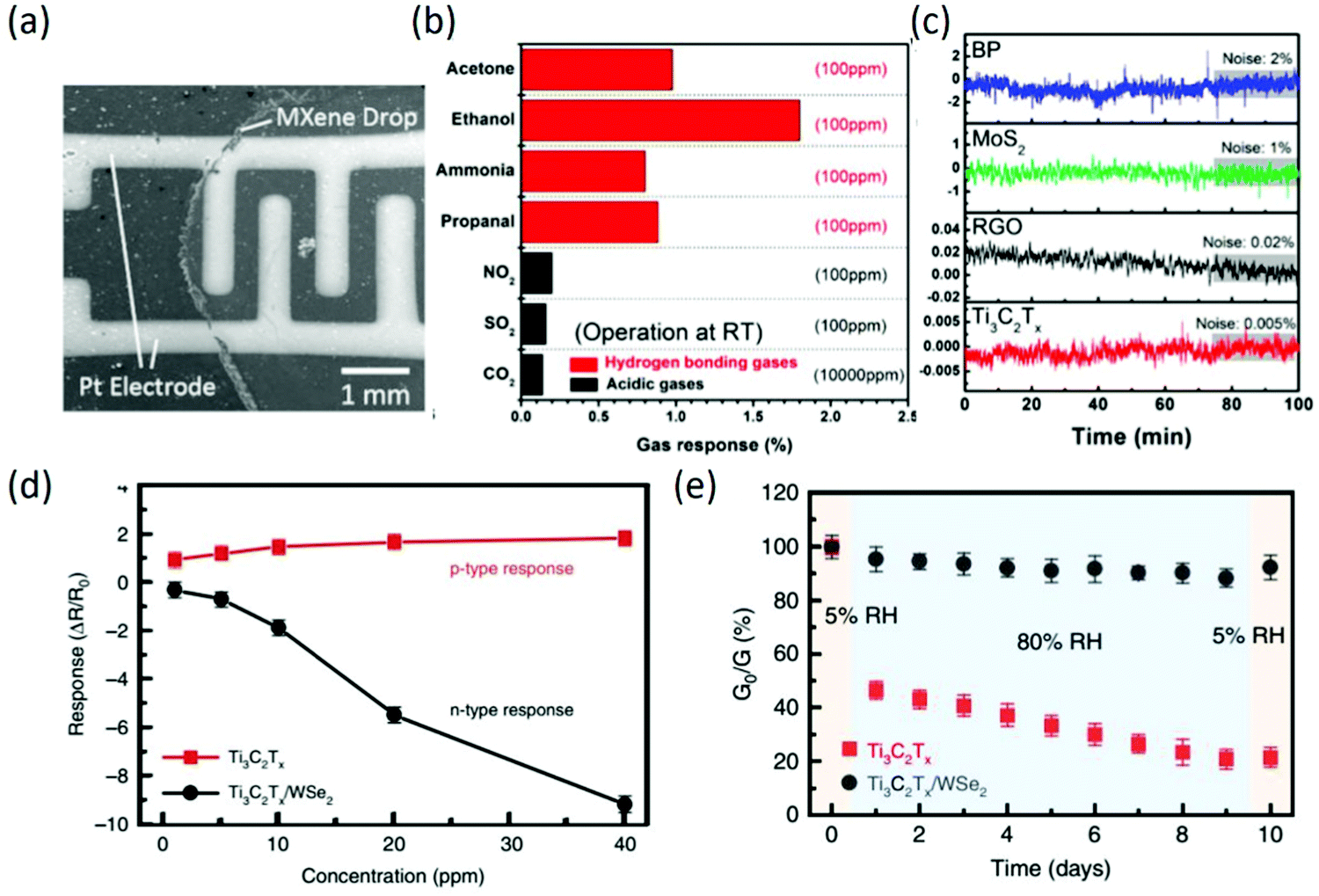
Since the discovery of MXenes in 2001, many kinds of MXenes have been successfully prepared. Among them, Ti2CTx has been suggested to have potential for sensing different gases, such as NH3, based on theoretical studies.93 Afterwards, Ti3C2Tx was firstly reported for volatile organic compound (VOC) sensing; it was synthesized by removal of Al atoms from Ti3AlC2 and integrated on flexible polyimide platforms. Moreover, the as-fabricated Ti3C2Tx sensors can measure ethanol, methanol, acetone, and ammonia gas at room temperature and show p-type sensing behavior. The probable sensing mechanism was also proposed in terms of the majority charge carrier transfer between the sensing material and gas species, and the device structure of the as-fabricated chemiresistive-type sensors is shown in Fig. 8a.94 Owing to the fully covered functional groups and the metallic conductivity behavior, Ti3C2Tx sensors exhibited high selectivity toward hydrogen-bonding gases over acidic gases (Fig. 8b), and the empirical low limit of detection (LOD) of 50 ppb and the theoretical LOD in the sub-ppb level for VOC gases are the lowest of any gas sensors based on 2D materials operating at room temperature. Especially, the signal-to-noise ratio of Ti3C2Tx sensors was up to 2 orders of magnitude higher compared to that of all other 2D materials, as shown in Fig. 8c. Interestingly, Ti3C2Tx sensors displayed a positive variation of resistance regardless of the type of gases (reducing or oxidizing gases), indicating that the charge carrier transport of the channel was always hindered when a gas molecule was adsorbed, which exhibited a different sensing mechanism compared with common semiconducting materials.95 In addition to Ti3C2Tx sensors, delaminated single-/few-layer V2CTx sensors with ultrahigh sensitivity toward nonpolar gases were also demonstrated; they can detect both polar and nonpolar chemical species, including hydrogen and methane, with very low limits of detection of 2 and 25 ppm at room temperature, attributed to the surface oxygen functional groups on the surface of V2CTx flakes.96 In recent years, MXenes have still received great attention in the gas sensing field. To further meet the requirements in practical application, MXenes-based nanocomposites have been widely been reported for gas sensing, including Ti3C2Tx/TMDs and Ti3C2Tx/graphene. For instance, Ti3C2Tx/WSe2 hybrid sensors were prepared by liquid phase exfoliation and a subsequent inkjet printing method; they exhibited an over 12-fold increase in ethanol sensitivity compared to pristine Ti3C2Tx sensors due to the numerous heterojunction interfaces formed between Ti3C2Tx and WSe2 (Fig. 8d). Moreover, the hybridization process provided an effective strategy against MXene oxidation by restricting the interaction of water molecules (Fig. 8e) from the edges of Ti3C2Tx.97 In other work, Ti3C2Tx MXenes/graphene hybrid fiber prepared by a scalable wet-spinning process exhibited significantly improved NH3 gas sensitivity at room temperature due to the optimized band gap, synergistic effect, and increased oxygen in the MXene terminal atom of hybrid fibers.98 To improve the stability of MXene sensors in a humid environment, a surface functionalization strategy for Ti3C2Tx with fluoroalkylsilane (FOTS) molecules was demonstrated, which not only exhibited mechanical and environmental stability but also enhanced sensing performance. According to density functional theory simulations, the strong adsorption energy of ethanol on Ti3C2Tx-F and the local structure deformation induced by ethanol adsorption contribute to the gas sensing enhancement.99 Besides, the gas detecting range was enlarged by incorporating Pd colloidal nanoclusters into Ti3C2Tx nanosheets, which displayed moderate H2 response at room temperature; this was attributed to strong H2 adsorption in the lattice of ultrafine Pd nanoclusters, which altered the work function and then induced electron doping of the MXene.100
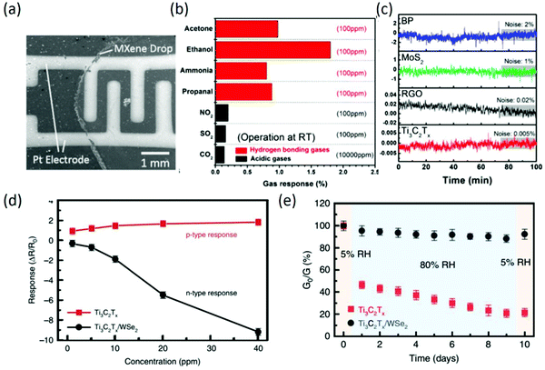 |
| | Fig. 8 (a) Scanning electron microscopy image of an MXene film deposited on an interdigitated platinum electrode by drop casting. (b) Gas response performance of Ti3C2Tx sensors upon exposure to various gases. (c) Electrical noise of sensors during N2 exposure. Reproduced from ref. 95 with permission from American Chemical Society. (d) Comparison of gas response as a function of ethanol gas concentration for Ti3C2Tx and Ti3C2Tx/WSe2 sensors. (e) Changes in electrical conductance of pristine Ti3C2Tx and Ti3C2Tx/WSe2 sensors under alternative RHs of 5% and 80% over 10 days. Reproduced from ref. 97 with permission from Nature Publishing Group. | |
4.3.3 2D MXenes-based FET-type gas sensors.
To date, MXene-based FET-type gas sensors have been rarely reported, possibly due to their metallic features. Although pure MXenes are regarded to be theoretically metallic, their metallic properties have been reported to be transformed into semiconductive with surface functional terminations that possess high field-effect electron mobility. Therefore, MXenes can also be used as a promising material in FET-type sensing platforms. For instance, FET was fabricated with a single/double-layer Ti3C2Tx MXene, which exhibited a fast (∼1 s), sensitive, and selective response to alkali with high anti-interference ability in a high-ionic-strength environment.101 Besides, considering their water dispersibility, high conductivity, and work-function tunability, 2D MXenes have potential for application as high-performance and low-cost electrodes in FET devices.102 It was reported that the work function of Ti3C2Tx MXene electrodes can be effectively modulated via chemical doping with NH3, and FET chips fabricated with Ti3C2Tx MXene electrodes showed excellent device performance, exhibiting potential application in gas sensing fields.103
4.3.4 Summary of 2D MXenes-based gas sensors.
As described before, 2D MXenes exhibit great potential in gas sensing fields due to their metallic properties with various functional groups. However, 2D MXenes are usually sensitive to humidity and are not very stable at elevated temperature, which poses great challenges for gas detection in a harsh environment and the following post-treatment of MXene materials. Therefore, more emphasis should be placed on the stability of MXenes, such as controlled surface terminations, selective modification of the functional groups, and adoption of novel synthetic materials. Moreover, functionalization of terminal groups with electron-withdrawing groups or electron-donating groups could be an effective method to improve the selectivity of MXene-based chemiresistive-type sensors. Besides, on the basis of density functional theory calculations, not only have reactive MXenes been confirmed for gas adsorption, but the selectivity of MXenes can also be improved upon oxygen functionalization. For instance, Mo2CO2 and V2CO2 exhibited good selectivity to NO molecules, while Nb2CO2 and Ti2CO2 showed good selectivity toward NH3, indicating that oxygen-functionalized MXenes are potential materials for gas sensing.104 Therefore, in addition to the most commonly reported Ti3C2Tx in the 2D MXenes family, other kinds of 2D MXenes with or without functionalization should be considered for gas sensing, which could exhibit promising gas sensing properties for practical application. As for FET-type gas sensors, MXenes have rarely been reported for gas sensing due to their intrinsic metallic properties. However, theoretical predication of semiconducting properties in 2D MXenes was reported and awaits experimental verification. Afterwards, together with the metallic MXene electrode, the heterostructure-based FET-type gas sensors composed of metallic MXenes and semiconducting MXenes with lower contact resistance could exhibit excellent sensing properties.
4.4 2D Phosphorene
4.4.1 Structure and synthesis method of 2D phosphorene.
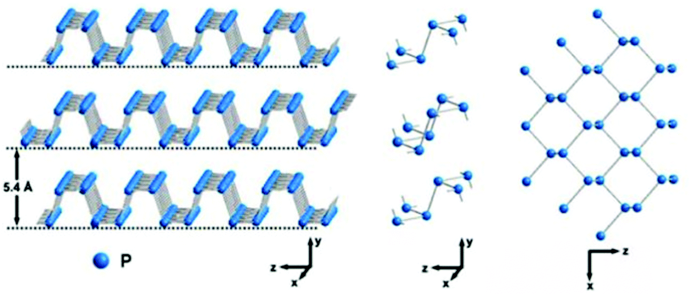
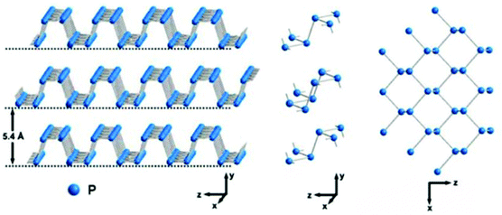
Phosphorene is a monolayer of black phosphorus (BP) with a puckered honeycomb structure. Bulk BP has a layered orthorhombic crystal structure whose interlayer distance is 5.4 Å. In a single layer (Fig. 9), each P atom is covalently bonded with three adjacent atoms to form a puckered honeycomb structure. Among the four P atoms, three of them are in the same plane, while the fourth one is located at the parallel adjacent plane.105 In 2014, BP crystals were firstly prepared by using red phosphorus as the source under high pressure and temperature conditions.106 Afterwards, few-layer BP was fabricated by the mechanical exfoliation method from the bulk BP crystals. Currently, liquid exfoliation and CVD methods are also employed to prepare layered BP for various applications because of its tunable direct bandgap, high carrier mobility and high current on/off ratio as well as its anisotropic electrical, optical, and thermal properties.
 |
| | Fig. 9 Crystal structures of BP. Reproduced from ref. 73 with permission from American Chemical Society. | |
4.4.2 2D Phosphorene-based chemiresistive-type gas sensors.
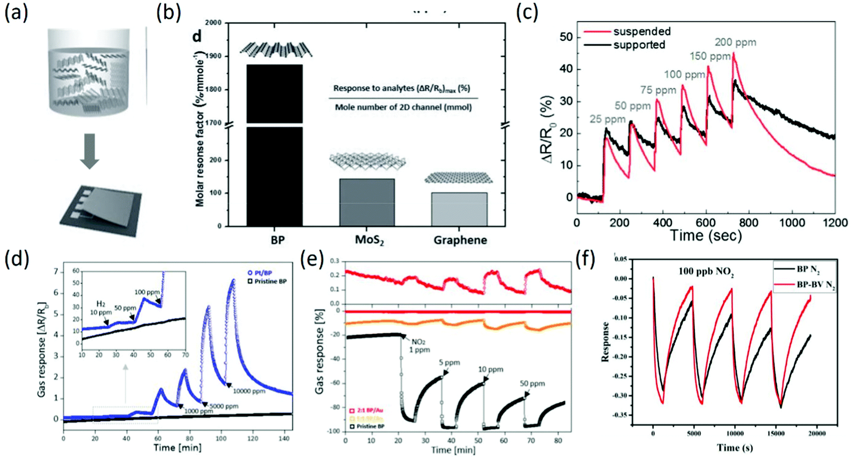
Considering the potential application of BP in gas sensing fields, a systematic study on the adsorption of small molecules (CO, H2, H2O, NH3, NO, NO2 and O2) on phosphorene was detailed on the basis of dispersion corrected density functional theory, mainly focusing on the energetics, magnetic moments, and charge transfer between these molecules and phosphorene. It was found that CO, H2, H2O and NH3 act as charge donors, while NO2, NO and O2 serve as charge acceptors, which provides a reference for assessing the effect of physisorbed small molecules on phosphorene.107 Similarly, through first-principles calculations of the adsorption of CO, CO2, NH3, NO and NO2 gas molecules on monolayer phosphorene, the superior sensing performance of phosphorene was predicted, and the optimal adsorption positions of these molecules on the phosphorene were also determined.108 Afterwards, the excellent sensing performance of BP was experimentally confirmed by accurately comparing the sensing properties (response/recovery time, selectivity, molar response factor, and adsorption behavior) of BP with those of MoS2 and graphene. Under identical liquid phase deposition methods (Fig. 10a), the calculated molar response factors, which reflect the intrinsic sensing capacity of each material with the same molecule number, are about 20 times higher than that of MoS2 and graphene (Fig. 10b). More importantly, only BP showed highly selective response to NO2 while being unresponsive to oxygen-functionalized molecules, whereas MoS2 and graphene had similar responses to all the chemical compounds.109 To increase the sensing performance of BP chemical sensors, floating BP flakes on top of an electrode were prepared to provide full (both sides) adsorption sites and avoid the interface scattering effect. It was found from Fig. 10c that the suspended BP sensors exhibited superior gas response (increased by 23%) with a faster desorption rate than the conventional supported BP gas sensors.110 To enlarge the detection range, BP incorporated with Au and Pt was investigated for gas sensing. After incorporation with Pt, the nanocomposites could detect low concentrations of H2 with higher response amplitude (Fig. 10d). Moreover, the incorporation of Au nanoparticles can induce the effect of n-doping on p-type pristine BP (Fig. 10e), that is, the response behavior of BP to oxidizing gas changed from a p-type response to an n-type response with high stability and a lower noise baseline.111 Recently, to further improve the sensing properties of BP-based gas sensors, BP nanosheets composited with the second phase have been widely reported.112,113 For instance, to overcome the limitations of BP-based sensors of slow recovery rate and fragile reproducibility to strongly oxidizing gases, few-layer BP nanosheets incorporated with benzyl viologen (BV) were prepared, and they exhibited superior recovery characteristics, repeatability, selectivity, and humidity-repelling features with nearly unchanged response (Fig. 10f). BV not only offered additional electrons to NO2 to compensate the loss of NO2 adsorption because of the surface coverage of BV, but also passivated BP through occupying high energy adsorption sites and then maintaining a reversible recovery and a repeatable response.114 In other work, 4-azidobenzoic acid was used to modify BP nanosheets to improve the stability of BP. After modification, the obtained Langmuir–Blodgett film through electrostatic interaction between modified BP nanosheets and dye molecules showed good sensitivity to acid and alkali gas, with higher stability after 10 cycles of acid-alkali testing.115
 |
| | Fig. 10 (a) Schematic of the chemical exfoliation of bulk BP and the device fabrication process. (b) The molar response factor is calculated and compared with that of MoS2 and the graphene channel to demonstrate the superior gas adsorption properties of BP. Reproduced from ref. 109 with permission from John Wiley & Sons, Inc. (c) Response of the supported and suspended BP chemical sensors to different NO2 concentrations in N2 atmosphere. Reproduced from ref. 110 with permission from Elsevier. (d) Gas response of Pt/BP and pristine BP toward various H2 concentrations. (e) Tunable gas response behavior of Au/BP achieved by controlling Au incorporation concentrations. Reproduced from ref. 111 with permission from American Chemical Society. (f) Repeatability of BP and BP-BV sensors to 100 ppb NO2. Reproduced from ref. 114 with permission from Elsevier. | |
4.4.3 2D Phosphorene-based FET-type gas sensors.
To ensure the stability of BP-based FET-type gas sensors, thick BP flakes were firstly employed for investigating the chemical sensing performance, and the corresponding device structure is shown in Fig. 11a. The BP FET sensors exhibited a clear conductance change in response to NO2 concentrations as low as 5 ppb (Fig. 11b), and the sensing devices owned good recovery to the original conductance after flushing the device with argon, suggesting reversible adsorption and desorption of NO2. Additionally, the relative conductance change followed the Langmuir isotherm (Fig. 11c) for NO2 molecules adsorbed on a surface, implying that NO2 molecule adsorption via site binding and charge transfer was the dominant mechanism for these BP FET devices. The systematic increase in conductance with increasing NO2 concentration suggests that NO2 molecules withdrew electrons and doped the BP flakes with holes.116 In other work, high-performance 2D phosphorene nanosheets (PNSs)-based FET sensors were also demonstrated (Fig. 11d); they exhibited ultrahigh sensitivity to NO2 in dry air, and the sensitivity was dependent on the thickness (Fig. 11e). When the thickness of PNS was 4.8 nm, the response to 20 ppb NO2 at room temperature could reach 190%. According to a statistical thermo-dynamic model with inputs from first-principles calculations, the highest sensitivity could be realized for PNS thickness ranging from 4.3 to 10 nm, which is consistent with experimental results, depending on the substrate quality. Additionally, the fabricated PNS sensors exhibited excellent stability in a dry air environment and high selectivity to NO2 gas (Fig. 11f) in the presence of H2, CO and H2S gases.117 However, various challenges, such as tedious fabrication, low response caused by rapid oxidation, large device variation due to poor control over the layer thickness, etc., still exist in BP-based FET-type sensors, which could be solved by selected-area exfoliation or correlating the on/off ratio with the sensitivity parameters.118
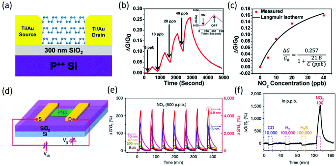 |
| | Fig. 11 (a) Device structure of a multilayer BP-based FET-type sensor. (b) Relative conductance changes vs. time in seconds for a multilayer BP sensor showing sensitivity to NO2 concentration. The inset shows a zoomed view of the response–recovery curves upon exposure to 5 ppb NO2. (c) The fitted Langmuir isotherm is agreement with the measure values. Reproduced from ref. 116 with permission from American Chemical Society. (d) Schematic of an FET device based on the PNS and the circuit for electrical and sensing measurements. (e) Thickness-dependent multi-cycle responses of the PNS sensor to 500 ppb NO2. (f) Dynamic sensing response curve of the 4.8 nm PNS to various gases, showing the excellent selectivity to NO2. Reproduced from ref. 117 with permission from Nature Publishing Group. | |
4.4.4 Summary of 2D phosphorene-based gas sensors.
On the basis of the above-described research work, 2D phosphorene exhibited even higher response and excellent selectivity to NO2 gas compared to graphene and MoS2, indicating that 2D phosphorene is also a promising 2D material for gas sensing. In spite of this, there is still much room for improvement of the sensing properties in 2D phosphorene-based chemiresistive-type sensors, including the recovery rate and sensitivity. Although the sensing properties of 2D phosphorene have been improved by effective device design and surface molecule modification, extensive strategies should also be adopted to further improve the sensing properties of BP. Considering the instability of the BP layer in an air environment, surface modification or encapsulation seems necessary. However, the extra modification will definitely reduce the number of active sites of BP for gas adsorption. Therefore, the sensitivity, the humidity effect, the gas adsorption–desorption, and the stability of BP-based chemiresistive-type sensors should be comprehensively considered. As for the BP-based FET-type gas sensors, the effect of the BP thickness on the sensing properties and the dominant mechanism of bare BP-based FET-type gas sensors were detailed, which all exhibited potential applications in gas sensing. Nevertheless, BP-based FET-type sensors are still in an early stage. For instance, BP-based nanocomposites have rarely been reported for FET-type sensing, in which suitable selection of the BP layer number could be very important for excellent gas sensing properties because the variance in layer number not only affects the sensing properties of bare BP as described above, but also leads to different energy band structures of BP that can form different types of heterostructures with the second phase, leading to different sensing properties of nanocomposites.
4.5 The other layered 2D material sensors
In addition to the above-introduced 2D materials, other layered 2D materials, such as layered semiconducting metal oxides and layered group III–VI semiconductors, have also exhibited potential application in gas sensing fields. 2D metal oxide nanosheets can be employed as active sensing elements both individually and when incorporated in 3D architectures. However, individual nanosheets are very difficult to handle for gas sensing; most reports employing 2D metal oxide nanosheets as sensing materials refer to 3D architectures that consist of 2D nanosheets. 2D metal oxide nanosheets are usually prepared by hydrothermal or solvothermal procedures, spontaneously or with the help of structure-directing agents, in which meso- and macropores can be formed during oxidation or annealing of non-porous precursor flakes. To date, various 2D metal oxides assembled in flower or film structures with different nanosheet thicknesses have been widely reported for gas sensing, including WO3, ZnO, SnO2, V2O5, NiO, and Co3O4, which exhibited higher sensing properties due to the large specific surface area and pore structure-induced gas diffusion channels.119 Recently, density functional theory calculations have been widely employed to study the sensing mechanisms of 2D metal oxides, including 2D WO3120 and noble metal-doped or decorated ZnO,121,122 at the atomic scale; this could provide atomistic insight and a better understanding of the sensing properties of 2D metal oxides, exhibiting the huge potential of 2D metal oxides in gas sensing. However, the reported 2D metal oxide-based gas sensors are almost all chemiresistive-type, while FET-type gas sensors based on 2D metal oxide nanosheets are rarely reported.
Layered group III–VI semiconductors, including GaS,123 GaSe,124 GaTe,125 and InSe,126 also exhibit potential application in gas sensors on the basis of the different photoelectric properties of fabricated phototransistors in various gas environments; they can be synthesized by mechanical exfoliation, liquid exfoliation, vapor-phase deposition, and van der Waals epitaxial growth methods. In addition to the common 2D TMDs, room-temperature NO2 sensing characteristics of 2D NbS2 nanosheets have also been reported. It was found that the fabricated NbS2 chemiresistive-type sensors exhibited reversible and selective NO2 sensing performance at room temperature, and the sensing properties of 2D NbS2 can be modified by different edge configurations depending on the synthetic conditions.127 In other work, 2D PtSe2 films prepared by a post-selenization process were employed for NO2 sensing. The sensing properties were further optimized by controlling the selenization temperature, and the layer number was also essential for the good sensing properties. Through comprehensive analysis, the important roles of the strain effect and band structure of PtSe2 films in the sensing properties were revealed.128 Beyond that, PtSe2-based FET-type sensors were reported; they exhibited very high responses of 2220% and 675% to 10 ppm and 1 ppm NO2, respectively, indicating the promising toxic gas detection by PtSe2 FET-type sensors.129 In addition to the above-described 2D materials, novel 2D materials such as SiBi nanosheets130 and lead pathalocyanine thin films131 were reported for gas sensing. Additionally, the sensing properties of 2D materials for chemiresistive- and FET-type gas sensing have been summarized, as shown in Table 2.
Table 2 Comparison of the sensing properties of 2D materials from previously reported studies on chemiresistive- and FET-type gas sensors
| 2D Materials |
Sensor type |
Gas |
Response |
LoT (ppb) |
Signal |
Ref. |
| Gr |
Chemiresistive |
1 ppm NO2 |
4% |
1 |
G |
53
|
| γ-Fe2O3@RGO |
Chemiresistive |
50 ppm NO2 |
3.43 |
<100 |
G |
69
|
| NiO–SnO2–rGO |
Chemiresistive |
60 ppm NO2 |
62.27 |
— |
G |
1
|
| PS modified Gr |
FET |
50 ppm NO2 |
45.1% |
4.8 |
G, VDirac |
72
|
| Monolayer WS2 |
Chemiresistive |
250 ppm NH3 |
2.58% |
— |
G |
75
|
| TiO2 QDs/WS2 |
Chemiresistive |
250 ppm NH3 |
43.72% |
— |
G |
75
|
| rGO–WS2 |
Chemiresistive |
10 ppm NH3 |
121% |
— |
G |
76
|
| Five-layer MoS2 |
FET |
200 ppm NH3 |
51% |
— |
G |
84
|
| Five-layer MoS2 with Vg |
FET |
200 ppm NH3 |
8% |
— |
G |
84
|
| Five-layer MoS2 |
FET |
100 ppm NO2 |
200% |
— |
G |
84
|
| Five-layer MoS2 with Vg |
FET |
100 ppm NO2 |
400% |
— |
G |
84
|
| CVD-grown monolayer MoS2 |
FET |
20 ppb NO2 |
20% |
— |
G |
85
|
| CVD-grown monolayer MoS2 |
FET |
1 ppm NH3 |
40% |
— |
G |
85
|
| 1T/2H heterophase MoS2 |
FET |
2 ppm NO2 |
25% |
25 |
G |
90
|
| Ti3C2Tx |
Chemiresistive |
100 ppm ethanol |
1.76% |
50–100 |
G |
95
|
| V2CTx |
Chemiresistive |
100 ppm H2 |
0.22 |
2000 |
G |
96
|
| Ti3C2Tx/WSe2 |
Chemiresistive |
40 ppm ethanol |
9 |
— |
G |
97
|
| Ti3C2Tx/rGO |
Chemiresistive |
50 ppm NH3 |
6.8% |
— |
G |
98
|
| Ti3C2Tx-F |
Chemiresistive |
120 ppm ethanol |
14% |
— |
G |
99
|
| BP |
Chemiresistive |
0.1 ppm NO2 |
40% |
— |
G |
109
|
| Pt/BP |
Chemiresistive |
10 ppm H2 |
5% |
— |
G |
111
|
| BP–In2O3 |
Chemiresistive |
100 ppb NO2 |
12 |
— |
G |
112
|
| BP–BP |
Chemiresistive |
50 ppb NO2 |
33% |
3.3 |
G |
114
|
| Multi-layer BP |
FET |
20 ppb NO2 |
0.2 |
<5 |
G, Vg/I curves |
116
|
| 4.8 nm-thick BP |
FET |
20 ppb NO2 |
190% |
— |
G |
117
|
| InSe |
Chemiresistive |
1 ppm NO2 |
25% |
40 |
G |
126
|
| InSe under UV |
Chemiresistive |
1 ppm NO2 |
100% |
0.98 |
G |
126
|
| NbS2 |
Chemiresistive |
1 ppm NO2 |
5% |
— |
G |
127
|
| PtSe2 |
Chemiresistive |
1 ppm NO2 |
600% |
0.2 |
G |
128
|
5. Outlook
In this article, we have reviewed the recent development of 2D material-based chemiresistive- and FET-type gas sensors, including the sensing mechanisms, chemical structures and synthesis methods of 2D materials and their sensing properties. Although great success has been achieved in 2D material-based gas sensors during the past decades, the sensing properties should be further improved to satisfy the higher requirements in special sensing fields, such as medical diagnosis based on human breath and gas detection in harsh environments. To achieve this goal, the screening of the sensor type, the selection of the sensing materials, and the electronic device fabrication should be comprehensively considered to better understand the sensing mechanism. Here, we will compare chemiresistive-type gas sensors with FET-type gas sensors from three points, including sensing materials preparation, chip fabrication and sensing performance. Firstly, the advantages and disadvantages of these two types of sensors will be pointed out. Subsequently, possible solutions to the existing problems will be given, and the future prospects based on these two types of sensors will be summarized.
For chemiresistive-type 2D materials-based gas sensors, the sensing materials are usually based on 2D powder materials that are composed of aggregated nanosheets; this leads to difficulty in confirming the actual thickness of the sensing layer, resulting in a large variance in sensing properties between different sensing chips. Therefore, it is very important to precisely control the thickness of the sensing layer for the practical application of chemiresistive-type gas sensors. Different from chemiresistive-type gas sensors, 2D channel materials of FET-type sensors are usually based on single 2D nanosheets in which the layer number can be precisely controlled by direct synthesis or dry/wet transfer method, resulting in consistency of different sensing chips with the same channel width and length. Concerning chip fabrication, the chemiresistive-type gas sensors with two-terminal electrode structures are inexpensive and easy to fabricate, and target gases can be detected by measuring the change in resistance before or after exposure to the gases. Meanwhile, the three-terminal electrode structure in FET-type sensors requires a complex preparation process, including material preparation, photolithography, and electron beam evaporation. However, owing to the structure of the transistors, multi-parameters in FET-type sensors can be obtained before or after exposure to the target gas, such as on/off ratio, threshold voltage, swing rate, and conductance, which can provide more possibility to distinguish complex gas mixtures. Although various strategies have been widely reported to improve the sensing properties of chemiresistive-type and FET-type 2D materials-based gas sensors, the limit detection concentration still needs to be improved for ultra-low gas concentration detection. To improve their sensing properties, the sensing mechanisms of these two types of sensors should be detailed. Concerning chemiresistive-type gas sensors, the grain boundaries between nanosheets, gas adsorption behavior in the surface layer or interlayer, and intrinsic properties of different 2D materials should be comprehensively considered in addition to the commonly focused specific surface area and surface adsorption sites. Meanwhile, for FET-type gas sensors, the sensing mechanism is still controversial, such as the surface charge transfer or Schottky barrier height, the effect of the layer number, etc. Besides, the effect of defect density on the sensing properties of FET-type sensors and even the transfer characteristics of FET devices are still not involved. In addition to the sensitivity, the room-temperature recovery rate and the selectivity still need to be optimized based on these two types of gas sensors. Especially, the FET-type gas sensor usually exhibits similar responses to various kinds of gases because of the dominant surface charge transfer mechanism, leading to poor selectivity of FET-type gas sensors. Moreover, the slow recovery rate and humidity-dependent property severely limit their application in gas sensing fields.
On the basis of the abovementioned problem, there is still a long way to go from the experiment stage to practical application, whether for chemiresistive-type gas sensors or FET-type sensors. Considering the variance between different sensing chips in chemiresistive-type sensors, the on-chip fabrication method should be adopted to precisely control the thickness of the sensing materials, such as ink-jet printing or direct growth through CVD or hydrothermal methods. Of course, the stability of special 2D materials should be considered during the preparation. The tedious fabrication process in FET-type gas sensors could be replaced by the mechanical electrode transfer method, in which the electrode can be directly transferred from substrate to the channel material through a tungsten needle. However, good contact between the electrode and channel material should be ensured to maximize the changes of the electrical properties induced by gas exposure. Concerning the common problems of humidity-dependence, slow recovery rate, and poor selectivity in chemiresistive- and FET-type gas sensors, porous thin film encapsulation, introduction of an extra light source, and construction of gas sensor arrays could be adopted. It is worth noting that modulating one factor could affect the other performance parameters. For instance, porous thin film encapsulation could improve the stability of gas sensors or reduce the humidity effect, which may also impose a negative effect on the sensitivity. Therefore, the sensing performance of 2D materials-based gas sensors should be comprehensively considered when the corresponding strategies are employed. Besides, more emphasis should be placed on the sensing mechanism of FET-based gas sensors, especially in the circumstance of divergence in layer number, surface charge transfer or Schottky barrier height, which could be detailed by tuning the channel length, the electrode material, and the layer number without changing the other factors. Considering that FET-type gas sensors can be easily integrated with CMOS circuits on a single chip, FET-type gas sensors could exhibit greater potential applications in gas sensing fields compared to chemiresistive-type gas sensors, including wearable, flexible, and miniaturized electronic devices.
Conflicts of interest
There are no conflicts to declare.
Acknowledgements
The authors gratefully acknowledge the financial support by the National Natural Science Foundation of China (Grant No. 61971204, No. 51902114, and No. 51802104).
References
- J. Zhang, J. Wu, X. Wang, D. Zeng and C. Xie, Sens. Actuators, B, 2017, 243, 1010–1019 CrossRef CAS.
- J. Zhang, Z. Qin, D. Zeng and C. Xie, Phys. Chem. Chem. Phys., 2017, 19, 6313–6329 RSC.
- J. Zhang, D. Zeng, Q. Zhu, J. Wu, Q. Huang, W. Zhang and C. Xie, Phys. Chem. Chem. Phys., 2016, 18, 11 Search PubMed.
- S. J. Kim, S. J. Choi, J. S. Jang, N. H. Kim, M. Hakim, H. L. Tuller and I. D. Kim, ACS Nano, 2016, 10, 5891–5899 CrossRef CAS PubMed.
- C. Di Natale, A. Macagnano, E. Martinelli, R. Paolesse, G. D'Arcangelo, C. Roscioni, A. Finazzi-Agrò and A. D'Amico, Biosens. Bioelectron., 2003, 18, 1209–1218 CrossRef CAS.
- M. Righettoni, A. Tricoli, S. Gass, A. Schmid, A. Amann and S. E. Pratsinis, Anal. Chim. Acta, 2012, 738, 69–75 CrossRef CAS PubMed.
- Y. V. Kaneti, Z. Zhang, J. Yue, Q. M. Zakaria, C. Chen, X. Jiang and A. Yu, Phys. Chem. Chem. Phys., 2014, 16, 11471–11480 RSC.
- H. Ji, W. Zeng and Y. Li, Nanoscale, 2019, 11, 22664–22684 RSC.
- Z. Li, H. Li, Z. Wu, M. Wang, J. Luo, H. Torun, P. Hu, C. Yang, M. Grundmann and X. Liu, Mater. Horiz., 2019, 6, 470–506 RSC.
- M. S. Barbosa, P. H. Suman, J. J. Kim, H. L. Tuller and M. O. Orlandi, Sens. Actuators, B, 2019, 301, 127055 CrossRef CAS.
- S. Yang, C. Jiang and S.-H. Wei, Appl. Phys. Rev., 2017, 4, 021304 Search PubMed.
-
C. S. Rout, D. Late and H. Morgan, Fundamentals and sensing applications of 2D materials, Woodhead Publishing, 2019 Search PubMed.
- C. Anichini, W. Czepa, D. Pakulski, A. Aliprandi, A. Ciesielski and P. Samorì, Chem. Soc. Rev., 2018, 47, 4860–4908 RSC.
- S. Wang, D. Huang, S. Xu, W. Jiang, T. Wang, J. Hu, N. Hu, Y. Su, Y. Zhang and Z. Yang, Phys. Chem. Chem. Phys., 2017, 19, 19043–19049 RSC.
- D. J. Late, T. Doneux and M. Bougouma, Appl. Phys. Lett., 2014, 105, 233103 CrossRef.
- A. Bag and N.-E. Lee, J. Mater. Chem. C, 2019, 7, 13367–13383 RSC.
- X. Liu, T. Ma, N. Pinna and J. Zhang, Adv. Funct. Mater., 2017, 27, 1702168 CrossRef.
- P. Srinivasan, M. Ezhilan, A. J. Kulandaisamy, K. J. Babu and J. B. B. Rayappan, J. Mater. Sci.: Mater. Electron., 2019, 30, 15825–15847 CrossRef CAS.
- N. Joshi, T. Hayasaka, Y. Liu, H. Liu, O. N. Oliveira and L. Lin, Microchim. Acta, 2018, 185, 1–16 CrossRef CAS PubMed.
- M. Rajapakse, G. Anderson, C. Zhang, R. Musa, J. Walter, M. Yu, G. Sumanasekera and J. B. Jasinski, Phys. Chem. Chem. Phys., 2020, 22, 5949–5958 RSC.
- P. Feng, F. Shao, Y. Shi and Q. Wan, Sensors, 2014, 14, 17406–17429 CrossRef PubMed.
- M. Mathew, P. V. Shinde, R. Samal and C. S. Rout, J. Mater. Sci., 2021, 1–30 Search PubMed.
- S. Yuan and S. Zhang, J. Semicond., 2019, 40, 111608 CrossRef CAS.
- Z. Yang, B. Li, Y. Han, C. Su, X. Chen, Z. Zhou, Y. Su, N. Hu, Y. Zhang and M. Zeng, Chin. Sci. Bull., 2019, 64, 3699–3716 Search PubMed.
- X. Chen, C. Liu and S. Mao, Nano-Micro Lett., 2020, 12, 1–24 CrossRef PubMed.
- M. Donarelli and L. Ottaviano, Sensors, 2018, 18, 3638 CrossRef PubMed.
- C. Mackin, A. Fasoli, M. Xue, Y. Lin, A. Adebiyi, L. Bozano and T. Palacios, 2D Mater., 2020, 7, 022002 CrossRef CAS.
- N. Ramgir, N. Datta, M. Kaur, S. Kailasaganapathi, A. K. Debnath, D. Aswal and S. Gupta, Colloids Surf., A, 2013, 439, 101–116 CrossRef CAS.
- I. Eisele, T. Doll and M. Burgmair, Sens. Actuators, B, 2001, 78, 19–25 CrossRef CAS.
- M. Ali, V. Cimalla, V. Lebedev, H. Romanus, V. Tilak, D. Merfeld, P. Sandvik and O. Ambacher, Sens. Actuators, B, 2006, 113, 797–804 CrossRef CAS.
- Y. Liu, J. Yu and P. Lai, Int. J. Hydrogen Energy, 2014, 39, 10313–10319 CrossRef CAS.
- W. P. Jakubik, Thin Solid Films, 2011, 520, 986–993 CrossRef CAS.
- J. Liu and Y. Lu, Sensors, 2014, 14, 6844–6853 CrossRef CAS PubMed.
- I. Sayago, M. Fernández, J. Fontecha, M. Horrillo, C. Vera, I. Obieta and I. Bustero, Sens. Actuators, B, 2011, 156, 1–5 CrossRef CAS.
- G. Korotcenkov and B. Cho, Sens. Actuators, B, 2017, 244, 182–210 CrossRef CAS.
- G. Korotcenkov, V. Brinzari and B. K. Cho, Microchim. Acta, 2016, 183, 1033–1054 CrossRef CAS.
- K. D. Benkstein and S. Semancik, Sens. Actuators, B, 2006, 113, 445–453 CrossRef CAS.
- F. Schipani, D. Miller, M. A. Ponce, C. M. Aldao, S. Akbar and P. Morris, Rev. Adv. Sci. Eng., 2016, 5, 86–105 CrossRef.
- V. Balasubramani, S. Chandraleka, T. S. Rao, R. Sasikumar, M. Kuppusamy and T. Sridhar, J. Electrochem. Soc., 2020, 167, 037572 CrossRef CAS.
- F. Schipani, D. Miller, M. A. Ponce, C. M. Aldao, S. Akbar, P. Morris and J. Xu, Sens. Actuators, B, 2017, 241, 99–108 CrossRef CAS.
- S. Hong, M. Wu, Y. Hong, Y. Jeong, G. Jung, W. Shin, J. Park, D. Kim, D. Jang and J.-H. Lee, Sens. Actuators, B, 2020, 129240 Search PubMed.
- J. Wu, Q. Huang, D. Zeng, S. Zhang, L. Yang, D. Xia, Z. Xiong and C. Xie, Sens. Actuators, B, 2014, 198, 62–69 CrossRef CAS.
- J. Zhang, D. Zeng, Q. Zhu, J. Wu, Q. Huang and C. Xie, J. Phys. Chem. C, 2016, 120, 3936–3945 CrossRef CAS.
- J. Zhang, D. Zeng, Q. Zhu, J. Wu, K. Xu, T. Liao, G. Zhang and C. Xie, J. Phys. Chem. C, 2015, 119, 17930–17939 CrossRef CAS.
- J. Fu, C. Zhao, J. Zhang, Y. Peng and E. Xie, ACS Appl. Mater. Interfaces, 2013, 5, 7410–7416 CrossRef CAS PubMed.
- R. Pearce, T. Iakimov, M. Andersson, L. Hultman, A. L. Spetz and R. Yakimova, Sens. Actuators, B, 2011, 155, 451–455 CrossRef CAS.
- F. Yavari, E. Castillo, H. Gullapalli, P. M. Ajayan and N. Koratkar, Appl. Phys. Lett., 2012, 100, 203120 CrossRef.
- J. Chen, B. Yao, C. Li and G. Shi, Carbon, 2013, 64, 225–229 CrossRef CAS.
- G. Lu, L. E. Ocola and J. Chen, Appl. Phys. Lett., 2009, 94, 083111 CrossRef.
- S. Mao, K. Yu, S. Cui, Z. Bo, G. Lu and J. Chen, Nanoscale, 2011, 3, 2849–2853 RSC.
- J. Che, L. Shen and Y. Xiao, J. Mater. Chem., 2010, 20, 1722 RSC.
- E. J. C. Amieva, J. López-Barroso, A. L. Martínez-Hernández and C. Velasco-Santos, Recent Adv. Graphene Res., 2016, 1, 257–298 Search PubMed.
- F. Schedin, A. K. Geim, S. V. Morozov, E. W. Hill, P. Blake, M. I. Katsnelson and K. S. Novoselov, Nat. Mater., 2007, 6, 652–655 CrossRef CAS PubMed.
- O. Leenaerts, B. Partoens and F. Peeters, Phys. Rev. B: Condens. Matter Mater. Phys., 2008, 77 Search PubMed.
- Z. M. Ao, J. Yang, S. Li and Q. Jiang, Chem. Phys. Lett., 2008, 461, 276–279 CrossRef CAS.
- Y.-H. Zhang, Y.-B. Chen, K.-G. Zhou, C.-H. Liu, J. Zeng, H.-L. Zhang and Y. Peng, Nanotechnology, 2009, 20, 185504 CrossRef PubMed.
- N. Hu, Y. Wang, J. Chai, R. Gao, Z. Yang, E. S.-W. Kong and Y. Zhang, Sens. Actuators, B, 2012, 163, 107–114 CrossRef CAS.
- H. Y. Jeong, D.-S. Lee, H. K. Choi, D. H. Lee, J.-E. Kim, J. Y. Lee, W. J. Lee, S. O. Kim and S.-Y. Choi, Appl. Phys. Lett., 2010, 96, 213105 CrossRef.
- W. Yuan and G. Shi, J. Mater. Chem. A, 2013, 1, 10078 RSC.
- Y. Chang, Y. Yao, B. Wang, H. Luo, T. Li and L. Zhi, J. Mater. Sci. Technol., 2013, 29, 157–160 CrossRef CAS.
- G. Neri, S. G. Leonardi, M. Latino, N. Donato, S. Baek, D. E. Conte, P. A. Russo and N. Pinna, Sens. Actuators, B, 2013, 179, 61–68 CrossRef CAS.
- S. Srivastava, K. Jain, V. N. Singh, S. Singh, N. Vijayan, N. Dilawar, G. Gupta and T. D. Senguttuvan, Nanotechnology, 2012, 23, 205501 CrossRef PubMed.
- X. Jie, D. Zeng, J. Zhang, K. Xu, J. Wu, B. Zhu and C. Xie, Sens. Actuators, B, 2015, 220, 201–209 CrossRef CAS.
- J. Zhang, D. Zeng, S. Zhao, J. Wu, K. Xu, Q. Zhu, G. Zhang and C. Xie, Phys. Chem. Chem. Phys., 2015, 17, 9 Search PubMed.
- J. Yi, J. M. Lee and W. I. Park, Sens. Actuators, B, 2011, 155, 264–269 CrossRef CAS.
- S. Cui, Z. Wen, E. C. Mattson, S. Mao, J. Chang, M. Weinert, C. J. Hirschmugl, M. Gajdardziska-Josifovska and J. Chen, J. Mater. Chem. A, 2013, 1, 4462 RSC.
- F. Gu, R. Nie, D. Han and Z. Wang, Sens. Actuators, B, 2015, 219, 94–99 CrossRef CAS.
- S. Liu, Z. Wang, Y. Zhang, C. Zhang and T. Zhang, Sens. Actuators, B, 2015, 211, 318–324 CrossRef CAS.
- C. Zou, J. Hu, Y. Su, Z. Zhou, B. Cai, Z. Tao, T. Huo, N. Hu and Y. Zhang, Sens. Actuators, B, 2020, 306, 127546 CrossRef CAS.
- F. Schedin, A. K. Geim, S. V. Morozov, E. Hill, P. Blake, M. Katsnelson and K. S. Novoselov, Nat. Mater., 2007, 6, 652–655 CrossRef CAS PubMed.
- A. Falak, Y. Tian, L. Yan, X. Zhang, L. Xu, Z. Song, F. Dong, P. Chen, M. Zhao and H. Wang, Phys. Chem. Chem. Phys., 2020, 22, 16701–16711 RSC.
- S. Kim, D. H. Kwak, I. Choi, J. Hwang, B. Kwon, E. Lee, J. Ye, H. Lim, K. Cho and H.-J. Chung, ACS Appl. Mater. Interfaces, 2020, 12, 55493–55500 CrossRef CAS PubMed.
- C. Tan, X. Cao, X.-J. Wu, Q. He, J. Yang, X. Zhang, J. Chen, W. Zhao, S. Han and G.-H. Nam, Chem. Rev., 2017, 117, 6225–6331 CrossRef CAS PubMed.
- Z. Qin, D. Zeng, J. Zhang, C. Wu, Y. Wen, B. Shan and C. Xie, Appl. Surf. Sci., 2017, 414, 244–250 CrossRef CAS.
- Z. Qin, C. Ouyang, J. Zhang, L. Wan, S. Wang, C. Xie and D. Zeng, Sens. Actuators, B, 2017, 253, 1034–1042 CrossRef CAS.
- X. Wang, D. Gu, X. Li, S. Lin, S. Zhao, M. N. Rumyantseva and A. M. Gaskov, Sens. Actuators, B, 2019, 282, 290–299 CrossRef CAS.
- T. Xu, Y. Liu, Y. Pei, Y. Chen, Z. Jiang, Z. Shi, J. Xu, D. Wu, Y. Tian and X. Li, Sens. Actuators, B, 2018, 259, 789–796 CrossRef CAS.
- D. Liu, Z. Tang and Z. Zhang, Sens. Actuators, B, 2020, 303, 127114 CrossRef CAS.
- T. Wang, R. Zhao, X. Zhao, Y. An, X. Dai and C. Xia, RSC Adv., 2016, 6, 82793–82800 RSC.
- R. Guo, Y. Han, C. Su, X. Chen, M. Zeng, N. Hu, Y. Su, Z. Zhou, H. Wei and Z. Yang, Sens. Actuators, B, 2019, 300, 127013 CrossRef CAS.
- Z. Qin, K. Xu, H. Yue, H. Wang, J. Zhang, C. Ouyang, C. Xie and D. Zeng, Sens. Actuators, B, 2018, 262, 771–779 CrossRef CAS.
- K. Xu, N. Li, D. Zeng, S. Tian, S. Zhang, D. Hu and C. Xie, ACS Appl. Mater. Interfaces, 2015, 7, 11359–11368 CrossRef CAS PubMed.
- S. Rani, M. Kumar, Y. Singh, M. Tomar, A. Sharma, V. Gupta and V. N. Singh, J. Nanosci. Nanotechnol., 2021, 21, 4779–4785 CrossRef CAS PubMed.
- D. J. Late, Y.-K. Huang, B. Liu, J. Acharya, S. N. Shirodkar, J. Luo, A. Yan, D. Charles, U. V. Waghmare and V. P. Dravid, ACS Nano, 2013, 7, 4879–4891 CrossRef CAS PubMed.
- B. Liu, L. Chen, G. Liu, A. N. Abbas, M. Fathi and C. Zhou, ACS Nano, 2014, 8, 5304–5314 CrossRef CAS PubMed.
- B. Cho, J. Yoon, S. K. Lim, A. R. Kim, D.-H. Kim, S.-G. Park, J.-D. Kwon, Y.-J. Lee, K.-H. Lee and B. H. Lee, ACS Appl. Mater. Interfaces, 2015, 7, 16775–16780 CrossRef CAS PubMed.
- A. Ali, O. Koybasi, W. Xing, D. N. Wright, D. Varandani, T. Taniguchi, K. Watanabe, B. R. Mehta and B. D. Belle, Sens. Actuators, A, 2020, 315, 112247 CrossRef CAS.
- D. Sarkar, X. Xie, J. Kang, H. Zhang, W. Liu, J. Navarrete, M. Moskovits and K. Banerjee, Nano Lett., 2015, 15, 2852–2862 CrossRef CAS PubMed.
- Y. Chen, F. Liu, J. Wang, Y. Zhang, Y. Fan, M. Liu, Y. Zhao, G. Wang and C. Jiang, Appl. Surf. Sci., 2020, 527, 146709 CrossRef CAS.
- B. Zong, Q. Li, X. Chen, C. Liu, L. Li, J. Ruan and S. Mao, ACS Appl. Mater. Interfaces, 2020, 12, 50610–50618 CrossRef CAS PubMed.
- Y. Kim, S. Lee, J. G. Song, K. Y. Ko, W. J. Woo, S. W. Lee, M. Park, H. Lee, Z. Lee and H. Choi, Adv. Funct. Mater., 2020, 30, 2003360 CrossRef CAS.
- C. Tan, X. Cao, X. J. Wu, Q. He, J. Yang, X. Zhang, J. Chen, W. Zhao, S. Han, G. H. Nam, M. Sindoro and H. Zhang, Chem. Rev., 2017, 117, 6225–6331 CrossRef CAS PubMed.
- X.-F. Yu, Y.-C. Li, J.-B. Cheng, Z.-B. Liu, Q.-Z. Li, W.-Z. Li, X. Yang and B. Xiao, ACS Appl. Mater. Interfaces, 2015, 7, 13707–13713 CrossRef CAS PubMed.
- E. Lee, A. VahidMohammadi, B. C. Prorok, Y. S. Yoon, M. Beidaghi and D.-J. Kim, ACS Appl. Mater. Interfaces, 2017, 9, 37184–37190 CrossRef CAS PubMed.
- S. J. Kim, H. J. Koh, C. E. Ren, O. Kwon, K. Maleski, S. Y. Cho, B. Anasori, C. K. Kim, Y. K. Choi, J. Kim, Y. Gogotsi and H. T. Jung, ACS Nano, 2018, 12, 986–993 CrossRef CAS.
- E. Lee, A. VahidMohammadi, Y. S. Yoon, M. Beidaghi and D.-J. Kim, ACS Sens., 2019, 4, 1603–1611 CrossRef CAS PubMed.
- W. Y. Chen, X. Jiang, S.-N. Lai, D. Peroulis and L. Stanciu, Nat. Commun., 2020, 11, 1–10 CrossRef PubMed.
- S. H. Lee, W. Eom, H. Shin, R. B. Ambade, J. H. Bang, H. W. Kim and T. H. Han, ACS Appl. Mater. Interfaces, 2020, 12, 10434–10442 CrossRef CAS PubMed.
- W. Y. Chen, S.-N. Lai, C.-C. Yen, X. Jiang, D. Peroulis and L. A. Stanciu, ACS Nano, 2020, 14, 11490–11501 CrossRef CAS PubMed.
- Z. Zhu, C. Liu, F. Jiang, J. Liu, X. Ma, P. Liu, J. Xu, L. Wang and R. Huang, J. Hazard. Mater., 2020, 399, 123054 CrossRef CAS PubMed.
- C. Liu, S. Hao, X. Chen, B. Zong and S. Mao, ACS Appl. Mater. Interfaces, 2020, 12, 32970–32978 CrossRef CAS PubMed.
- B. Lyu, M. Kim, H. Jing, J. Kang, C. Qian, S. Lee and J. H. Cho, ACS Nano, 2019, 13, 11392–11400 CrossRef CAS PubMed.
- Q. Sun, J. Wang, X. Wang, J. Dai, X. Wang, H. Fan, Z. Wang, H. Li, X. Huang and W. Huang, Nanoscale, 2020, 12, 16987–16994 RSC.
- A. Junkaew and R. Arroyave, Phys. Chem. Chem. Phys., 2018, 20, 6073–6082 RSC.
- S. Mao, J. Chang, H. Pu, G. Lu, Q. He, H. Zhang and J. Chen, Chem. Soc. Rev., 2017, 46, 6872–6904 RSC.
- L. Li, Y. Yu, G. J. Ye, Q. Ge, X. Ou, H. Wu, D. Feng, X. H. Chen and Y. Zhang, Nat. Nanotechnol., 2014, 9, 372 CrossRef CAS PubMed.
- Y. Cai, Q. Ke, G. Zhang and Y.-W. Zhang, J. Phys. Chem. C, 2015, 119, 3102–3110 CrossRef CAS.
- L. Kou, T. Frauenheim and C. Chen, J. Phys. Chem. Lett., 2014, 5, 2675–2681 CrossRef CAS PubMed.
- S. Y. Cho, Y. Lee, H. J. Koh, H. Jung, J. S. Kim, H. W. Yoo, J. Kim and H. T. Jung, Adv. Mater., 2016, 28, 7020–7028 CrossRef CAS PubMed.
- G. Lee, S. Kim, S. Jung, S. Jang and J. Kim, Sens. Actuators, B, 2017, 250, 569–573 CrossRef CAS.
- S.-Y. Cho, H.-J. Koh, H.-W. Yoo and H.-T. Jung, Chem. Mater., 2017, 29, 7197–7205 CrossRef CAS.
- Z. Liu, J. Huang, Q. Wang, J. Zhou, J. Ye, X. Li, Y. Geng, Z. Liang, Y. Du and X. Tian, Sens. Actuators, B, 2020, 308, 127650 CrossRef CAS.
- Y. Wang, Y. Zhou, H. Ren, Y. Wang, X. Zhu, Y. Guo and X. Li, Anal. Chem., 2020, 92, 11007–11017 CrossRef CAS PubMed.
- H. Ren, Y. Zhou, Y. Wang, X. Zhu, C. Gao and Y. Guo, Sens. Actuators, B, 2020, 321, 128520 CrossRef CAS.
- C. Qian, R. Wang, M. Li, X. Li, B. Ge, Z. Bai and T. Jiao, Colloids Surf., A, 2021, 608, 125616 CrossRef CAS.
- A. N. Abbas, B. Liu, L. Chen, Y. Ma, S. Cong, N. Aroonyadet, M. Köpf, T. Nilges and C. Zhou, ACS Nano, 2015, 9, 5618–5624 CrossRef CAS PubMed.
- S. Cui, H. Pu, S. A. Wells, Z. Wen, S. Mao, J. Chang, M. C. Hersam and J. Chen, Nat. Commun., 2015, 6, 1–9 Search PubMed.
- A. Maity, X. Sui, H. Pu, K. J. Bottum, B. Jin, J. Chang, G. Zhou, G. Lu and J. Chen, Nanoscale, 2020, 12, 1500–1512 RSC.
- A. P. Dral and E. Johan, Sens. Actuators, B, 2018, 272, 369–392 CrossRef CAS.
- J.-H. Li, J. Wu and Y.-X. Yu, Appl. Surf. Sci., 2021, 546, 149104 CrossRef CAS.
- J. Cheng, D. Hu, A. Yao, Y. Gao and H. Asadi, Phys. E, 2020, 124, 114237 CrossRef CAS.
- M. Liangruksa, P. Sukpoonprom, A. Junkaew, W. Photaram and C. Siriwong, Appl. Surf. Sci., 2021, 544, 148868 CrossRef CAS.
- S. Yang, Y. Li, X. Wang, N. Huo, J.-B. Xia, S.-S. Li and J. Li, Nanoscale, 2014, 6, 2582–2587 RSC.
- Y. Wu, D. Zhang, K. Lee, G. S. Duesberg, A. Syrlybekov, X. Liu, M. Abid, M. Abid, Y. Liu and L. Zhang, Adv. Mater. Technol., 2017, 2, 1600197 CrossRef.
- S. S. A. Al-Abbas, M. K. Muhsin and H. R. Jappor, Superlattices Microstruct., 2019, 135, 106245 CrossRef.
- L. Zhang, Z. Li, J. Liu, Z. Peng, J. Zhou, H. Zhang and Y. Li, Anal. Chem., 2020, 92, 11277–11287 CrossRef CAS PubMed.
- Y. Kim, K. C. Kwon, S. Kang, C. Kim, T. H. Kim, S.-P. Hong, S. Y. Park, J. M. Suh, M.-J. Choi and S. Han, ACS Sens., 2019, 4, 2395–2402 CrossRef CAS PubMed.
- T.-Y. Su, Y.-Z. Chen, Y.-C. Wang, S.-Y. Tang, Y.-C. Shih, F. Cheng, Z. M. Wang, H.-N. Lin and Y.-L. Chueh, J. Mater. Chem. C, 2020, 8, 4851–4858 RSC.
-
A. Moudgil, S. Sharma and S. Das, 2020 IEEE 20th International Conference on Nanotechnology (IEEE-NANO), 2020.
- V. Kumar, A. Bano and D. R. Roy, ACS Appl. Nano Mater., 2021, 4, 2440–2451 CrossRef CAS.
- K. P. Madhuri, P. K. Santra, F. Bertram and N. S. John, Phys. Chem. Chem. Phys., 2019, 21, 22955–22965 RSC.
|
| This journal is © the Owner Societies 2021 |
Click here to see how this site uses Cookies. View our privacy policy here. 
 *b and
Dawen
Zeng
*b and
Dawen
Zeng