
Two-dimensional Ga2O2 monolayer with tunable band gap and high hole mobility†
Li
Shao
 *a,
Xiangyang
Duan
a,
Yan
Li
a,
Fanguang
Zeng
a,
Honggang
Ye
b and
Pei
Ding
*a
*a,
Xiangyang
Duan
a,
Yan
Li
a,
Fanguang
Zeng
a,
Honggang
Ye
b and
Pei
Ding
*a
aSchool of Materials, Zhengzhou University of Aeronautics, Zhengzhou 450015, China. E-mail: shaoli094@zua.edu.cn; dingpei@zua.edu.cn
bDepartment of Applied Physics, Xi’an Jiaotong University, Xi’an 710049, China
First published on 27th November 2020
Abstract
By means of density functional theory and unbiased structure search computations, we systematically investigated the stability and electronic properties of a new Ga2O2 monolayer. The phonon spectra and ab initio molecular dynamics simulations show that the Ga2O2 monolayer is dynamically and thermally stable. Moreover, it also shows superior open-air stability. In particular, the Ga2O2 monolayer is an indirect semiconductor with a wide band gap of 2.752 eV and high hole mobility of 4720 cm2 V−1 s−1. Its band gap can be tuned flexibly in a large range by applied strain and layer control. It exhibits high absorption coefficients (>105 cm−1) in the ultraviolet region. The combined novel electronic properties of the Ga2O2 monolayer imply that it is a highly promising material for future applications in electronics and optoelectronics.
Introduction
Gallium oxide (Ga2O3) is an especially important III–VI semiconductor and it has unique physical and chemical properties that make it interesting for next generation power electronics and UV photodetector applications.1,2 There are five polymorphs labeled α, β, γ, δ, and ε analogous to alumina, and β-Ga2O3 is the most stable phase with a monoclinic structure.3 β-Ga2O3 is regarded as a promising candidate for the fabrication of electronic devices due to its wide band gap of 4.7–4.9 eV, expected high breakdown field of 8 MV cm−1, and good thermal stability up to its melting point (∼1800 °C).4,5 α-Ga2O3 with a corundum-like R![[3 with combining macron]](https://www.rsc.org/images/entities/char_0033_0304.gif) c crystal structure can be heteroepitaxially grown on sapphire substrates.6 γ-Ga2O3 has a defective spinel-type structure, while δ-Ga2O3 has a defective cubic bixbyite-like one.1 Hexagonal ε-Ga2O3 is very interesting because of internal polarization that could form a high-density two-dimensional electron gas (2DEG) at the (AlGa)2O3/Ga2O3 interface.3 Ga2O3 has pushed the definition of wide bandgap semiconductors to a new level.
c crystal structure can be heteroepitaxially grown on sapphire substrates.6 γ-Ga2O3 has a defective spinel-type structure, while δ-Ga2O3 has a defective cubic bixbyite-like one.1 Hexagonal ε-Ga2O3 is very interesting because of internal polarization that could form a high-density two-dimensional electron gas (2DEG) at the (AlGa)2O3/Ga2O3 interface.3 Ga2O3 has pushed the definition of wide bandgap semiconductors to a new level.
Two-dimensional (2D) materials with atomic thickness have attracted extensive attention due to novel properties and potential applications in electronics and optoelectronics.7 In the past several years, research enthusiasm was mainly focused on graphene,8 transition metal dichalcogenides (TMDs),9 phosphorene,10 and so on to design novel nanoelectronic devices such as field effect transistors and solar cells. Although the 2D materials mentioned above usually possess outstanding properties, it is temporarily hard to adapt multifunctional application because of the drawbacks of them, such as the zero band gap of graphene, low carrier mobilities of TMDs, and poor stability of phosphorene in a humid environment or air. Therefore, the subject of finding and designing new 2D semiconductors with moderate band gaps, superior carrier mobilities, and excellent open-air stability for applications is one of the most active fields of current material research.
Recently, many efforts have been made to study 2D gallium oxide sheets, both experimentally and theoretically. On the experimental side, for example, Zhang et al.2 prepared freestanding single layer nanosheets of non-layered material γ-Ga2O3 with unprecedented thickness (∼1.25 nm) by a facile hydrothermal method and found that the nanosheets can enhance the photocatalytic efficiency of water splitting and durably photocatalyze overall water splitting into hydrogen and oxygen. Feng et al.11 fabricated 2D Ga2O3 with a thickness of less than 10 nm and found that the solar blind photodetector based on 2D β-Ga2O3 nanosheets shows a sensitive, fast and stable photoresponse to 254 nm light. β-Ga2O3 nano-belts with a [100] orientation were obtained by Kim et al.12 from a bulk β-Ga2O3 crystal using a mechanical exfoliation technique and subsequently processed into a thin film transistor structure. This β-Ga2O3 nano-belt based transistor displayed an on/off ratio that increased from approximately 104 to 107 over the operating temperature range of 20 °C to 250 °C and the electrical characteristics were not degraded after month-long storage in ambient air. Using a facile grinding method, Wang et al.13 prepared γ-Ga2O3 nanosheets (a thickness of about 15 nm) with a very high specific surface area (93.9 m2 g−1) and they showed improved solar-blind detection performance (e.g., light–dark ratio, 1.64 × 10⁴) compared to devices based on 3D structured γ-Ga2O3. Using nontoxic eutectic gallium-based alloys as a reaction solvent and co-alloying desired metals into the melt, Zavabeti et al.14 produced extremely thin subnanometer layers of HfO2, Al2O3, and Gd2O3, and, at the same time, they also obtained gallium oxides (mostly Ga2O3 with a small Ga2O content) with a thickness of about 2.78 nm. On the other hand, motivated by the successful synthesis of layered gallium oxide sheets, some theoretical work has been focused on the quest of studying the intriguing characteristics of 2D Ga–O systems using ab initio methods. Peelaers et al.15 used first-principles techniques to investigate the structural and electronic properties of Ga2O3 nanolayers created from bulk β-Ga2O3 and surprisingly found that freestanding films do not exhibit any signs of quantum confinement and exhibit the same electronic structure as the bulk material.
Here, based on a global structure searching method combined with first-principles calculations, we predict the structure of Ga–O compound monolayers. As expected, a Ga2O2 sheet sharing a similar honeycomb structure to a buckled graphene bilayer in AB stacking is both statically and dynamically stable. For 2D Ga2O2, we have calculated and reported scanning tunneling microscope (STM) images and the Raman spectrum. Its structural character, energetic and chemical stability, mechanical and electronic properties, carrier transport properties and optical properties are discussed in detail. The electronic structure calculations reveal that Ga2O2 is a semiconductor with a wide indirect bandgap and the band structure of the 2D Ga2O2 monolayer is tunable by strain and layer control. Superior oxidation resistance of the Ga2O2 sheet in the open-air environment has been verified via transition state computations and AIMD simulations. Moreover, Ga2O2 also exhibits high hole mobility and strong optical absorption in the ultraviolet region. Therefore, this work provides important guidance for the application of the 2D Ga2O2 sheet in electronics and photoelectronics.
Computational methods
Structural search simulations for Ga–O compound sheets were carried out for various stoichiometries (GaxOy, x = 1–4, y = 1–4) using the CALYPSO code.16,17 In our calculations, both the population sizes and number of generations are fixed to 30. The best 60% of the structures were selected through particle-swarm optimization (PSO) to generate the next generation, while the other structures were generated randomly to guarantee structural diversity. The required structure relaxations were performed using density functional theory with the generalized gradient approximation (GGA) in the form of the Perdew–Burke–Ernzerhof (PBE) functional18 with the projector augmented wave (PAW) method, as implemented in the Vienna ab initio simulation package (VASP).19,20 The energy cutoff was taken to be 500 eV. The k-point mesh was set to 7 × 7 × 1 for the Brillouin Zone (BZ) integration in the structure optimization of the unit cell and was increased to 11 × 11 × 1 to obtain an accurate electronic structure. The van der Waals (vdW) interaction was considered using the DFT-D3 method21 during all the calculation processes. The Heyd–Scuseria– Ernzerhof (HSE06) hybrid functional22 was used to calculate a more accurate electronic structure and optical absorption coefficients. The vacuum pad in the z-direction was set to about 20 Å, which is sufficient to minimize the interaction between neighboring slabs. The convergence thresholds for the total energy and force were set as 10−5 eV and 10−2 eV Å−1, respectively.The kinetic stability of the obtained GaxOy sheets was checked by computing the phonon spectra using density functional perturbation theory (DFPT)23 as implemented in the PHONOPY code.24 AIMD simulations were performed to evaluate the thermal stability of GaxOy sheets at different temperatures. The AIMD simulation in the NVT ensemble lasted for 10 ps or 5 ps with a time step of 1.0 fs. The temperature was controlled using the Nosé–Hoover thermostat.25 The climbing-image nudged elastic band (CI-NEB) method26,27 was employed to investigate the adsorption kinetics of the O2 and H2O molecules and determine the activation energy for chemisorption. To this end, a 3 × 3 × 1 supercell was built. One image was used to calculate the reaction path. Other computational details can be found in the ESI.†
Results and discussion
Fig. 1(a) summarizes the schematic of the calculated formation energies (defined in the ESI†) of various 2D GaxOy sheets under conditions from Ga-rich to O-rich relative to the ground state structures of bulk Ga and O2. The 2D Ga2O2 sheet with a formation energy of −1.722 eV per atom is located on the convex hull line between bulk Ga2O3 and solid Ga, which indicates that it is stable against all decomposition reactions. Thus, in the following sections, we will focus on the Ga2O2 sheet.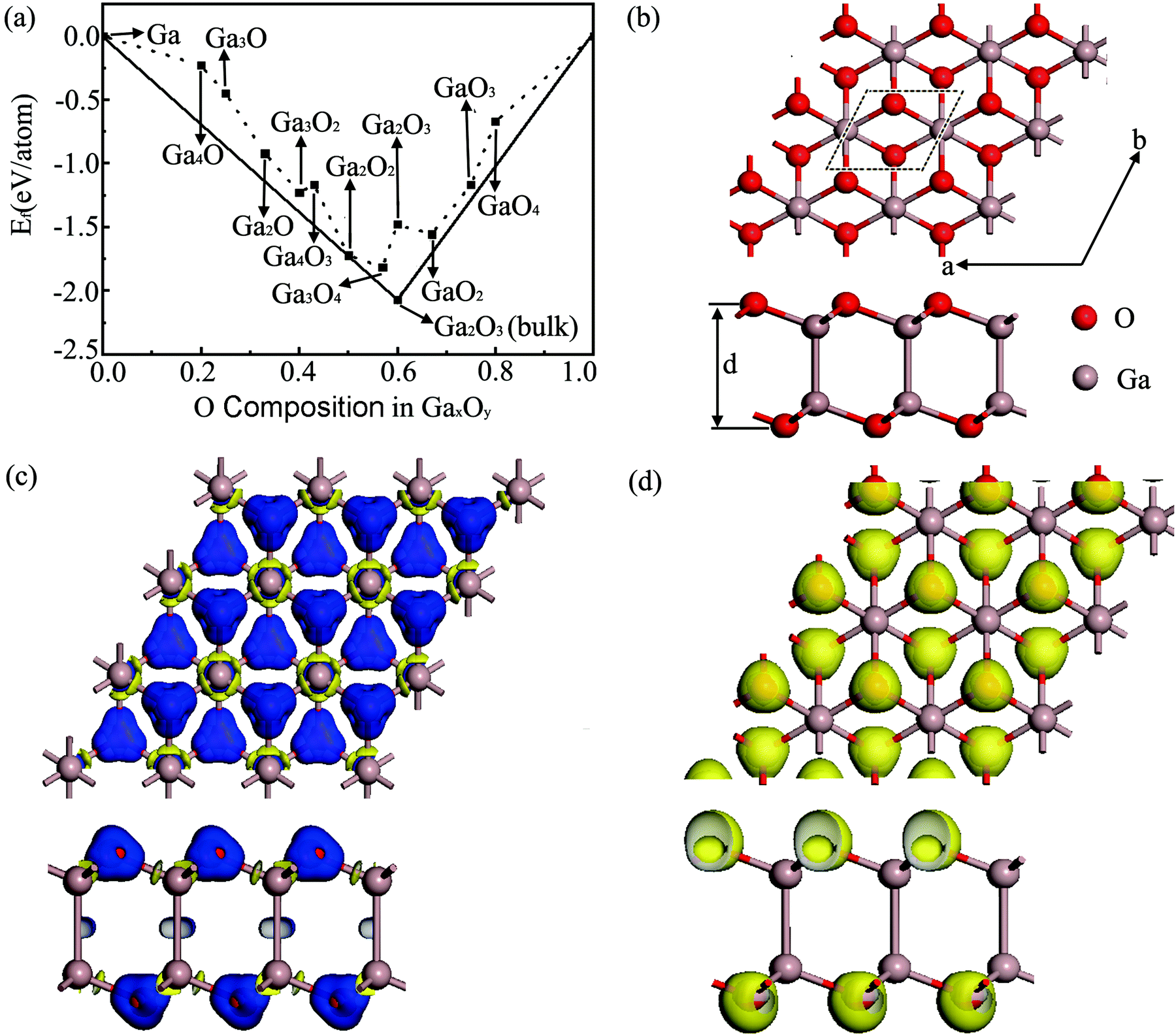 | ||
| Fig. 1 (a) Formation energy per atom as a function of the molar fraction of O atoms for different Ga–O phases. (b) Top and side views of the optimized 2D Ga2O2 sheet. The black dashed line shows the unit cell. (c) Charge density difference of Ga2O2 with an isovalue of ±0.1 e Å−3 (top and side views). (d) ELF map for the Ga2O2 sheet with an isosurface of 0.75 (top and side views). | ||
As shown in Fig. 1(b), one unit cell of this Ga2O2 sheet consists of two Ga and two O atoms inside, which is isostructural to the structure of the T-B2S2 monolayer28 but with slightly different structure parameters. The crystal structure of the Ga2O2 sheet possesses two stacked Ga–O layers with a bulking height d (the distance between the two external O atomic planes) of 4.065 Å. Its in-plane lattice constants are a = b = 3.062 Å. Each O atom is tri-coordinated with three adjacent Ga atoms, and each Ga atom bonds with three intra-layer O atoms and one Ga atom in the other layer. The average Ga–O bond distance is 1.926 Å, while that of the interlayer Ga–Ga bond is 2.501 Å.
The atomic charges estimated from Hirshfeld charge analysis show that the more electronegative O atoms get 0.32 e from the less electronegative Ga atoms on average. The deformation electron density (DED) images confirm the Hirshfeld analysis results. The DED is defined as the total electronic density of the Ga2O2 sheet with the contribution of isolated Ga and O atoms at their respective positions being subtracted. The result is visualized in Fig. 1(c), which indicates that the transferred electrons are shifted toward O atoms, showing ionic bond character. Yellow and blue refer to electron loss and accumulation regions, respectively. The calculated electron localization function (ELF)29,30 with an isosurface of 0.75 shown in Fig. 1(d) provides deeper insight into the chemical bonds of the predicted Ga2O2 sheet. A substantial concentration of electrons is tightly localized around O atoms and absent in the middle region between Ga and O atoms, which indicates distinct features of ionic bonding. Ga–Ga atoms interact in relatively weak covalent bonds in the Ga2O2 sheet. We also found that the length of the Ga–Ga bond in the H2Ga–GaH2 molecule31 is 2.464 Å, which is shorter than those in the Ga2O2 monolayer (2.501 Å). It means that the Ga–Ga bond in the H2Ga–GaH2 molecule is stronger than those in the Ga2O2 sheet. The electron transfer demonstrated by the DED and the bonding character indicated by the ELF partially contribute to the high structural stability of the Ga2O2 sheet.
To further clarify the energetic stability of the predicted new structure, we calculate the cohesive energy, Ec, of the Ga2O2 sheet and bulk Ga2O3. The calculated cohesive energies of them are 5.349 and 5.497 eV per atom, respectively. A rather favorable Ec indicates a stably connected network and its synthetic feasibility. Ec of the Ga2O2 sheet is slightly smaller than that of bulk Ga2O3, but it is higher than those of some experimentally synthesized 2D compounds, such as silicene (4.659 eV per atom)32 and germanene (4.051 eV per atom),33 and is just lower than that of borophene (5.582 eV per atom),34,35 computed at the same level of theory. The dynamical stability of the Ga2O2 sheet is confirmed by the phonon spectrum calculation. As shown in Fig. 2(a), the absence of appreciable imaginary vibrational modes in the entire Brillouin zone confirms the robustness of the interaction between Ga and O at 0 K and the Ga2O2 sheet can exist as a free-standing 2D structure. It is noteworthy that the maximum frequency of the Ga2O2 sheet is 603 cm−1 (18.1 THz), which is greater than those of AuGaS2 monolayers (∼450 cm−1),36 the Cu2S monolayer (∼390 cm−1),37 the GeP2 monolayer (∼500 cm−1),38 the InO monolayer (∼400 cm−1),39 and gold sulfide monolayers (∼400 cm−1),40 attesting robust chemical bonds in the sheet. On the other hand, to examine the thermal stability of the Ga2O2 sheet, AIMD simulations were carried out. The fluctuation of the total potential energy as a function of simulation time is plotted in Fig. 2(b). After heating at 300 and 1000 K for 10 ps, we can find that the original configuration of the Ga2O2 monolayer does not experience serious disruption and the total energy is fluctuant between −535 eV and −527 eV during the entire simulation. At a temperature of 1500 K, the Ga2O2 sheet is highly distorted within 10 ps of AIMD simulation (Fig. S1(a) in the ESI†). A temperature of 1000 K is high enough for many practical applications. These results reveal that the Ga2O2 sheet possesses good thermal and dynamical stability and is expected to be synthesized under certain experimental conditions.
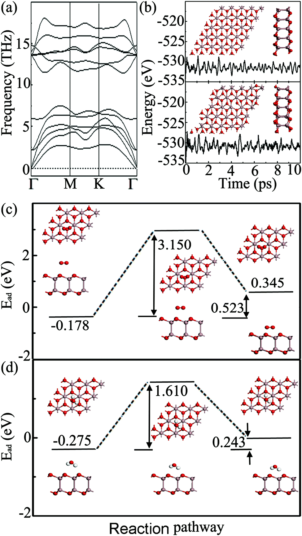 | ||
| Fig. 2 (a) Phonon dispersion of the Ga2O2 sheet. (b) Total energy fluctuation as a function of molecular dynamics simulation time and corresponding snapshots after equilibration for the Ga2O2 sheet at 300 K (top) and 1000 K (down). The reaction pathway and energy barrier for O2 (c) and H2O (d) molecules from physisorption to chemisorption on the surface of a Ga2O2 sheet. | ||
Note that phosphorene will experience rapid degradation after exfoliation because it can be easily oxidized by the O2 and H2O in the open-air environment, which restricts its applications.41,42 Therefore, examining the oxidation capability of the Ga2O2 sheet under ambient conditions becomes critical. Various O2/H2O adsorption geometries are compared by calculating their adsorption energies. It is found that the O2/H2O molecule tends to be adsorbed on the hollow site above the center of the Ga–O hexagon with three nearest-neighbor O atoms of Ga2O2. The small absolute adsorption energy of −0.178/−0.275 eV indicates a feature of physical adsorption, suggesting the oxidation resistance of the Ga2O2 sheet. To further support this conclusion, we calculated the energy barrier from physisorption to chemisorption of an O2/H2O molecule on the surface of the Ga2O2 sheet with the CI-NEB method. The activation energy barriers are 3.150/1.610 eV, much higher than that of phosphorene (∼0.7 eV),43 indicating that the Ga2O2 monolayer might be chemically stable in the air at low temperatures. As presented in Fig. 2(c) and (d), the product of the reaction has an energy 0.523/0.243 eV higher than that of the reactant, indicating that this reaction process is endothermic. Furthermore, we simulated dynamical oxidation processes at 300 K, by using AIMD simulations, with twelve O2/H2O molecules preadsorbed above and below a 5 × 5 × 1 Ga2O2 supercell. As shown in Fig. S1 (ESI†), after 5 ps of MD simulation with a time step of 1 fs, the Ga2O2 monolayer retains its initial configuration and O2/H2O molecules move away from the monolayer without dissociation. As a result, the Ga2O2 monolayer is expected to exhibit reasonable chemical inertness in ambient air and this unique stability might be attributed to the repulsion between O atoms of the Ga2O2 monolayer and O atoms in O2/H2O.
The mechanical stability is also indispensable for its applications in the real world. The linear elastic constants, Young's modulus, and Poisson's ratio of the Ga2O2 sheet are computed and listed in Table 1. The calculated elastic constants satisfy the stability criteria for 2D materials: C11 > |C12| and C66 > 0,44,45 implying that the proposed structure is mechanically stable. The in-plane Young's modulus Y and Poisson's ratio ν can be deduced from the elastic constants by Y = (C112 − C122)/C11 and ν = C12/C11, respectively. To evaluate the accuracy, the results of graphene are also presented at the same level of DFT. The calculated Y and ν values for graphene are in good agreement with previous theoretical studies.46,47 We found that the Y value of graphene (353.1 N m−1) is almost triple that of the Ga2O2 sheet (121.3 N m−1), while the ν value of the Ga2O2 sheet is about double that of graphene.
| C 11 | C 12 | C 66 | Y | ν | |
|---|---|---|---|---|---|
| Ga2O2 | 142.4 | 54.8 | 17.6 | 121.3 | 0.385 |
| Graphene | 366.0 | 68.6 | 136.3 | 353.1 | 0.187 |
The band structure of the Ga2O2 sheet at the PBE level is presented in Fig. 3(a). The Ga2O2 monolayer has an indirect gap (Eg) of 1.550 eV with the valence band maximum (VBM) located in the interval of K–Γ and the conduction band minimum (CBM) situated at the Γ point in the irreducible BZ. To get a more accurate band gap, we have also calculated the band structure and density of states (DOS) of the Ga2O2 monolayer by the hybrid HSE06 scheme. The results using HSE06 yield similar band shapes, but the Eg value increases to 2.752 eV (Fig. 3(a)). It is much smaller than that of bulk Ga2O3 (∼4.8 eV).1–6 The projected DOS (PDOS) suggests that the VBM of the Ga2O2 sheet is mainly dominated by the hybridization of Ga_4s orbitals and O_2p orbitals, while the contributions of Ga_4p states are negligible.
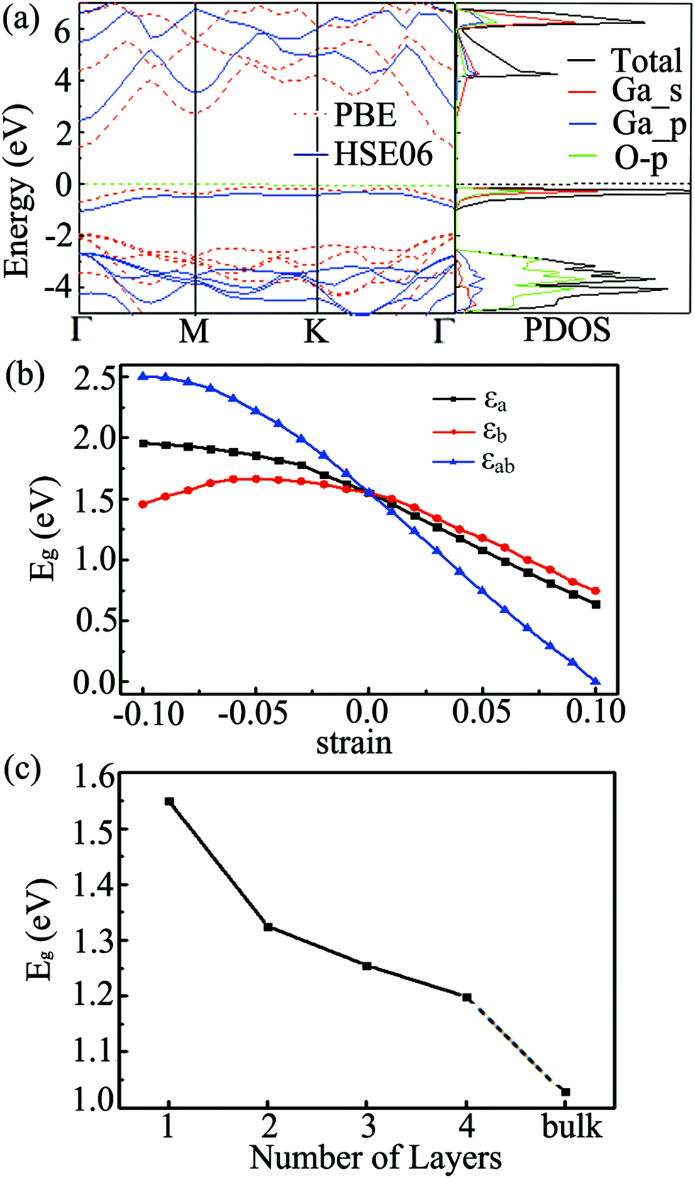 | ||
| Fig. 3 (a) Computed PBE (red dashed lines) and HSE06 (blue solid lines) band structure of the Ga2O2 sheet and its HSE06 PDOS. The Fermi level is set to zero. The band gap of the Ga2O2 sheet at the PBE level as a function of strain εa, εb and εab (b) and number of layers (c). | ||
As a 2D monolayer material, the electronic properties of the Ga2O2 sheet can be engineered by applying strain. We have investigated uniaxial and biaxial (tensile and compressive) strains and the simulated strains εa, εb and εab vary from −10% to 10%. We found that the Ga2O2 sheet shows no obstructive structural change under strain in the range of −10 to 10%. The evolution of the band structure with strain is demonstrated in Fig. S2 (ESI†). As seen in Fig. 3(b) and Fig. S2 (ESI†), the band gap increases with compressive strain and decreases with tensile strain for εa and εab in the Ga2O2 sheet. Eg increases for smaller compressive strain and starts to decrease at a strain of −6% for εb, which differs from the trend of monotonic decreasing from compression to tension as found for εa and εab. The decreasing tendencies are quasi-linear from −3% to 10% for the three strains. The bandgaps are more sensitive to biaxial strains than to uniaxial ones. The indirect-gap semiconducting nature of the Ga2O2 sheet is sustained independently of the directions of the applied strains except Eg declines to 0 at the PBE level under 10% biaxial tensile stress. These properties suggest that the band gap of the Ga2O2 sheet can be easily tuned by uniaxial and biaxial strains.
The electronic properties of 2D materials change with the layer numbers and the stacking patterns. Two possible high-symmetry stacking patterns of the Ga2O2 bilayer, namely AA and AB configurations, were considered (Fig. S3, ESI†). The optimized interlayer distance of AA stacking of the Ga2O2 bilayer (2.655 Å) is less than that of the AB bilayer (2.751 Å). The binding energy of the Ga2O2 AA bilayer (74 meV) is comparable to that of the AB bilayer (73 meV). As expected, the band gap of the Ga2O2 bilayer in the AA stacking configuration is reduced to 1.325 eV (Fig. 3(c) and Fig. S3, ESI†) compared to that of the monolayer (1.550 eV) from the PBE calculation. Increasing the stacking to tri- and four-layer (AA stacking), the corresponding band gaps are 1.255 and 1.199 eV (PBE level), respectively. The indirect-gap semiconducting feature in the AA stacking Ga2O2 bulk is kept but with a further reduced band gap of 1.028 eV. Therefore, the bandgap of Ga2O2 can also be tuned by increasing the number of layers, and shows a monotonic decreasing trend with increasing layers. The exfoliation energy of the Ga2O2 monolayer is 0.382 J m−2, which is smaller than that of the P3C monolayer (0.404 J m−2),12 δ-InP3 monolayer (0.827 J m−2),48 and Cd2C monolayer (∼0.48 J m−2).49 It holds great promise to fabricate this novel Ga2O2 monolayer in the laboratory by exfoliating Ga2O2 multilayer materials. For the convenience of experimental comparison in the future, we calculated scanning tunneling microscopy (STM) images of the Ga2O2 sheet (using the constant height model50 with a height of 1.0 Å and a negative bias of 0.2 V, Fig. S4(a), ESI†). The Raman spectrum was also simulated based on the phonon vibrational modes at the first BZ center, as shown in Fig. S4(b) (ESI†). The Raman active mode at 197 cm−1 for the Ga2O2 monolayer is slightly lower than the characteristic band centered at approximately 200 cm−1 of β-Ga2O3 thin films.51 The Raman feature would be useful for future experimental characterization of the Ga2O2 monolayer.
The performance of electronic and photoelectronic devices is strongly affected by the carrier transport properties of semiconducting materials. Here, the model of the Ga2O2 monolayer was rebuilt in an orthogonal supercell to estimate the carrier mobility along the x and y directions. The atomic structure of the supercell and the corresponding electronic band structure with the HSE06 hybrid functional are presented in Fig. S5 (ESI†). The obtained effective mass m*, elastic modulus C2D, deformation potential constant EDP, carrier mobility μ, and relaxation time τ for the Ga2O2 monolayer are summarized in Table 2. As listed in Table 2, the effective mass shows an obviously anisotropic feature, due to the different atomic arrangements along the x and y directions. The effective mass of a hole is approximately six times larger than that of an electron along the x direction, which can be understood by the quite flat valence band and more dispersive conduction band (Fig. S5, ESI†). The shifts of the band edges as a function of uniaxial strain show significant distinction for electrons and holes (Fig. 4(a)). To our surprise, the absolute values of the deformation potential constants in Ga2O2 are 0.38 eV (x direction) and 0.41 eV (y direction) for holes, which are an order of magnitude smaller than those of electrons (5.93 and 5.54 eV along the x and y directions, respectively). The calculated acoustic-phonon-limited hole mobilities in Ga2O2 at room temperature (T = 300 K) are 3027.94 and 4720.40 cm2 V−1 s−1 along the x and y directions, respectively. The electron mobilities are remarkably smaller than those of holes in both transport directions with values of 397.60 (x direction) and 407.09 cm2 V−1 s−1 (y direction). Electrons display less pronounced anisotropy than holes in mobility along the two directions. The large difference between the electron and hole mobilities is more ascribed to their different deformation potential constants rather than effective masses. The disparity in the electron and hole mobilities (e.g., 10 times larger for holes along the y direction) may be utilized for separating electrons and holes. These results can be explained by the real-space charge density distributions of the VBM and CBM in Fig. 4(b) and (c), respectively. Fig. 4(b) shows that VBM electron states are distributed more along the y direction than along the x direction, indicating that the lattice deformation in the x direction has less effect on the VBM positions. So, the carrier transport along the y direction is relatively easier than along the x direction. Meanwhile, for the CBM, the charges are almost symmetrically distributed (Fig. 4(c)), leading to the similar electron mobility along different directions. Interestingly, the hole mobilities of the Ga2O2 monolayer far surpass those of the recently reported SN2 monolayer (1160 cm2 V−1 s−1)46 and hydrogenated PtP2 monolayer (2260 cm2 V−1 s−1),52 and are comparable with those in the kagome-Sb monolayer (4570 cm2 V−1 s−1)53 at room temperature. Our predicted Ga2O2 monolayer has both a large band gap and high hole mobilities, novel features highly desirable for practical applications.
| Carrier type | Direction | m* | C 2D | E DP | μ | τ |
|---|---|---|---|---|---|---|
| e | x | 0.42 | 121.31 | 5.93 | 397.60 | 0.09 |
| y | 0.47 | 121.31 | 5.54 | 407.09 | 0.11 | |
| h | x | 2.49 | 121.31 | 0.38 | 3027.94 | 4.28 |
| y | 1.62 | 121.31 | 0.41 | 4720.40 | 4.34 |
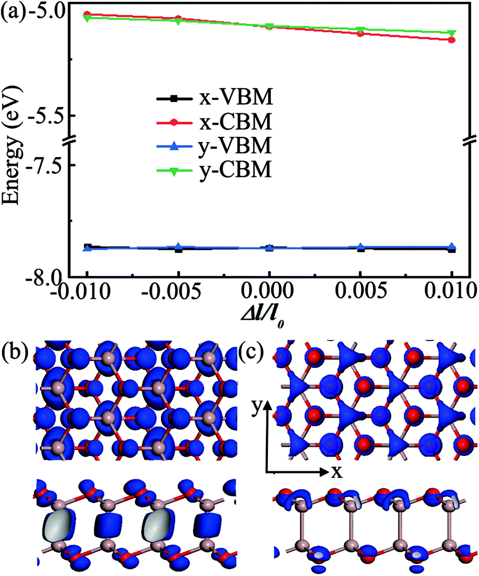 | ||
| Fig. 4 (a) Band edge position shifts of the VBM and CBM of the Ga2O2 monolayer with respect to the lattice distortion along the x and y directions. Charge densities for the VBM (b) and CBM (c) of the Ga2O2 monolayer (top and side views). The isosurface value is taken as 0.05 e Å−3. | ||
The Ga2O2 monolayer is an indirect and wide gap semiconductor and it is beneficial to restrain the recombination of photo-activated electron–hole pairs.46 Thus, the light-harvesting performance of the Ga2O2 monolayer and bilayer is explored by computing the absorption coefficients based on the HSE06 functional and the absorption spectra for electric field polarizations along the x, y and z directions are displayed in Fig. 5. Both of them show high absorption coefficients (>105 cm−1), which are comparable to those of perovskites used in solar cells.54,55 Moreover, their absorption coefficients along the x and y directions are nearly equal, as observed in hydrogenated PtP252 and PC6 monolayers,56 but different from those of 2D B4O,57 while the intrinsic anisotropy between the in-plane x/y direction and out-of-plane z direction absorption coefficients is also observed due to the 2D nature. The bilayer exhibits stronger absorption than the monolayer. The position of the first absorption peak is located at about 4.0 eV (310 nm) for the Ga2O2 monolayer, which is higher than those (240 and 255 nm) of the response peaks of β-Ga2O3 thin films.51 Hence, with sizable absorption coefficients in the ultraviolet range, the Ga2O2 monolayer and bilayer may be very promising materials for future optoelectronic devices.
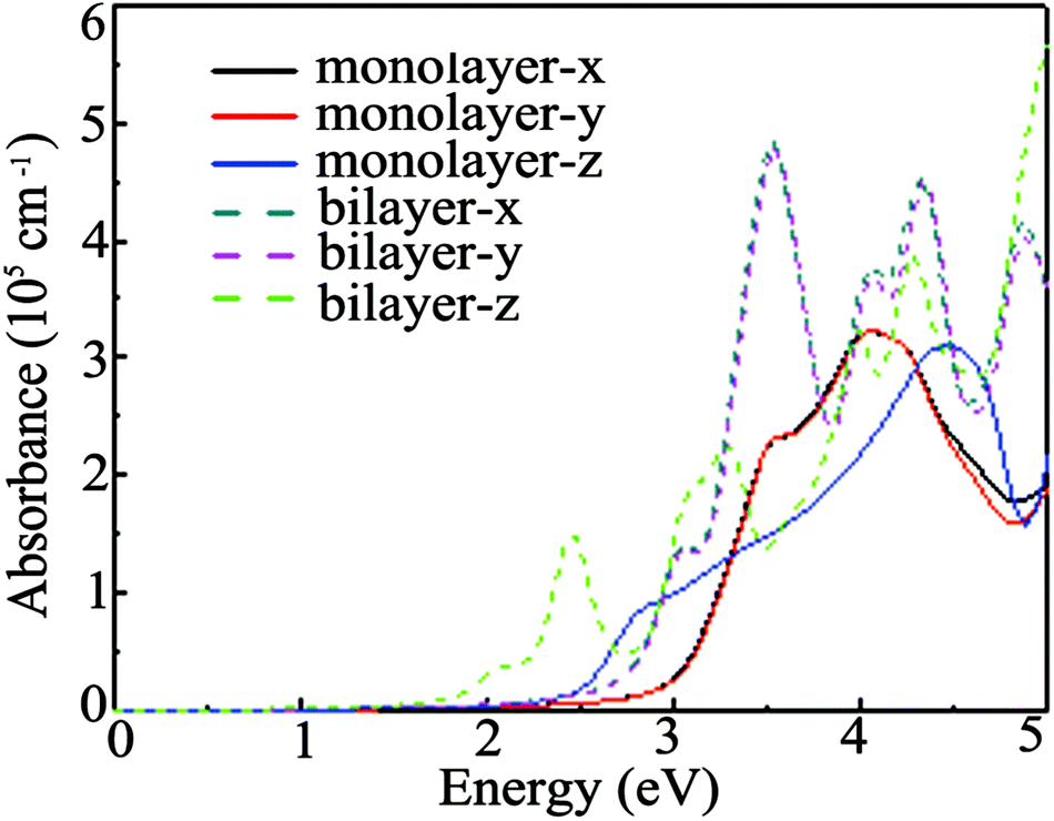 | ||
| Fig. 5 Calculated optical absorption spectra of the Ga2O2 monolayer and bilayer at the HSE06 level. | ||
Conclusions
In summary, we have identified a hitherto unknown 2D Ga2O2 monolayer material with desired electronic properties based on comprehensive first-principles swarm-intelligence structural search calculations. The Ga2O2 monolayer has excellent thermal and dynamical stabilities, providing a high possibility for its experimental viability or mechanical exfoliation from a multilayer. We have also verified that the Ga2O2 monolayer can withstand oxidation in air. The Ga2O2 monolayer has an indirect band gap of 2.752 eV on the basis of the HSE06 hybrid functional, and the band gap has a response to uniaxial and biaxial strains as well as the layer number. It possesses high room-temperature hole mobility up to 4720 cm2 V−1 s−1 and the large difference between the hole and electron mobility can be valuable for the efficient separation of holes and electrons. It exhibits notable optical properties in the ultraviolet wavelength region, with adsorption coefficients above 105 cm−1. All these data make the Ga2O2 monolayer a very promising material for 2D electronic and photoelectronic applications.Conflicts of interest
There are no conflicts to declare.Acknowledgements
We gratefully acknowledge the financial support from the National Natural Science Foundation of China (No. 11704344 and 11404253), the Aeronautical Science Foundation of China (No. 2017ZC55006 and 2019ZF055002), key scientific and technological project of Henan Province (No. 202102210052), and the Key Research Project of Colleges and Universities in Henan Province (No. 18A140033 and 19A140020). We thank Pengyue Gao and Bo Gao for helpful suggestions.References
- J. J. Xu, W. Zheng and F. Huang, J. Mater. Chem. C, 2019, 7, 8753–8770 RSC.
- X. Y. Zhang, Z. Z. Zhang, J. Liang, Y. C. Tong, Y. Wang and X. X. Wang, J. Mater. Chem. A, 2017, 5, 9702–9708 RSC.
- M. Higashiwaki and G. H. Jessen, Appl. Phys. Lett., 2018, 112, 060401 CrossRef.
- Y. W. Zhang, A. Neal, Z. B. Xia, C. Joishi, J. M. Johnson, Y. H. Zheng, S. Bajaj, M. Brenner, D. Dorsey, K. Chabak, G. Jessen, J. Hwang, S. Mou, J. P. Heremans and S. Rajan, Appl. Phys. Lett., 2018, 112, 173502 CrossRef.
- S. Y. Lee and H. C. Kang, Jpn. J. Appl. Phys., 2018, 57, 01AE02 CrossRef.
- A. I. Pechnikov, S. I. Stepanov, A. V. Chikiryaka, M. P. Scheglov, M. A. Odnobludov and V. I. Nikolaev, Semiconductors, 2019, 53, 780–783 CrossRef CAS.
- P. Miró, M. Audiffred and T. Heine, Chem. Soc. Rev., 2014, 43, 6537–6554 RSC.
- K. S. Novoselov, A. K. Geim, S. V. Morozov, D. Jiang, Y. Zhang, S. V. Dubonos, I. V. Grigorieva and A. A. Firsov, Science, 2004, 306, 666–669 CrossRef CAS PubMed.
- K. F. Mak, C. Lee, J. Hone, J. Shan and T. F. Heinz, Phys. Rev. Lett., 2010, 105, 136805 CrossRef PubMed.
- L. K. Li, Y. J. Yu, G. J. Ye, Q. Q. Ge, X. D. Ou, H. Wu, D. L. Feng, X. H. Chen and Y. B. Zhang, Nat. Nanotechnol., 2014, 9, 372–377 CrossRef CAS PubMed.
- W. Feng, X. N. Wang, J. Zhang, L. F. Wang, W. Zheng, P. A. Hu, W. W. Cao and B. Yang, J. Mater. Chem. C, 2014, 2, 3254–3259 RSC.
- J. Kim, S. Oh, M. A. Mastro and J. Kim, Phys. Chem. Chem. Phys., 2016, 18, 15760–15764 RSC.
- Y. Q. Wang, L. X. Song, Y. Teng, F. Wang, W. P. Wang, M. M. Ruan, Z. Yang and Z. Y. Xu, J. Mater. Chem. C, 2019, 7, 1477–1483 RSC.
- A. Zavabeti, J. Z. Ou, B. J. Carey, N. Syed, R. Orrell-Trigg, E. L. H. Mayes, C. L. Xu, O. Kavehei, A. P. O’Mullane, R. B. Kaner, K. Kalantar-zadeh and T. Daeneke, Science, 2017, 358, 332–335 CrossRef CAS PubMed.
- H. Peelaers and C. G. V. D. Walle, Phys. Rev. B, 2017, 96, 081409 CrossRef.
- Y. C. Wang, J. Lv, L. Zhu and Y. M. Ma, Phys. Rev. B: Condens. Matter Mater. Phys., 2010, 82, 094116 CrossRef.
- Y. C. Wang, M. S. Miao, J. Lv, L. Zhu, K. T. Yin, H. Y. Liu and Y. M. Ma, J. Chem. Phys., 2012, 137, 224108 CrossRef.
- J. P. Perdew, K. Burke and M. Ernzerhof, Phys. Rev. Lett., 1996, 77, 3865 CrossRef CAS PubMed.
- G. Kresse and J. Hafner, Phys. Rev. B: Condens. Matter Mater. Phys., 1993, 47, 558 CrossRef CAS PubMed.
- G. Kresse and J. Furthmüller, Phys. Rev. B: Condens. Matter Mater. Phys., 1996, 54, 11169 CrossRef CAS PubMed.
- S. Grimme, J. Antony, S. Ehrlich and H. Krieg, J. Chem. Phys., 2010, 132, 154104 CrossRef PubMed.
- J. Heyd, G. E. Scuseria and M. Ernzerhof, J. Chem. Phys., 2003, 118, 8207–8215 CrossRef CAS.
- X. Gonze and C. Lee, Phys. Rev. B: Condens. Matter Mater. Phys., 1997, 55, 10355–10368 CrossRef CAS.
- A. Togo, F. Oba and I. Tanaka, Phys. Rev. B: Condens. Matter Mater. Phys., 2008, 78, 134106 CrossRef.
- G. J. Martyna, M. L. Klein and M. Tuckerman, J. Chem. Phys., 1992, 97, 2635–2643 CrossRef.
- G. Henkelman, B. P. Uberuaga and H. Jonsson, J. Chem. Phys., 2000, 113, 9901–9904 CrossRef CAS.
- G. Henkelman and H. Jonsson, J. Chem. Phys., 2000, 113, 9978–9985 CrossRef CAS.
- C. Tang, F. X. Ma, C. M. Zhang, Y. L. Jiao, S. K. Matta, K. Ostrikov and A. J. Du, J. Mater. Chem. C, 2019, 7, 1651–1658 RSC.
- A. D. Becke and K. E. Edgecombe, J. Chem. Phys., 1990, 92, 5397–5403 CrossRef CAS.
- B. Silvi and A. Savin, Nature, 1994, 371, 683–686 CrossRef CAS.
- X. F. Wang and L. Andrews, J. Phys. Chem. A, 2003, 107, 11371–11379 CrossRef CAS.
- S. Cahangirov, M. Topsakal, E. Aktürk, H. Şahin and S. Ciraci, Phys. Rev. Lett., 2009, 102, 236804 CrossRef CAS PubMed.
- A. Fleurence, R. Friedlein, T. Ozaki, H. Kawai, Y. Wang and Y. Yamada-Takamura, Phys. Rev. Lett., 2012, 108, 245501 CrossRef.
- B. J. Feng, J. Zhang, Q. Zhong, W. B. Li, S. Li, H. Li, P. Cheng, S. Meng, L. Chen and K. H. Wu, Nat. Chem., 2016, 8, 563 CrossRef CAS.
- A. J. Mannix, X. F. Zhou, B. Kiraly, J. D. Wood, D. Alducin, B. D. Myers, X. L. Liu, B. L. Fisher, U. Santiago, J. R. Guest, M. J. Yacaman, A. Ponce, A. R. Oganov, M. C. Hersam and N. P. Guisinger, Science, 2015, 350, 1513–1516 CrossRef CAS PubMed.
- Q. Wu, W. W. Xu, L. Ma, J. L. Wang and X. C. Zeng, ACS Appl. Mater. Interfaces, 2018, 10, 16739–16746 CrossRef CAS PubMed.
- Y. Guo, Q. S. Wu, Y. H. Li, N. Lu, K. K. Mao, Y. Z. Bai, J. J. Zhao, J. L. Wang and X. C. Zeng, Nanoscale Horiz., 2018, 4, 223–230 RSC.
- F. Shojaei, J. R. Hahn and H. S. Kang, J. Mater. Chem. A, 2017, 5, 22146–22155 RSC.
- Y. Guo, L. Ma, K. K. Mao, M. G. Ju, Y. Z. Bai, J. J. Zhao and X. C. Zeng, Nanoscale Horiz., 2019, 4, 592–600 RSC.
- Q. S. Wu, W. W. Xu, D. D. Lin, J. L. Wang and X. C. Zeng, J. Phys. Chem. Lett., 2019, 10, 3773–3778 CrossRef CAS PubMed.
- A. Ziletti, A. Carvalho, D. K. Campbell, D. F. Coker and A. H. C. Neto, Phys. Rev. Lett., 2015, 114, 046801 CrossRef CAS PubMed.
- A. H. Woomer, T. W. Farnsworth, J. Hu, R. A. Wells, C. L. Donley and S. C. Warren, ACS Nano, 2015, 9, 8869–8884 CrossRef CAS PubMed.
- Y. Guo, S. Zhou, Y. Z. Bai and J. J. Zhao, ACS Appl. Mater. Interfaces, 2017, 9, 12013–12020 CrossRef CAS PubMed.
- F. Mouhat and F. X. Coudert, Phys. Rev. B: Condens. Matter Mater. Phys., 2014, 90, 224104 CrossRef.
- C. Z. Zhang and Q. Sun, J. Phys. Chem. Lett., 2016, 7, 2664–2670 CrossRef CAS.
- F. Y. Li, X. D. Lv, J. X. Gu, K. X. Tu, J. Gong, P. Jin and Z. F. Chen, Nanoscale, 2019, 12, 85–92 RSC.
- G. X. Wang, R. Pandey and S. P. Karna, Nanoscale, 2016, 8, 8819–8825 RSC.
- W. C. Yi, X. Chen, Z. X. Wang, Y. C. Ding, B. C. Yang and X. B. Liu, J. Mater. Chem. C, 2019, 7, 7352–7359 RSC.
- L. B. Meng, S. Ni, Y. J. Zhang, B. Li, X. W. Zhou and W. D. Wu, J. Mater. Chem. C, 2018, 6, 9175–9180 RSC.
- J. Tersoff and D. R. Hamann, Phys. Rev. B: Condens. Matter Mater. Phys., 1985, 31, 805–813 CrossRef CAS PubMed.
- X. H. Chen, S. Han, Y. M. Lu, P. J. Cao, J. W. Liu, Y. X. Zeng, F. Jia, W. Y. Xu, X. K. Liu and D. L. Zhu, J. Alloys Compd., 2018, 747, 869–878 CrossRef CAS.
- C. Y. Pu, J. H. Yu, R. M. Yu, X. Tang and D. W. Zhou, J. Mater. Chem. C, 2019, 7, 12231–12239 RSC.
- J. J. Zhu, C. He, Y. H. Zhao and B. T. Fu, J. Mater. Chem. C, 2020, 8, 2732–2740 RSC.
- N. J. Jeon, J. H. Noh, Y. C. Kim, W. S. Yang, S. Ryu and S. I. Seok, Nat. Mater., 2014, 13, 897–903 CrossRef CAS PubMed.
- M. Shirayama, H. Kadowaki, T. Miyadera, T. Sugita, M. Tamakoshi, M. Kato, T. Fujiseki, D. Murata, S. Hara and T. N. Murakami, Phys. Rev. Appl., 2016, 5, 014012 CrossRef.
- T. Yu, Z. Y. Zhao, Y. H. Sun, A. Bergara, J. Y. Lin, S. T. Zhang, H. Y. Xu, L. J. Zhang, G. C. Yang and Y. C. Liu, J. Am. Chem. Soc., 2019, 141, 1599–1605 CrossRef CAS.
- R. Q. Zhang, Z. Y. Li and J. L. Yang, J. Phys. Chem. Lett., 2017, 8, 4347–4353 CrossRef CAS PubMed.
Footnote |
| † Electronic supplementary information (ESI) available: Computational details, AIMD simulations, band structures, STM image, Raman spectrum, and atomic structure. See DOI: 10.1039/d0cp05171c |
| This journal is © the Owner Societies 2021 |