
 Open Access Article
 This Open Access Article is licensed under a
 Creative Commons Attribution 3.0 Unported Licence
Enhanced ion transport in Li2O and Li2S films†
Simon
Lorger
 ,
Kai
Narita
,
Robert
Usiskin
* and
Joachim
Maier
,
Kai
Narita
,
Robert
Usiskin
* and
Joachim
Maier
Max Planck Institute for Solid State Research, Heisenbergstraße 1, Stuttgart 70569, Germany. E-mail: r.usiskin@fkf.mpg.de
First published on 8th June 2021
Abstract
Films of Li2O and Li2S grown by sputter deposition exhibit Li+ conductivity values at room temperature which are enhanced by 3–4 orders of magnitude relative to bulk samples. Possible mechanisms are discussed. The results may help explain the ion transport pathway through passivation layers containing these chalcogenides in batteries.
Lithium oxide (Li2O) and lithium sulfide (Li2S) are frequently encountered in batteries. They typically form as part of a solid–electrolyte interphase (SEI) passivation layer when a low-voltage anode reduces an electrolyte that contains the elements oxygen or sulfur.1–3 They are also an important reaction product in conversion electrodes based on oxides,4 oxygen,5 nitrates,6 sulfides,4 sulfur,7 and so on. The solid-state ion transport rates within the Li2O and Li2S can limit battery performance, yet the rates are not well-understood, partly because many phases are involved. To deconvolute the contributions and identify the rate-limiting mechanisms, it is valuable to study the individual materials in isolation.
The defect chemistry in bulk samples of Li2O and Li2S was characterized previously.8,9 Both compounds take the antifluorite structure and are well described by a defect chemical model based on Frenkel disorder. The Li+ conductivity can vary by orders of magnitude depending on doping, but the ionic defect mobilities are low, so even under favorable doping conditions, equilibrated bulk samples show an ionic conductivity at 25 °C below 10−10 S cm−1. This limit is 1–3 orders of magnitude lower than the ionic conductivity estimated for typical SEI layers containing Li2O or Li2S,1,2,10 as mentioned previously8,9 and discussed in more detail below. The disparity suggests that ion transport in SEI layers cannot be explained by simple models that consider only point defects in bulk-like Li2O and Li2S. However, higher-dimensional defects such as grain boundaries, dislocations, interfaces, and amorphous content sometimes provide faster transport paths, and such defects are often present in films. These points motivate a study of Li2O and Li2S films.
Such films have been systematically investigated only a few times previously. For Li2O, Kozen et al. prepared dense films using atomic layer deposition (ALD),11 and Wulfsberg et al. used electron microscopy to study lithium metal oxidation,12 but neither work discussed transport rates. Guo et al. grew Li2O films on Li metal by exposure to oxygen gas and measured a through-plane conductivity of 2 × 10⁻⁹ S cm−1 at 25 °C.10 For Li2S, Meng et al. grew XRD-amorphous films by ALD and demonstrated stable battery cycling performance.13 Klein et al. prepared Li2S films by RF sputtering14 and estimated the ionic conductivity after annealing at 600 °C to be 10−11 S cm−1 at 25 °C.15 It is also worth mentioning two studies that reached different conclusions about the impact of grain size. For Li2O, Indris et al. reported a negligible impact on ionic conductivity from reducing the grain size by ball milling.16 For Li2S, Lin et al. observed higher conductivity values from nanocrystalline material than from microcrystalline material,17 but all the values were anomalously low compared to other works on Li2S (cf. Fig. S3 in ref. 9). In a previous work, we explored how changing the deposition parameters affects the morphology of Li2O and Li2S films grown by sputter deposition or thermal evaporation.18 Here we discuss the behavior of sputter-deposited films grown with a dense nanocrystalline morphology. In particular, we focus on in-plane transport measurements, which are a standard method for probing interfacial effects in films19–21 while avoiding problems with short circuiting that can arise in a through-plane geometry.22 Experimental details are given in the ESI.†
Fig. 1 shows representative data from the structural characterization of the films. X-ray diffraction (XRD) patterns show only reflections corresponding to polycrystalline Li2O or Li2S with a preferred (111) out-of-plane orientation. Raman spectra show only peaks corresponding to Li2O, Li2S, and the Al2O3 substrate. The polysulfide species discussed in ref. 14 is not observed here, nor is LiOH. In cross-section images, the films appear dense with a fairly uniform thickness.
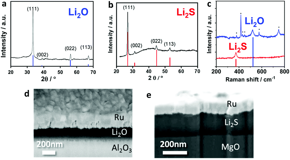 | ||
| Fig. 1 Typical structural characterization of films grown by sputter deposition. (a and b) X-ray diffraction patterns measured from Li2O grown on Al2O3 and Li2S grown on MgO. (c) Raman spectra. Asterisks denote Al2O3 peaks.23 (d and e) Focused ion beam–scanning electron microscopy cross-section images, which include the Ru electrodes used for transport measurements. Films were grown from elemental sources in (b–e) and a Li2O source in (a). In (a–c), the peak positions reported for bulk samples are indicated by vertical lines.24–27 | ||
A schematic of the in-plane configuration used for transport measurements is shown in Fig. S1a (ESI†), and example impedance spectra are shown in Fig. S1b (ESI†). The presence of a low-frequency arc is consistent with blocking of mobile Li+ at the metal electrodes. The capacitance of the main semicircle corresponds to stray capacitance from the substrate.28–30 The macroscopic conductivity σm extracted from the resistance of the main semicircle is displayed in Fig. 2. As grown, the films of each material show an in-plane conductivity which is higher than that of lightly-doped bulk samples by 3–4 orders of magnitude near room temperature. The values are stable over repeated thermal cycles below the growth temperature, which was 150 °C for Li2O and 290 °C for Li2S. The activation energy (determined from the slope of σmT) is 0.5–0.6 eV for the Li2O films and 0.6 eV for the Li2S films. For Li2O, the as-grown conductivity shows some scatter; the data selected for Fig. 2 are representative of the extent of this scatter. A DC measurement performed on a Li2O film using Li+-selective electrodes shows a steady current over time (Fig. S2, ESI†), which provides further evidence that the mobile species is Li+ ions.
 | ||
| Fig. 2 In-plane macroscopic conductivity of films deposited on single crystal substrates using elemental targets: (a) Li2O films on Al2O3(0001), and (b) Li2S films on MgO(100). Measurements were acquired both as grown and after annealing at 340 °C. Solid lines are linear fits. Dotted curves correspond to bulk samples of (a) 0.1% LiF-doped Li2O8 and (b) 0.1% LiCl-doped Li2S.9 | ||
The behavior changes markedly upon annealing at higher temperature. After annealing at 340 °C, the films show reduced conductivity values which remain higher than those of 0.1%-doped bulk samples by 1–2 orders of magnitude. The values are stable over repeated thermal cycles from 25–340 °C, and the Li2O data show less scatter. The activation energy is about 0.85 eV for Li2O and 0.74 eV for Li2S. XRD patterns acquired after impedance measurements still show only Li2O or Li2S reflections, which rules out significant LiOH formation. Above 340 °C the transport behavior is difficult to assess, because the metal electrodes tend to coarsen and lose adhesion.
To gain further insight, the normalized conductance σmL after annealing is plotted in Fig. 3 as a function of film thickness. This representation is useful because --- assuming the body of the film has uniform properties --- the intercept obtained by extrapolating to zero thickness corresponds to the excess interfacial contribution.31 At various temperatures the intercept is indistinguishable from zero, indicating that the conductance after annealing arises from the body of the film, not the interfaces with the substrate or gas phase. This analytical approach could not be used for the as-grown Li2O data due to scatter, nor for the Li2S films due to a more limited dataset. However, further investigations of Li2O show that the conductivity results are largely unaffected when the single crystal substrate is switched from Al2O3(0001) to MgO(100), or MgF2(001), or LiF(111) (Fig. S3, ESI†). These data are strong evidence against a substrate-specific mechanism such as a space charge effect at the film-substrate interface, both before and after annealing. Also, essentially the same transport behavior (and morphology18) are observed in films grown from a ceramic Li2O target instead of elemental Li and O2 sources (Fig. S3, ESI†).
 | ||
| Fig. 3 Thickness dependence of the normalized conductance σmL after annealing at 340 °C. Films were grown using an elemental Li sputter target. Lines are linear fits. | ||
The transition during annealing is explored in Fig. S4 (ESI†). A useful clue emerges here, in that a mild anneal causes the conductivity to increase before decreasing. In particular, the conductivity of the Li2O films increases by about a factor of 4 during a mild anneal at 165 °C. The increase persists if the anneal is halted and the temperature lowered. The effect is smaller in Li2S films, but it still appears. Annealing also leads to grain growth. As grown, the grain size in the Li2O films is estimated to be 20–50 nm by SEM (Fig. S5, ESI†) and 20 nm by XRD; after annealing at 340 °C, the grain size increases to 50–200 nm by SEM and 60 nm by XRD. Similar findings are seen by SEM for the Li2S films. More details and representative data are given in ref. 18.
The dominant transport mechanism in the films is unclear. Measurements by XRD, Raman, and SEM show no evidence of an impurity phase. In particular, XRD confirmed the absence of LiOH in multiple films, both before and after impedance measurements. Since the ionic conductivity of bulk LiOH is comparable to that of bulk Li2O and Li2S, even if trace LiOH were present, it would not be expected to increase the conductivity.32 The measured conductivities are also too high to be explained by simple doping of bulk-like Li2O and Li2S. The concentration of mobile vacancies does not scale linearly with doping amount at these temperatures due to association effects, so to achieve in bulk samples the conductivity exhibited by the annealed films, dopant concentrations well in excess of 10 mol% (Li2O) and 1 mol% (Li2S) would be required.8,9 To explain the conductivity of the as-grown films, the required concentrations would be even higher. Such high doping levels are implausible, and they were not detected in TOF-SIMS measurements on a Li2O film, as described in the ESI.† Also, disassociation of defect pairs in doped bulk Li2O and Li2S leads to a reversible change in activation energy starting around 130–180 °C (e.g., the dotted curves in Fig. 2 start to bend). This behavior is absent in the annealed films. It is also quite unlikely that the enhanced conductivity is due to high lithium activity, for a few reasons. One, a high lithium activity is not expected, since the films were grown under excess oxygen or sulfur conditions. Two, the ionic defect concentrations in Li2O and Li2S are expected from fundamental defect chemistry to be essentially constant over a wide range of lithium activity, due to the predominant ionic disorder. See Fig. 4–8 in ref. 33 for more detail. Three, a high lithium activity would decrease the mobile Li+ vacancy concentration and the associated conductivity. It would also increase the concentration of interstitial Li+ ions, but they show a mobility at room temperature which is far too low to account for the observed conduction.8,9 In short, the film conductivities are inconsistent with bulk-like transport in Li2O and Li2S considering only point defects.
Experiments in other material systems offer clues about possible enhancement mechanisms. Consider fluorite CaF2, which exhibits the same crystal structure as antifluorite Li2O and Li2S. In a striking similarity to the present work, evaporated films of CaF2 show a F− conductivity that is enhanced by several orders of magnitude relative to lightly-doped bulk CaF2, and annealing the films at 340 °C yields a decreased enhancement and an increased activation energy.30,34 Another similarity is that for both CaF2 and Li2S films, increasing the growth temperature to 500–600 °C seems to eliminate the enhancement.18,21 These parallels are strong circumstantial evidence for a similar mechanism. In CaF2, grain boundaries35–37 and dislocations34 have been suggested to provide percolating fast pathways for F− transport. By analogy, one can hypothesize that grain boundaries and/or dislocations provide fast paths for Li+ transport in Li2O and Li2S, either along the defect cores or in the adjacent space charge zones and strain fields. Consistent with this hypothesis, the Li2O and Li2S films exhibit a substantially reduced density of grain boundaries after a 340 °C anneal. The change in activation energy upon annealing could, in principle, be due to a transition from dislocation-driven to grain-boundary-driven conduction and/or a space charge effect with a changing segregation energy. LiI films were also suggested to exhibit fast Li+ transport along dislocations that anneal out,38,39 and strong evidence of fast ion conduction along dislocations is available for TiO2.40,41 Fast transport along grain boundaries has been observed in several materials.42 Yet, this behavior is not universal, e.g., nanocrystalline LiF films grown on Al2O3 (using the same sputter deposition system as in this work) show a depressed conductivity and disordered structure near the LiF–Al2O3 interface.43
Alternatively, we cannot entirely rule out the presence of amorphous material. In CaF2 films grown on Al2O3, a few nm-thick amorphous layer was clearly observed at the CaF2–Al2O3 interface by high-resolution transmission electron microscopy (HRTEM); yet, the layer was absent for growth on MgO, and its absence did not appear to substantially affect the conductivity.30 HRTEM measurements of Li2O and Li2S films should be possible in future work using suitable transfer tools. The fact that the conductivity initially increases during annealing (Fig. S4, ESI†) excludes a simple mechanism based on a fast-conducting amorphous phase that crystallizes. However, fast ion transport at amorphous–crystalline interfaces is possible, and the density of those interfaces can initially increase during crystallization, as suggested in the LiF–SiO2,29 Agl–Ag2O–V2O5,44 and LiAlSiO445 systems. In all the mechanisms discussed in the last two paragraphs, the higher-dimensional defects percolate along the film, and the local conductivity varies spatially, with regions in proximity to the relevant defects showing a higher conductivity than the measured macroscopic value.
Let us compare the conductivities in this work with those reported for multiphase SEI layers and single-phase samples of common SEI components. For multiphase SEI layers from liquid carbonate electrolytes, Peled gave a typical resistance of 10–1000 Ω cm2 at 25 °C, which corresponds to 10−9–10−7 S cm−1 if a thickness of 10 nm is assumed.1 Guo et al. measured 5 × 10⁻¹⁰ S cm−1.10 For SEI layers from solid sulfide electrolytes, Wenzel et al. observed 10–5000 Ω cm2, or 2 × 10⁻¹⁰–10−7 S cm−1 assuming a 10 nm thickness. A similar range of values was observed by Sakuma et al.46 Despite uncertainty about the precise SEI thickness, these data suggest that typical SEI layers containing Li2O or Li2S show an overall ionic conductivity on the order of 10−10–10−7 S cm−1 at 25 °C. Fig. 4 compares this range to the ionic conductivity values at 25 °C measured by impedance spectroscopy from single-phase samples of common SEI constituents. Interestingly, none of the data from the individual bulk materials are consistent with the range of conductivities estimated for the multiphase SEI layers. On the other hand, the films in this work show macroscopic conductivities at 25 °C of 10−10–10−7 S cm−1 (Li2O) and 10−10–3 × 10⁻⁸ S cm−1 (Li2S), depending on annealing, which do agree with the SEI range. This crude comparison considers only the macroscopic ionic conductivities, and it deserves refinement in future work. Nevertheless, it suggests that higher-dimensional defects and interfaces associated with Li2O and Li2S may explain the Li+ transport mechanism in various SEI layers.
 | ||
| Fig. 4 Ionic conductivity at 25 °C of typical materials in SEI passivation layers, as measured from single-phase bulk or film samples by impedance spectroscopy in this work (green) or in the literature (gray). In many works a range of values has been measured, e.g., depending on doping. An asterisk indicates the values were estimated by extrapolation from data acquired at 100–300 °C and higher. For LiOH an upper bound is shown. Multiphase SEI layers containing Li2O or Li2S typically exhibit an ionic conductivity in the range shown (purple). See Tables S1 and S2 (ESI†) for references. LEMC is lithium ethylene monocarbonate. Adapted with permission from ref. 47. | ||
We are thankful for support from Dieter Fischer (XRD, Raman), Florian Kaiser (mechanical design), Bernhard Fenk (FIB-SEM), and Tolga Acatürk (SIMS). K. N. gratefully acknowledges financial support from the Masason Foundation.
Open Access funding provided by the Max Planck Society.
Conflicts of interest
There are no conflicts to declare.Notes and references
- E. Peled and S. Menkin, J. Electrochem. Soc., 2017, 164(7), A1703–A1719 CrossRef CAS.
- S. Wenzel, S. J. Sedlmaier, C. Dietrich, W. G. Zeier and J. Janek, Solid State Ionics, 2018, 318, 102–112 CrossRef CAS.
- W. Huang, P. M. Attia, H. Wang, S. E. Renfrew, N. Jin, S. Das, Z. Zhang, D. T. Boyle, Y. Li, M. Z. Bazant, B. D. McCloskey, W. C. Chueh and Y. Cui, Nano Lett., 2019, 19(8), 5140–5148 CrossRef CAS PubMed.
- J. Cabana, L. Monconduit, D. Larcher and M. R. Palacín, Adv. Mater., 2010, 22(35), E170–E192 CrossRef CAS PubMed.
- C. Xia, C. Y. Kwok and L. F. Nazar, Science, 2018, 361(6404), 777–781 CrossRef CAS PubMed.
- V. Giordani, D. Tozier, J. Uddin, H. J. Tan, B. M. Gallant, B. D. McCloskey, J. R. Greer, G. V. Chase and D. Addison, Nat. Chem., 2019, 11(12), 1133–1138 CrossRef CAS PubMed.
- P. G. Bruce, S. A. Freunberger, L. J. Hardwick and J. M. Tarascon, Nat. Mater., 2012, 11(1), 19–29 CrossRef CAS PubMed.
- S. Lorger, R. Usiskin and J. Maier, J. Electrochem. Soc., 2019, 166(10), A2215–A2220 CrossRef CAS.
- S. Lorger, R. Usiskin and J. Maier, Adv. Funct. Mater., 2019, 29, 1807688 CrossRef.
- R. Guo and B. M. Gallant, Chem. Mater., 2020, 32(13), 5525–5533 CrossRef CAS.
- A. C. Kozen, A. J. Pearse, C. F. Lin, M. A. Schroeder, M. Noked, S. B. Lee and G. W. Rubloff, J. Phys. Chem. C, 2014, 118(48), 27749–27753 CrossRef CAS.
- S. M. Wulfsberg, B. E. Koel and S. L. Bernasek, Surf. Sci., 2016, 651, 120–127 CrossRef CAS.
- X. B. Meng, D. J. Comstock, T. T. Fister and J. W. Elam, ACS Nano, 2014, 8(10), 10963–10972 CrossRef CAS PubMed.
- M. J. Klein, G. M. Veith and A. Manthiram, J. Am. Chem. Soc., 2017, 139(31), 10669–10676 CrossRef CAS PubMed.
- M. J. Klein, G. M. Veith and A. Manthiram, J. Am. Chem. Soc., 2017, 139(27), 9229–9237 CrossRef CAS PubMed.
- S. Indris, P. Heitjans, H. E. Roman and A. Bunde, Phys. Rev. Lett., 2000, 84(13), 2889–2892 CrossRef CAS PubMed.
- Z. Lin, Z. C. Liu, N. J. Dudney and C. D. Liang, ACS Nano, 2013, 7(3), 2829–2833 CrossRef CAS PubMed.
- S. Lorger, D. Fischer, R. Usiskin and J. Maier, J. Vac. Sci. Technol., A, 2019, 37(6), 11 CrossRef.
- C. L. Li and J. Maier, Solid State Ionics, 2012, 225, 408–411 CrossRef CAS.
- D. Pergolesi, E. Fabbri, S. N. Cook, V. Roddatis, E. Traversa and J. A. Kilner, ACS Nano, 2012, 6(12), 10524–10534 CrossRef CAS PubMed.
- N. Sata, K. Eberman, K. Eberl and J. Maier, Nature, 2000, 408(6815), 946–949 CrossRef CAS PubMed.
- N. J. Dudney, J. Vac. Sci. Technol., A, 1998, 16(2), 615–623 CrossRef CAS.
- M. Kadleíková, J. Breza and M. Veselý, Microelectron. J., 2001, 32(12), 955–958 CrossRef.
- T. W. D. Farley, W. Hayes, S. Hull, M. T. Hutchings and M. Vrtis, J. Phys.: Condens. Matter, 1991, 3(26), 4761–4781 CrossRef CAS.
- E. Zintl, A. Harder and B. Dauth, Z. Angew. Chem., 1934, 40, 588–593 CAS.
- Y. Ishii, T. Nagasaki, N. Igawa, H. Watanabe and H. Ohno, J. Am. Ceram. Soc., 1991, 74(9), 2324–2326 CrossRef CAS.
- T. A. Yersak, T. Evans, J. M. Whiteley, S. B. Son, B. Francisco, K. H. Oh and S. H. Lee, J. Electrochem. Soc., 2014, 161(5), A663–A667 CrossRef CAS.
- M. Gerstl, E. Navickas, G. Friedbacher, F. Kubel, M. Ahrens and J. Fleig, Solid State Ionics, 2011, 185(1), 32–41 CrossRef CAS PubMed.
- C. L. Li, L. Gu and J. Maier, Adv. Funct. Mater., 2012, 22(6), 1145–1149 CrossRef CAS.
- R. Usiskin, W. Sigle, M. Kelsch, P. A. Van Aken and J. Maier, in preparation.
- J. Maier, Physical Chemistry of Ionic Materials: Ions and Electrons in Solids, Wiley, 2004 Search PubMed.
- R. T. Johnson, R. M. Biefeld and J. D. Keck, Mater. Res. Bull., 1977, 12(6), 577–587 CrossRef CAS.
- J. Maier, Angew. Chem., Int. Ed., 2013, 52(19), 4998–5026 CrossRef CAS PubMed.
- F. A. Modine, D. Lubben and J. B. Bates, J. Appl. Phys., 1993, 74(4), 2658–2664 CrossRef CAS.
- W. Puin, S. Rodewald, R. Ramlau, P. Heitjans and J. Maier, Solid State Ionics, 2000, 131(1-2), 159–164 CrossRef CAS.
- P. Jain, S. Kim, R. E. Youngman and S. Sen, J. Phys. Chem. Lett., 2010, 1(7), 1126–1129 CrossRef CAS.
- G. Scholz, K. Meyer, A. Duvel, P. Heitjans and E. Kemnitz, Z. Anorg. Allg. Chem., 2013, 639(6), 960–966 CrossRef CAS.
- D. Lubben and F. A. Modine, J. Appl. Phys., 1996, 80(9), 5150–5157 CrossRef CAS.
- E. Schreck, K. Lauger and K. Dransfeld, Z. Phys. B: Condens. Matter, 1986, 62(3), 331–334 CrossRef CAS.
- K. K. Adepalli, M. Kelsch, R. Merkle and J. Maier, Adv. Funct. Mater., 2013, 23(14), 1798–1806 CrossRef CAS.
- K. K. Adepalli, M. Kelsch, R. Merkle and J. Maier, Phys. Chem. Chem. Phys., 2014, 16(10), 4942–4951 RSC.
- G. Gregori, R. Merkle and J. Maier, Prog. Mater. Sci., 2017, 89, 252–305 CrossRef CAS.
- C. L. Li, X. X. Guo, L. Gu, D. Samuelis and J. Maier, Adv. Funct. Mater., 2011, 21(15), 2901–2905 CrossRef CAS.
- S. Adams, K. Hariharan and J. Maier, Solid State Ionics, 1995, 75, 193–201 CrossRef CAS.
- B. Roling and S. Murugavel, Z. Phys. Chemie-Int. J. Res., Phys. Chem. Chem. Phys., 2005, 219(1), 23–33 CAS.
- M. Sakuma, K. Suzuki, M. Hirayama and R. Kanno, Solid State Ionics, 2016, 285, 101–105 CrossRef CAS.
- R. Usiskin, Y. Lu, J. Popovic, M. Law, P. Balaya, Y.-S. Hu and J. Maier, Nat. Rev. Mater., 2021 DOI:10.1038/s41578-021-00324-w.
Footnote |
| † Electronic supplementary information (ESI) available: Experimental details, additional transport measurements, SEM images, and references for the data in Fig. 4. See DOI: 10.1039/d1cc00557j |
| This journal is © The Royal Society of Chemistry 2021 |